Detection of terahertz radiation using topological graphene micro- nanoribbon structures with transverse plasmonic resonant cavities
Abstract
The lateral interdigital array of the graphene microribbons (GMRs) on the h-BN substrate connected by narrow graphene nanoribbon (GNR) bridges serves as an efficient detector of terahertz (THz) radiation. The detection is enabled by the nonlinear GNR elements providing the rectification of the THz signals. The excitation of plasmonic waves along the GMRs (transverse plasmonic oscillations) by impinging THz radiation can lead to a strong resonant amplification of the rectified signal current and substantial enhancement of the detector response. The GMR arrays with the GNR bridges s can be formed by the perforation of uniform graphene layers.
I Introduction
The pioneering work by Dyakonov and Shur [1] has stimulated extended theoretical and experimental studies of plasmonic effects in two-dimensional (2D) and one-dimensional (1D) heterostructures. This has resulted in the proposals and realization of different devices, including the terahertz (THz) detectors and sources using the plasmonic resonances based on the field-effect transistors (FETs) and the kindred heterostructures (see, for example, Refs. 2 and 3), including those with the graphene layer channels. [4, 5, 6, 7, 8, 9, 10, 11, 12, 13, 14, 15] In the FET-like devices with the gated electron or hole channels, the plasmons are associated with a distributed inductance due to the inertia of carrier motion along channel, [1, 16] and with the distributed the channel-gate capacitance. [1, 5, 17] As predicted recently, [18, 19] the ungated coplanar graphene microribbon (GMR) structures can exhibit the plasmonic response, with the resonant plasmonic frequency determined by the inter-GMR capacitance. This capacitance depends on the spacing between the neighboring GMRs and their width. [20, 21, 22]
In this paper, we propose the concept of the THz radiation detector based on a coplanar interdigital GMR array, in which the neighboring GMRs are connected by narrow graphene nanoribbons (GNRs).
We develop the device model, and calculate the detector responsivity and the noise equivalent power. We show that the optimized GMR-GNR detectors under consideration can exhibit elevated performance.
II GMR-GNR detector device structure
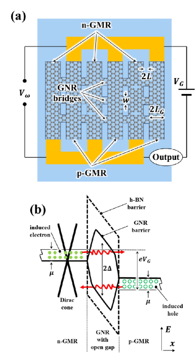
Figure 1(a) schematically shows the topological structure of the GMR-GNR array of the pairs of the interdigital GMRs. The topological properties of this device are due to two-dimensionality of graphene they could be bended if deposited on a flexible substrate.
Each GMR pair is connected by GNRs bridges, where . The GMR-GNR array is placed on the substrate, which does not degrade substantially the carrier mobility in the GMRs (for example, on the h-BN substrate). The simplest GMR-GNR detector structure may have just two GMRs (connected by one GNR).
The bias voltage between the GMR ends, , enables the formation of the 2D electron and hole gases. The bias voltage is split between the array dc resistance and the load resistance (if any, depending on the method of signal output). Thus, the coplanar GMR-GNR detector structure constitutes a lateral periodic p-GMR/n-GMR/p-GMR/…/n-GMR array. The gap opening in the GNRs leads to the formation of the energy barrier for the electron in the n-GMR and holes in the p-GMR. The operation of the GMR-GNR detector is associated with the excitation the standing plasmonic waves along the GMRs by the signal ac voltage between their ends, , induced by the impinging THz radiation collected by an antenna. These voltages result in the AC currents through the GNR bridges amplified by the rectified plasmonic resonant response. The rectified response can support the output current or output voltage signals. It is assumed that the input circuit incorporates a DC block to isolate the input and output circuits.
The GMRs have a length and a width . The GNR transverse characteristic width and the GNR length are and , respectively [see Figs. 1(a) and 1(b)]. We assume that and . The latter implies that the spacing between the GNRs is sufficiently large to prevent the carrier interaction in the neighboring GNRs and capacitive coupling between GNRs.
One of the GMR-GNR detector features is that the plasmonic wave-vectors directed along the GMRs are transverse to the inter-GMR current. The topological GMR-GNR detector structures can be, in particular, formed by the uniform graphene layer perforation. Similar devices can be based on the interdigital GMR arrays using semiconducting carbon nanotubes as bridges connecting GMRs.
Figure 1(b) shows the band diagram at the structure -cross-sections In the perforations (i.e., between the GNRs), the n- and p-GMRs are separated by relatively high energy barriers for the electrons and holes [see the dashed line in Fig. 1(b)]. The heights of these barriers are determined by the band alignment between graphene and the substrate material, for example, h-BN (although other substrate materials providing sufficiently high-quality interface and, hence, high carrier mobility in the GMRs, in particular SiC, can be used). In contrast, the GNRs provide relatively low energy barriers between the n- and p-GMRs [as shown by the solid line in Fig. 1(b)] allowing effective tunneling. These barriers are associated with the lateral confinement of the electron and hole motion (perpendicular to the GNRs) and the pertinent quantization of their energy spectra. Hence, the height of such barriers is determined by the GNR thickness and doping. As a result, the DC and AC electron and hole currents between the neighboring GMRs flow through the GNRs. We consider the arrays, in which the GNRs width is close to the characteristic value (estimated below), except, possibly, the small transition regions near the GMR-GNR contacts. The energy barrier shape in such arrays,is virtually trapezoidal turning to a triangular one at sufficiently strong bias voltage .
The linear and nonlinear components of the inter-GMR currents across the GNRs are determined by the tunneling processes. The tunneling currents are characterized by the differential conductance and the current-voltage nonlinearity parameter . Here is the inter-GNR current between the GMR edges via one GNR.
The impinging THz radiation received by an antenna induces the signal voltage , where is the THz signal voltage amplitude, is the frequency, and is the THz radiation power collected by the device antenna. The inter-GMR AC displacement current is distributed along the GMRs. It is characterized by the inter-GMR capacitance, , per unit of the GMR length.
Since all the GMR-GNR array periods are equivalent, the net signal current density (current per GMR unit length) between the neighboring GMRs (including the electron and hole currents via the GNRs and the displacement current) can be presented as
| (1) |
Here and are the signal components of the p- and n-GMRs (depending on the coordinate directed along the GMRs), respectively, is the -coordinate of the -th GNR, and is the form-factor characterizing the z-distribution of the carrier current through the GNR, which, due to the narrowness of the GNRs, is replaced by the Dirac delta function [with ].
Considering the specifics of the GMR shape (blade-like), the inter-GMR capacitance per unit length is presented as [19] with , , and , where is the dielectric constant of the substrate. We disregarded the transit delay of the electrons and holes in assuming that the GNR length is sufficiently small.
Considering the inter-GMR currents via the GNRs in the right-hand side of Eq. (1) as a small perturbation and accounting for the balance between the carriers induced in the GNRs and their output/input at the side contacts, we have the following equation for the linear components of and :
| (2) |
Here is the AC Drude longitudinal conductance of the GMRs (of the width equal to ) with being its DC value, and is the electron and hole Fermi energy and is the electron and hole collision frequency in the GMRs. The Fermi energy can be expressed via the steady-state carrier density in the GNRs : , where cm/s is the characteristic electron and hole velocity in graphene, and is the Planck constant. Accounting for that , for the Fermi energy of the carriers electrically induced carriers in the GMRs, we obtain and .
The boundary conditions given at the ends of the GMRs are:
| (3) |
III Resonant excitation of plasmonic oscillations by impinging THz radiation
Using Eqs. (2) and (3), we obtain
| (4) |
| (5) |
Here
| (6) |
where
| (7) |
are the characteristic velocity of the plasmonic wave along the GNRs and their characteristic frequency (plasmonic frequency) associated with the inter-GNR capacitance and the carrier inductance (defined as in Ref. 13), respectively, and is the frequency of the carrier scattering on impurities and acoustic phonons in the GMRs. Equations (4) and (5) yield the following spatial distribution of the ac voltage swing between the p- and n-GNRs:
| (8) |
IV Rectified signal current and voltage
Accounting for Eqs. (1) and (8), for the rectified signal current, (averaged over the period ), we arrive at
| (9) |
Assuming that the number of the GNRs , from Eqs. (8) and (9) we obtain
| (10) |
with
| (11) |
The frequency-dependent quantity is the main factor describing the plasmonic response of the GMR array.
In the circuit with the load resistance, the rectified voltage across the load resistance is presented as
| (12) |
Here is the GMR-GNR array differential resistance [see Eq. (A11)].
V Responsivity
Considering that that and the THz power are related as , where is the speed of light in vacuum and the antenna gain is set , from Eqs. (10) and (12) we arrive at the following expressions for the GMR-GNR detector current responsivity, (in the A/W units)
| (13) |
with
| (14) |
being the characteristic current responsivity of the GMR-GNR detectors under consideration. Using Eq. (14) and invoking the pertinent relations from the Appendix, we arrive at the following formula for the characteristic responsivity:
| (15) |
Here
| (16) |
and
| (17) |
are the voltage characterizing the sensitivity of the carrier density in the GMRs to the bias voltage and the tunneling voltage, respectively, and is the effective GNR width (.
As follows from Eq. (15), the characteristic current responsivity of the GMR-GNR detectors is a nonmonotonic function of the bias voltage . It reaches a maximum at , with
| (18) |
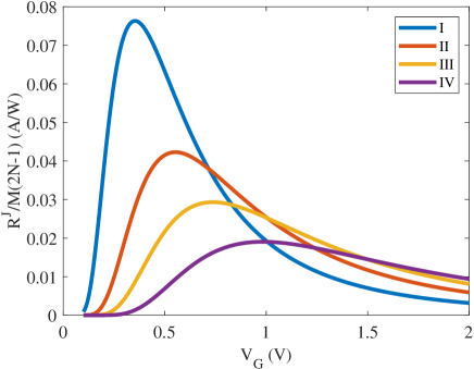
| Structure | (nm) | (nm) | (nm) | (nm) | (meV) | (mV) | (mV) | (mV) | (mV) | |
| I | 250, 375, 500 | 20 | 10 | 12.5/9.5 | 157 | 0.657 | 14 | 1238 | 354 | 165 |
| II | 250, 375, 500 | 15 | 10 | 10.0/9.5 | 196 | 0.576 | 16 | 1935 | 553 | 258 |
| III | 250, 375, 500 | 10 | 7.5 | 7.5/5/5 | 261 | 0.438 | 19 | 2580 | 737 | 344 |
| IV | 250, 375, 500 | 10 | 10 | 7.5/5.5 | 261 | 0.438 | 19 | 3440 | 983 | 457 |
Figure 2 shows the characteristic current responsivity versus bias voltage calculated using Eq. (15) for the GMR-GNR detectors with different structural parameters listed in Table I. As seen from Fig. 2, the characteristic current responsivity exhibits a pronounced maxima at a certain bias voltage. This voltage, , and the height of the responsivity maximum, max , are determined by the array structural parameters. In particular, for the parameters of structure I with , from Eq. (16) and Fig. 2 we obtain the following estimate: max A/W.
In the GMR-GNR detectors using the rectified voltage as the output, the signal dc voltage , given by Eq. (12), corresponds to the following formula for the detector voltage responsivity (in the V/W units) :
| (19) |
with
| (20) |
The factor in Eq. (20) is described by Eq. (15), but with replaced by .
If, for example, Ohm (this implies that in reality ), for the maximum values of the characteristic voltage responsivity max , corresponding to the above estimate of the current responsivity, we obtain max V/W.
For larger load resistances, in particular, compared with the GMR-GNR array dc resistance, can markedly exceed the latter values. Indeed, setting, for the definiteness, the load resistance to be equal to the array DC resistance , at the bias voltage , corresponding to the maximum of the current responsivity, and using the expressions for and [see Eqs. (A11) and (A12)], we obtain
| (21) |
For the parameters corresponding to structures I - IV, Eq. (21) yields V/W.
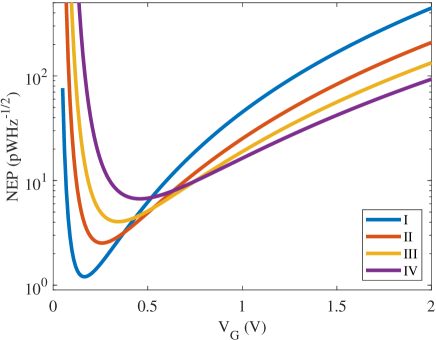
VI Noise equivalent power
To evaluate the noise equivalent power, (NEPω), of the GMR-GNR detectors receiving the THz radiation with the frequency (in the units W), we use the following formulas:
| (22) |
where is the dc current through one GNR in the absence of THz irradiation (dark current), given by Eq. (A10), and
| (23) |
is the characteristic NEP.
At the bias voltage , corresponding to the NEP minimum , from Eq. (21) we obtain
Figure 3 shows the GMR-GNR detector NEP, calculated using Eq. (23) for the GMR-GNR detectors with structures I -IV (i.e., the same structural parameters as in Fig. 2). For the definiteness, we assume that . The NEP values of GMR-GNR detectors exhibit fairly deep minima as functions of the bias voltage. The NEP minima are achieved at the bias voltage , which is about of .
VII Spectral characteristics of the GMR-GNR detectors
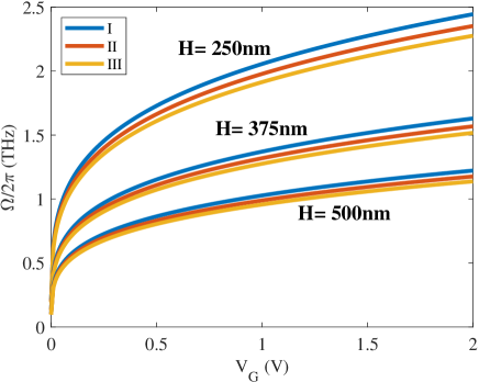
The excitation of the plasmonic oscillations (standing plasmonic waves with the wave vector directed along the GNRs) by the impinging THz radiation can result in the resonant response with the responsivities (both the current and voltage responsivities) exhibiting maxima at the plasmonic resonant frequency and its harmonics (,…). The plasmonic frequency, given by Eq. (7), is determined by the structural parameters and the bias voltage (via the dependence of on the carrier Fermi energy ).
Figure 4 shows the voltage dependence of the plasmonic frequency calculated for the structures I - IV with the different GMR lengths. The plasmonic frequency markedly increases with increasing bias voltage, although such an increase is weaker () than in the standard gated 2D heterostructure devices (where . This is common for 2D carrier systems in graphene channels (see, for example, Ref. [18]). However, a relatively small value of the capacitance in the coplanar conducting arrays in comparison with the gated structures (like FETs), is a positive factor promoting higher plasmonic frequencies.
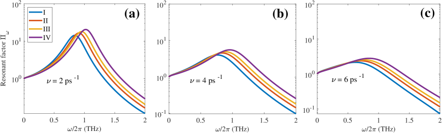
responsivity for structures I - IV for different carrier collision frequencies .
Figure 5 shows the spectral dependences of the plasmonic resonant factor for the GMR-GNR detector with structures I - IV. Calculating , we accounted for the plasmonic frequency voltage dependence shown in Fig. 4. This resonant factor is sensitive to the plasmonic oscillation quality factor , which essentially depends on the carrier scattering frequency . Since at the plasmonic resonances, , the resonant factor, as seen from Fig. 5, is large even at the room temperature corresponding to the carriers in graphene on h-BN substrate (see, for example, Refs. [23 - 31]) . For example, the carrier mobility in the GMRs, , corresponding to ps-1 and the geometrical parameter of structures I - IV at , is in the range cm2/V s. At lower temperatures or in the GMR-GNR arrays with higher plasmonic frequencies (and, hence, operating in the radiation frequencies of several THz), the resonant factor can be particularly large. Large values of the resonant factor lead to a substantial increase in the GMR-GNR detector responsivity and to the pertinent drop of their NEP.
VIII Comments
Optimal operation
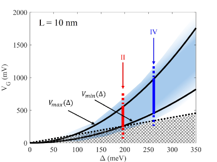
The performance of the GMR-GNR detectors under consideration depends of the structural parameters, particularly those determining the barrier height , the bias voltage , and the plasmonic resonance quality factor . The detector characteristic responsivity large at , while the characteristic NEP is small at . Hence, the voltage range can be considered as optimal for the detector operation. Since and depend on , the optimal operation can be achieved in a certain range of these quantities’ variations. Figure 6 shows such a range invoking Eq. (17): and . It is assumed, for the definiteness, that nm.
Role of the thermionic current
The inter-GMR thermionic current associated with the carriers overcoming the barrier in the GNRs was disregarded above. Since in the GMR-GNR detectors under consideration, the barrier height is virtually insensitive to the voltage drop across the GNRs (due to the trapezoidal shape of the barrier), the thermionic processes do not contribute to the ac and rectified current and, hence, do not affect the responsivity, i.e., the plots in Fig. 2.
However, the thermionic processes can lead to the following effects: First, these processes can contribute to the dark current increasing NEP. Second, the carrier heating by the impinging THz radiation can increase the thermionic current(hot-carrier bolometric mechanism of the detector operation). Both mechanisms are determined by the ratio and depend on the bias voltage .
The tunneling dark current exceeds the thermionic current (as assumed above) when , i.e., according to Eq.(A5), when . As follows from Fig. 6, the latter conditions are fulfilled for structures I - IV (with the parameters listed in Table I) in wide ranges of and . As for structure I, the thermionic dark current can be comparable with the tunneling dark current, affecting the value of NEP near its minimum. This implies that the NEP of structure I around its minimum is somewhat underestimated.
An increase in the carrier effective temperature stimulated by the THz radiation can result in the bolometric contribution to the output signal. This is similar to the THz detectors based on the gated graphene structures considered previously. [7, 13, 28, 32, 33] Our rough estimate shows that the THz detection associated with the rectification of the inter-GMR current, considered above, prevails over the hot-carrier bolometric effect if, in particular, , where is the energy relaxation time in the GMRs. The latter condition can be stricter than the above one. However, the logarithmic term is about unity even at large values of the product . The contribution of the bolometric effect in question can be beneficial for the enhancement of the GMR-GNR detectors performance being, however, characterized by a much longer response time (about of ). A more detailed consideration of the bolometric effect is beyond the scope of this work and requires a separate study.
Carrier and plasmons confinement in the GMRs.
The GMRs in the devices under consideration have a relatively small width . This can result in the band gap opening not only in GNRs but in the GMRs as well. However, the former effect is relatively weak because of ; it is accounted for by a distinction of the real and effective GMR widths, and .
The finiteness of the GMR width can lead to the quantization of the plasmon spectrum with the appearance of higher plasmonic modes. However, due to , such modes are characterized by frequencies much higher than the fundamental plasmonic frequency and the frequency of the detected THz radiation frequency .
IX Conclusion
We proposed the concept of the THz detector based on a coplanar interdigital GMR-GNR array and evaluated its performance. We showed that such detectors exhibit high values of room temperature responsivity and low noise equivalent power, which can provide their strong competitiveness with existing fast heterostructure THz detectors (see, for example, Refs. 4,7, and 36. The predicted high performance of the GMR-GNR detectors might encourage their fabrication and applications.
Acknowledgements
This work at Research Institute of Electrical Communication (RIEC), Frontier Institute for Interdisciplinary Studies (FRIIS), and University of Aizu (UoA) was supported by the Japan Society for Promotion of Science (KAKENHI grant No. 21H04546), Japan. The work at Rensselaer Polytechnic Institute (RPI) was supported by the AFOSR (contract No. FA9550-19-1-0355).
Appendix A. Electron-hole tunneling currents through GNRs
We consider the GMR-GNR arrays with the trapezoidal energy barriers for the electrons and holes in the GMRs (in the absence of the bias voltage), i.e., with a rather short transition area length. In such a case, the top of the barrier lowering is a weak function of the inter-GMR voltage. Hence, the variation of the inter-GMR current in the GNRs with varying voltage is of tunneling origin. Following the Landauer-Buttiker formula [34, 35] applied to the 1D electron and hole transport through the GNRs and accounting for the expression for the barrier transparency, the tunneling current can be presented as
| (A1) |
where at when the trapezoidal barrier transforms into to the triangular one, the tunneling transparency reads (disregarding possible short transition regions near the GMR-GNR contacts, in which the GNR width varies):
| (A2) |
is the GNR barrier tunneling transparency with
and being the electric field along the GNRs and is the barrier height for the carriers in the GNRs. The carrier energy spectra in the GNRs and the GMRs are and , where the pertinent band gap openings are estimated as and , and is the momentum along GNRs and GMRs. Hence, with .
If , , at . In this case,
| (A3) |
so that Eqs. (A1) - (A3) yield
| (A4) |
Here
| (A5) |
and
| (A6) |
is the characteristic tunneling voltage.
Equation (A4) leads to
| (A7) |
| (A8) |
so that
| (A9) |
Here
| (A10) |
is the DC current in the absence of THz irradiation (dark current per one GNR). A simplification of Eqs. (A7) - (A9) is justified when is markedly smaller than . The latter corresponds to reality. The above equations are valid if , i.e., when the barrier becomes triangular under the bias voltage.
In particular, Eq. (A10) corresponds to the GMR-GNR array differential resistance and DC resistance (which are different) equal to
| (A11) |
and
| (A12) |
respectively, therefore
| (A13) |
In particular, for structure II at we find kOhm.
References
References
- [1] M. Dyakonov and M. Shur “Detection, mixing, and frequency multiplication of terahertz radiation by two-dimensional electronic fluid,” IEEE Trans. Electron Devices 43, 380 (1996).
- [2] S. A. Maier, Plasmonics: Fundamentals and Applications (Springer, New York, 2007).
- [3] G. Barbillon “Plasmonics and its applications,” Materials 12, 1502 (2019).
- [4] A. Rogalski, “Graphene-based materials in the infrared and terahertz detector families: a tutorial,” Advances in Optics and Photonics 11, 314 (2019).
- [5] V. Ryzhii, T. Otsuji, M. S. Shur, “Graphene based plasma-wave devices for terahertz applications,” Appl. Phys. Lett. 116, 140501 (2020).
- [6] V. Ryzhii, et al., “Resonant plasmonic terahertz detection in graphene split-gate field-effect transistors with lateral p–n junctions,” J. Phys. D: Appl. Phys. 49, 315103 (2016).
- [7] D. A. Bandurin, et al., “Resonant terahertz detection using graphene plasmons,” Nat. Comm. 9, 5392 (2018).
- [8] S. Boubanga-Tombet, et al., “Room temperature amplification of terahertz radiation by grating-gate graphene structures,” Phys. Rev. X 10, 031004 (2020).
- [9] Z. Chen, A. Narita, and K. Müllen, “Graphene nanoribbons: On-surface synthesis and integration into electronic devices,” Adv. Mat. 32, 2001893 (2020).
- [10] V. Ryzhii, T. Otsuji, M. Ryzhii, V. Mitin, M. S. Shur, “Resonant plasmonic terahertz detection in gated graphene p-i-n field-effect structures enabled by nonlinearity from Zener-Klein tunneling,” Phys. Rev. Appl. 18, 0234022 (2022).
- [11] J. A. Delgado-Notario, et al., “Enhanced terahertz detection of multigate graphene nanostructures,” Nanophotonics 11, 519 (2022).
- [12] A. J. Jumaah, H. G. Roskos and S. Al-Daffaie, “Novel antenna-coupled terahertz photodetector with graphene nanoelectrodes,” APL Photon. 8, 026103 (2023).
- [13] V. Ryzhii, et al., “Resonant plasmonic detection of terahertz radiation in field-effect transistors with the graphene channel and the black-AsxP1-x gate layer,” Sci. Rep. 13, 9665 (2023).
- [14] F. Ludwig, et al., “Terahertz detection with graphene FETs: Photothermoelectric and resistive self-mixing contributions to the detector response,” ACS Appl. Electron Mater. 6, 2197 (2024).
- [15] J. M. Caridad, et al., “Room-temperature plasmon-assisted resonant THz detection in single-layer graphene transistors,” Nano Lett. 24, 935 (2024).
- [16] W. Frensley, “Frequency effects of ballistic electron transport in semiconductors,” IEEE Electron Device Lett. 61, 137 (1980).
- [17] V. Ryzhii, A. Satou, and T. Otsuji, “Plasma waves in two-dimensional electron-hole system in gated graphene heterostructures,” J. Appl. Phys. 101, 024509 (2007).
- [18] V. Ryzhii, C. Tang, T. Otsuji, M. Ryzhii, and M. S. Shur,“Terahertz plasmonic resonances in coplanar graphene nanoribbon structures,” J. Appl. Phys. 135, 114503 (2024).
- [19] V. Ryzhii, M. Ryzhii, C. Tang, T. Taiichi, M. S. Shur, “Resonant plasmonic terahertz photomixing using interdigital graphene micro-nanoribbon arrays,” Appl. Phys. Lett. 124, 163504 (2024).
- [20] A. Sh. Achoyan, A. E. Yesayan, E. M. Kazaryan, and S. G. Petrosyan, “Two-dimensional p–n junction under equilibrium conditions,” Semiconductors 36, 903 (2002).
- [21] B. Gelmont, M. Shur, and C. Moglestue, “Theory of junction between two-dimensional electron gas and p-type semiconductor,” IEEE Trans. Electron Devices 39, 1216 (1992).
- [22] O. G. Vendik, S. P. Zubko, and M. A. Nikol’skii, “Modeling and calculation of the capacitance of a planar capacitor containing a ferroelectric thin film, ” Tech. Phys. 44, 349 (1999).
- [23] T. Fang, A. Konar, H. Xing, and D. Jena, “Mobility in semiconducting graphene nanoribbons: Phonon, impurity, and edge roughness scattering, ” Phys. Rev. B 78, 205403 (2008).
- [24] K. M. Borysenko, et al., “First-principles analysis of electron-phonon interactions in graphene,” Phys. Rev. B 81, 121412R (2010).
- [25] M. Schutt, P. M. Ostrovski, I. V. Gornyi, and A. D. Mirlin, “Coulomb interaction in graphene: Relaxation rates and transport,” Phys. Rev. B 83, 155441 (2010).
- [26] M. V Fischetti, et al., “Pseudopotential-based studies of electron transport in graphene and graphene nanoribbons,” J. Phys: Cond. Mat. 25, 473202 (2013).
- [27] L. Wang, et al., “One-dimensional electrical contact to a two-dimensional material,”Science 342, 614 (203).
- [28] L. Banszerus, et al., “Ultrahigh-mobility graphene devices from chemical vapor deposition on reusable copper,” Sci. Adv. 1e1500222 (2015).
- [29] M. Yankowitz, Q. Ma, P. Jarillo-Herrero, and B. J. LeRoy, “Van der Waals heterostructures combining graphene and hexagonal boron nitride,” Nat. Rev. Phys. 1, 112 (2019).
- [30] Y. Zhang and M. S. Shur, “Collision dominated, ballistic, and viscous regimes of terahertz plasmonic detection by graphene,” J. Appl. Phys. 129, 053102 (2021).
- [31] D. Vaquero, et al., “Phonon-mediated room-temperature quantum Hall transport in graphene,”Nat. Comm. 14, 318 (2023).
- [32] V. Ryzhii, M. Ryzhii, T. Otsuji, V. Mitin, M. S. Shur, “Modulation characteristics of uncooled graphene photodetectors,” J. Appl. Phys. 129, 214503 (2019).
- [33] V. Ryzhii, et.al., “Dynamic characteristics of terahertz hot-electron graphene FET bolometers: Effect of electron cooling in channel and at side contacts,” J. Appl. Phys. 135, 194502 (2024).
- [34] M. Buttiker, Y. Imry, R. Landayer, and S. Pinhas, “Generalized many-channel conductance formula with application to small rings,” Phys. Rev. B 31, 6207 (1985).
- [35] G. Liang, N. Neophytou, D. E. Nikonov, and M. S. Lundstrom, “Performance projections for ballistic graphene nanoribbon field-effect transistors,” IEEE Trans. Electron Devices 54, 677 (2007).
- [36] U. R. Pfeiffer, J. Grzyb, H. Sherry, A. Cathelin and A. Kaiser, “Toward low-NEP room-temperature THz MOSFET direct detectors in CMOS technology,” 38th Int. Conf. on Infrared, Millimeter, and Terahertz Waves (IRMMW-THz), Mainz, Germany, pp.1-2, 2013.