Present address :]Laboratory for multifunctional ferroic materials, Department of Physics and Materials Science, University of Luxembourg, LIST-Belvaux site, 41 rue du Brill, L-4422 Belvaux, Luxembourg
Corresponding Author :] constance.toulouse@uni.lu
Giant Strain Tunability in Polycrystalline Ceramic Films via Helium Implantation
Abstract
Strain engineering is a powerful tool routinely used to control and enhance properties such as ferroelectricity, magnetic ordering, or metal-insulator transitions. Epitaxial strain in thin films allows manipulation of in-plane lattice parameters, achieving strain values generally up to 4%, and above in some specific cases. In polycrystalline films, which are more suitable for functional applications due to their lower fabrication costs, strains above 1% often cause cracking. This poses challenges for functional property tuning by strain engineering. Helium implantation has been shown to induce negative pressure through interstitial implantation, which increases the unit cell volume and allows for continuous strain tuning with the implanted dose in epitaxial monocrystalline films. However, there have been no studies on the transferability of helium implantation as a strain-engineering technique to polycrystalline films. Here, we demonstrate the technique’s applicability for strain engineering beyond epitaxial monocrystalline samples. Helium implantation can trigger an unprecedented lattice parameter expansion up to 3.2% in polycrystalline BiFeO3 films without causing structural cracks. The film maintains stable ferroelectric properties with doses up to . This finding underscores the potential of helium implantation in strain engineering polycrystalline materials, enabling cost-effective and versatile applications.
I Introduction
Tuning and controlling functional properties is a key challenge for materials sciences and its applications. A powerful way to control, enhance, or even induce functional properties that is now routinely implemented, is the use of strain-engineering. It allows the tuning of ferroelectric propertiesChoi et al. (2004); Infante et al. (2010); Xu et al. (2020), magnetic ordersSando et al. (2013); Agbelele et al. (2016), metal-insulator transitionsWang et al. (2019) and electro-optical propertiesBlázquez Martínez et al. (2023); Paillard, Prokhorenko, and Bellaiche (2019); Fredrickson et al. (2018) among others.
In thin films, manipulating epitaxial strain is a well-known strategy to control the in-plane lattice parameters while the out-of-plane lattice parameters are imposed by the strain accommodation. The typical range of accessible in-plane strain yielded by epitaxy usually lies within 3-4% of lattice mismatchSando (2022). In epitaxial BiFeO3 films, values of in-plane compressive strain larger than 4% have been achieved by choosing the appropriate lattice mismatch between the film and the substrate to favor the transition towards the supertetragonal polymorphZeches et al. (2009). In polycrystalline films, which are more suited for functional applications due to their lower fabrication costsMuralt (2000) and compatibility with low-temperature processing techniquesSong et al. (2024), the in-plane strain can also be controlled by the choice of substrate. This is typically achieved by either choosing substrates with a different thermal expansion coefficient Won et al. (2019), or by deposition on flexible substratesYang et al. (2019). Reported strain values remain typically below 1%Brennecka et al. (2004); Martínez et al. (2023); Moreira et al. (2024); Defay and Glinsek (2021). Since polycrystalline films are more brittle than their epitaxial counterparts, strain values larger than 0.5% in perovskite compounds result in structural cracking,Coleman et al. (2019) making it challenging to engineer their functional properties through strain.
Negative pressure, to be understood as an increase of the volume of the material’s unit cellImre (2007), has been theoretically shown to be a very promising strategy to tune functional properties in materialsLiu et al. (2009); Tinte, Rabe, and Vanderbilt (2003); Aligia et al. (2001); Sharma et al. (2017). However, due to the technically challenging nature of achieving negative pressure, it has been experimentally under-explored. Chemical doping with substitution by species with higher ionic radius results in an increase in volume. Nevertheless, this modifies the chemical composition of the material and results in effects that are not purely due to the induced deformationBarazani et al. (2023). Tensile in-plane strain, resulting from depositing thin films on substrates with higher lattice parameters, can also be seen as bi-axial negative strainAguirre-Tostado et al. (2004). However, it can only induce discrete states of negative pressure, which depend on the chosen substrates and does not correspond to a continuously tunable parameter.
Previous studies have demonstrated that implanted helium can be used to introduce uniaxial out-of-plane negative pressure.Guo et al. (2015); Toulouse et al. (2021) Being a noble gas, helium does not form bonds and implants interstitially, causing the material to expand. This volume increase can be tuned continuously with the implanted helium dose, up to the limit of amorphization. The amorphization threshold is found to be around He.cm-2 for oxide perovskitesLivengood et al. (2009).
BiFeO3 is an extensively studied multiferroic materialHeron et al. (2011): it becomes ferroelectric below K in the bulkLebeugle et al. (2007a), and exhibits a G-type antiferromagnetic ordering of the Fe spins with a superimposed cycloidal modulation at temperatures below K Lebeugle et al. (2007b). In thin films, due to symmetry lowering, the usual rhombohedral structure of the bulk phase at ambient conditions becomes monoclinic, in a phase called R-like because of its similarity with the bulk rhombohedral phase. Under high compressive epitaxial strain, the BiFeO3 thin films transition towards the so-called supertetragonal polymorph or T-like phaseSando et al. (2016) which is also in a monoclinic space group due to the symmetry lowering of the film geometry, and for which the ratio between the c and a lattice parameters reaches 1.23.
Under helium implantation, BiFeO3 films transition towards this supertetragonal phase under lower epitaxial strain than virgin non-implanted filmsHerklotz et al. (2019a); Toulouse et al. (2021); Chen et al. (2019). The nature of the transition (first or second order) is still debated, but an intermediate mixed phase with a coexistence of the R-like and the T-like phases is consistently observed. So far, only structural and no functional properties of BiFeO3films have been studied under negative pressure by helium implantation, except for a recent study showing the formation of antiphase domain walls in He-implanted BiFeO3 filmsCai et al. (2023).
So far, all previous studies using helium implantation for strain engineering have been performed in epitaxial monocrystalline films. Until now, there have been no studies on the use of helium implantation for strain-engineering of polycrystalline films. Here, we demonstrate that we can induce a tunable uniaxial strain of up to 3.2%. Remarkably, the ferroelectric properties of the ceramic remain stable at these high strain levels, underscoring the exceptional capability of helium implantation to achieve tunable strain in polycrystalline materials. This high strain value, coupled with the preservation of the microstructure and functional properties, is unprecedented in polycrystalline films; prior strategies only achieved strain tunability below 1%, with cracks typically developing at strain levels higher than 0.5%.Coleman et al. (2019); Brennecka et al. (2004); Martínez et al. (2023); Moreira et al. (2024)
II Materials and methods
II.1 Thin films synthesis
Polycrystalline and structurally textured BiFeO3 films were grown by chemical solution deposition as described in a previous workBlázquez-Martínez et al. (2021). Films with different pristine strain states were studied. To do so, the films were deposited on substrates with different thermal expansion coefficients: MgO (Biotain Crystal, China), c-cut sapphire (Sap), and fused silica (FS) substrates (both Siegert Wafer, Germany). Before the deposition, the substrates were coated with of non-ferroelectric atomic-layer-deposited \chHfO2 film to prevent diffusion during film fabrication, and a 13 nm-thick \chPbTiO3 seed layer to obtain -textured films. The thickness of all the BiFeO3 films was set to . Both pure BiFeO3(BFO) and BiFeO3 co-doped with 5% manganese and 2% titanium substituting on the Fe sites (BFMTO), more suited for electrical measurements due to their lower electrical leakage Qi et al. (2005); Singh et al. (2007); Kawae et al. (2009); Raghavan, Kim, and Kim (2014); Blázquez-Martínez et al. (2021), were studied in this work.
Four samples were used for the structural characterization, one pure BiFeO3film on fused silica (BFO/FS) as a reference and 5% manganese and 2% titanium co-doped BiFeO3 films (BFMTO) on three different substrates: BFMTO/FS, BFMTO/Sap and BFMTO/MgO with different in-plane strain states reported previously as -0.22% on MgO, +0.1% on sapphire, and +0.38% on fused silicaMartìnez et al. (2023).
Interdigitated electrodes (IDEs) were used on BFMTO/Sap to measure the electrical properties in-planeBlázquez Martínez et al. (2022); Aruchamy et al. (2022): conventional lift-off photolithography and platinum sputtering were used to pattern the IDEs on top of the films. The IDEs were encapsulated using an epoxy-based photoresist (SU-8 3000, Kayacu Advanced Materials, USA) to prevent electric arcing between the fingers during the high voltage switching. To probe the out-of-plane electrical properties, we used a metal-insulator-metal geometry (MIM) in BFMTO/PtSi, where circular In:SnO2 and Pt top electrodes with diameter and thickness were patterned by lift-off photolithography and deposited by sputtering.
II.2 Helium implantation
The local implantation of helium was done using an Orion NanoFab Helium Ion Microscope (HIM) from Zeiss, which allows for a resolution for patterning down to the nanoscaleZeiss (2008). For samples destined for synchrotron micro-XRD analysis, the patterning of the implanted regions was set to square regions of 450450µm2 size to allow for analysis with the X-ray beam fully inside of the implanted region. For the samples destined for electrical measurements, we implanted regions corresponding to the surface needed for electrode deposition, namely 350750µm2 for the IDEs, and 200200µm2 for the MIM configuration.
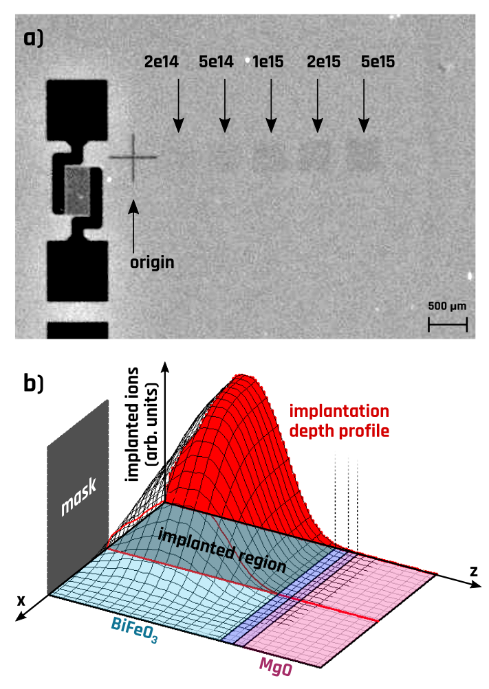
Figure 1.a shows an optical microscopy image of the BFO/MgO film after implantation. The different implanted regions are visible with a variable contrast. This change in the optical properties is likely due to surface pollutionHerklotz et al. (2019b), although the strong elasto-optic coupling in BiFeO3 could also play a role in this optical changeSando et al. (2014). In any case, this change of contrast as well as the observed structural changes are still present twelve months after implantation.
The adequate implantation parameters, namely energy - that controls the implantation depth profile, shown in red on Figure 1.b - and the implanted dose - that controls the strain -, were determined using Monte Carlo simulations performed using the Stopping Range of Ions in Matter (SRIM) software packageZiegler (2004). The energy was set to , such that the maximum of the implantation depth profile is located in the center of the BiFeO3 layer. The different samples were implanted with doses ranging from to , chosen to be below the amorphization threshold for BiFeO3Toulouse et al. (2021). The simulations were done with a mask to reproduce the implantation obtained with the scanning mode of the helium microscope and the in-plane dose gradient at the interface is visible along the x-axis. The size of the in-plane dose gradient, corresponding to the width of the interface between the implanted and non-implanted regions is around .
II.3 Structural and electrical characterization
Micro-XRD measurements were performed on the CRISTAL beamline at the SOLEIL synchrotron source during two successive beamtimes. The wavelength of the beam was of and , corresponding to an energy of and respectively.
Two different configurations were used to observe the effects of helium implantation: a reflection geometry, with the wavevector near the normal of the film, to characterize the out-of-plane structure, and a transmission geometry where the wavevector transfer lies very close to the plane of the film. Due to the presence of some of the substrate’s Bragg peaks close to the peaks of the layers we were observing (for instance the ), we measured with a slight misalignment of 3 that results in a change of relative intensity between different Bragg peaks.
Polarization hysteresis loops were measured on a Thin Film Analyzer TF 2000 (aixACCT, Germany) at room temperature and at a frequency of . DC current density-electric field measurements were performed on unpoled films with a step of and a duration of per step.
III Results and discussion
III.1 Structural characterization
Details about the microstructure and strain analysis of the different films are identical to those reported previouslyMartìnez et al. (2023). All films show a granular microstructure with a grain diameter around . The pristine in-plane residual thermal strain of the films grown on fused silica, sapphire, and MgO (0.38%, 0.10%, and -0.22% respectively), result from the different thermal expansion coefficients.
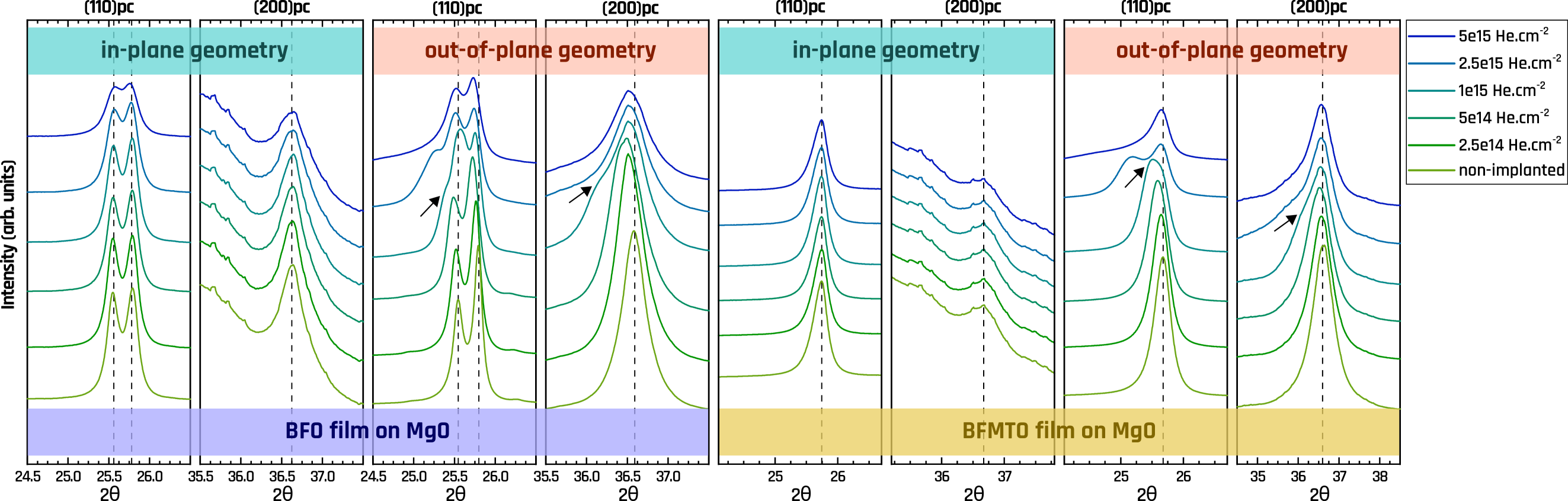
To determine the effect of helium implantation on the structure of the BiFeO3 films, micro-XRD measurements were performed on the different helium implanted regions on each sample. Figure 2 exemplarily shows the scans of the and peak under different Helium doses for BFO/MgO and BFMTO/MgO.
A shift towards lower angles, i.e., larger lattice parameter, with increasing implanted helium dose is observed. Under higher doses, the appearance of a new peak reveals the presence of a strained phase at lower angles with the subsistence of the non-strained phase at the original resulting in phase-mixing, as expected for the structural transition towards the supertetragonal polymorph observed in epitaxial films under implantationHerklotz et al. (2019a); Toulouse et al. (2021). The scans for the different films with different doses are shown in the supplementary information.
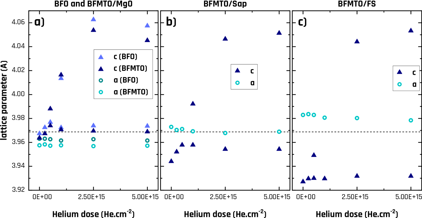
For each film, the in-plane (a) and out-of-plane (c) lattice parameters were extracted from the Bragg peak measured in reflection and transmission geometries. Figure 3 shows the lattice parameter evolution for different helium doses in films with different pristine strain states. The pristine strain state was evaluated in the non-implanted regions. Different ratios were measured in the different films as expected from the different thermal expansion coefficients of the substrates. The lattice parameter ratios are 1.003, 0.992 and 0.985 for BFMTO/MgO, BFMTO/Sap and BFMTO/FS, respectively. This is consistent with previously measured pristine strain statesMartìnez et al. (2023).
An out-of-plane expansion of the unit cell without any change in the plane is observed in all the samples with increasing helium dose. Slightly lower c-axis expansion with respect to the pristine state is observed in BFMTO compared to the BFO films. In all samples, the implantation-driven strain saturates around dose. Above that, at the dose, the strain-induced peaks observed in the XRD scans broaden and their intensity considerably decreases, which we attribute to a significant lowering of crystallinity due to implantation at a higher dose.
A clear influence of the pristine strain state is observed. Higher pristine in-plane strain results in higher out-of-plane lattice parameter increase with helium implantation. The measured c-axis expansion with saturation-level implantation is of 2.26% on BFMTO/MgO (for 0.22% compressive in-plane strain), 2.72% on BFMTO/Sap (for 0.1% tensile in-plane strain) and 3.21% on BFMTO/FS (for 0.38% tensile in-plane strain).
III.2 Electrical properties
The influence of He-implantation on the electrical properties was studied in two geometries: out-of-plane, using MIM capacitors of BFMTO on platinized silicon and in-plane, using IDE capacitors on BFMTO/Sap.
The curves of the Pt/BFMTO/Pt MIM capacitor as a function of the implanted He dose are displayed in Figure 4.c. Stable ferroelectric switching is observed in all samples with doses up to . A small decrease of the remnant polarization Pr is observed with increasing helium dose. At doses higher than , the ferroelectric domain structure does not switch anymore (Fig.4.c inset, dotted lines). This could be due to the progressive increase of the coercive electric field under helium (visible with the maxima of the curves on the inset of Fig 4.c). The supertetragonal polymorph of BiFeO3is known to have a higher ferroelectric switching field Sando et al. (2016); Xu et al. (2017). In this scope, the increase in tetragonality under helium implantation seen in XRD is consistent with an increase in the out-of-plane switching field. A loss in crystallinity, reflected in the XRD peak width, would lead to the same effect.
The in-plane switching characteristic using IDE geometry is shown in Figure 4.d. A decrease in the remnant polarization Pr is also observed with increasing helium dose. At the highest dose, the implantation also nearly suppresses the ferroelectric switching behavior. However, unlike what is observed in the MIM geometry, the coercive switching field does not shift appreciably (inset Fig. 4.d).
DC current density measurements under electric field (-) were performed. To avoid contributions from displacement currents due to polarization switching, the curves were only measured at electric fields below 30% of the coercive field. The - curves for both configurations are displayed in Figure 4.e and 4 .f. A reduction of the leakage current density is observed with helium implantation.
III.3 Discussion
Helium implantation allows for a continuously tunable increase of the out-of-plane lattice parameter in all the films. This indicates the transferability of the technique to strain engineer polycrystalline films, with a narrower strain range compared to their epitaxial counterpartsGuo et al. (2018); Toulouse et al. (2021). Despite a more complex microstructure and the presence of randomly oriented domains and grain boundaries, helium implantation still induces an out-of-plane strain with a lower out-of-plane lattice parameter expansion compared to epitaxial films. For epitaxial samples, an out-of-plane lattice parameter tunability up to 9% has been reported in BiFeO3 films deposited on \chSrTiO3Toulouse et al. (2021). In polycrystalline samples, the tunability only reaches a maximum value of 3.2% in BiFeO3/FS. However, these values are one order of magnitude larger than what can be achieved using substrates with thermal expansion coefficient strongly dissimilar from that of the film, showing the potential of helium implantation as a strain engineering technique in polycrystalline samples. Contrary to what is observed in compressively strained epitaxial films, the onset of the transition towards the supertetragonal phase is not yet reached for the values of strain and ratio achieved here: up to 1.03 for the BFO/MgO film, well below the 1.23 of the T-phase. Our polycrystalline films stay in an R-like phase, with an out-of-plane elongation tunable under helium dose.
The pristine strain state plays a key role in the lattice parameter expansion upon helium implantation: the higher in-plane strain results in higher out-of-plane lattice parameter expansion. Additionally, the peak splitting in the x-ray diffractograms at higher doses indicates the coexistence of strained and non-strained regions in the film. In agreement with the SRIM simulations (Fig. 1.b), a skewed normal distribution of helium concentration is expected, resulting in a strain gradient within the film thickness that could explain this coexistence.
Stable ferroelectric switching is observed with helium doses up to . The absence of any strong change in the Pr values is in agreement with the structure of the film remaining in a strained rhombohedral phase with no change in texture. In this phase, only subtle changes in the Pr are expected Sando et al. (2016) and observed in this work, which supports the idea that helium affects strain only and does not lead to any significant modification of the dielectric - and here ferroelectric - properties in the material. Additionally, a decrease of conductivity in the BiFeO3 with increasing helium implantation is observed. This may not be a strain-induced effect, but could rather be attributed to the formation of defect complexes with increasing helium dose as previously shown in helium implanted epitaxial \chPbTiO3 filmsSaremi et al. (2016, 2018a), or epitaxial BiFeO3Saremi et al. (2018b) and epitaxial PMN-PT filmsKim et al. (2020).
IV Conclusion and outlook
We studied the influence of helium implantation on the structural and electrical properties of textured polycrystalline BiFeO3 under different pristine strain states. An increase of the lattice parameter up to 3.2% and 2.3% in BiFeO3 films under compressive and tensile strain respectively, was measured.
These results demonstrate a method to induce unprecedented large out-of-plane strain values in polycrystalline films, highlighting that grain boundaries do not prevent the interstitial implantation of helium atoms in the grains. The skewed normal distribution of helium concentration in the film induces differently strained areas through the thickness of the film, which results in the coexistence of strained and non-strained R-like regions. Because helium ion implantation can produce these high strain values in application-compatible polycrystalline thin films, it holds promise as a strategy to tune the strain-dependent properties of polycrystalline ceramics such as piezoelectricity or electro-optic coefficients. Additionally, the possibility to tune the helium concentration profile by modifying the implantation parameters such as energy or incident angle opens the path to inducing additional flexo-electric functionalities to polycrystalline materials.
Author contributions
The samples were synthesized and electrodes were deposited by A.B.M. and S.G. SRIM simulations and determination of implantation parameters were done by C.T. Helium implantation was performed by J-N.A. and C.T. Electrical measurements were performed by A.B.M., T.G. and C.T. The synchrotron experiments on the CRISTAL beamline were done by A.B.M., M.G. and C.T. as users and P.F. as a beamline scientist and local contact. C.T. was the main proposer for both synchrotron proposals and performed the XRD data analysis. The paper was written by C.T., A.B.M and M.G, and was read and commented upon by all co-authors. C.T. coordinated the study.
Acknowledgments
Supported by the Luxembourg National Research Fund (FNR) (FNR/C21/MS/16335086/Toulouse). A.B.M., S.G., and T.G. also acknowledge support by the Luxembourg National Research Fund (FNR) (PRIDE17/12246511/PACE).
We acknowledge the SOLEIL Synchrotron facility for the provision of synchrotron radiation at the CRISTAL beamline (proposals number 20210545 and 20221603).
This research was funded in whole, or in part, by the Luxembourg National Research Fund (FNR), grant reference FNR/C21/MS/16335086/Toulouse. For the purpose of open access, and in fulfilment of the obligations arising from the grant agreement, the author has applied a Creative Commons Attribution 4.0 International (CC BY 4.0) license to any Author Accepted Manuscript version arising from this submission.
The authors have no conflicts to disclose.
The data that support the finding of this study are available from the corresponding author upon reasonable request.
References
- Choi et al. (2004) K. J. Choi, M. Biegalski, Y. L. Li, A. Sharan, J. Schubert, R. Uecker, P. Reiche, Y. B. Chen, X. Q. Pan, V. Gopalan, L.-Q. Chen, D. G. Schlom, and C. B. Eom, “Enhancement of ferroelectricity in strained BaTiO3 thin films,” Science 306, 1005–1009 (2004).
- Infante et al. (2010) I. C. Infante, S. Lisenkov, B. Dupé, M. Bibes, S. Fusil, E. Jacquet, G. Geneste, S. Petit, A. Courtial, J. Juraszek, L. Bellaiche, A. Barthélémy, and B. Dkhil, “Bridging Multiferroic Phase Transitions by Epitaxial Strain in BiFeO3,” Physical Review Letters 105 (2010), 10.1103/PhysRevLett.105.057601.
- Xu et al. (2020) R. Xu, J. Huang, E. S. Barnard, S. S. Hong, P. Singh, E. K. Wong, T. Jansen, V. Harbola, J. Xiao, B. Y. Wang, S. Crossley, D. Lu, S. Liu, and H. Y. Hwang, “Strain-induced room-temperature ferroelectricity in SrTiO3 membranes,” Nature Communications 11, 3141 (2020).
- Sando et al. (2013) D. Sando, A. Agbelele, D. Rahmedov, J. Liu, P. Rovillain, C. Toulouse, I. C. Infante, A. P. Pyatakov, S. Fusil, E. Jacquet, C. Carrétéro, C. Deranlot, S. Lisenkov, D. Wang, J.-M. Le Breton, M. Cazayous, A. Sacuto, J. Juraszek, A. K. Zvezdin, L. Bellaiche, B. Dkhil, A. Barthélémy, and M. Bibes, “Crafting the magnonic and spintronic response of bifeo3 films by epitaxial strain,” Nature Materials 12, 641–646 (2013).
- Agbelele et al. (2016) A. Agbelele, D. Sando, C. Toulouse, C. Paillard, R. D. Johnson, R. Rüffer, A. F. Popkov, C. Carrétéro, P. Rovillain, J.-M. Le Breton, B. Dkhil, M. Cazayous, Y. Gallais, M.-A. Méasson, A. Sacuto, P. Manuel, A. K. Zvezdin, A. Barthélémy, J. Juraszek, and M. Bibes, “Strain and Magnetic Field Induced Spin-Structure Transitions in Multiferroic BiFeO3,” Advanced Materials 29, 1602327 (2016).
- Wang et al. (2019) C. Wang, H. Zhang, K. Deepak, C. Chen, A. Fouchet, J. Duan, D. Hilliard, U. Kentsch, D. Chen, M. Zeng, X. Gao, Y.-J. Zeng, M. Helm, W. Prellier, and S. Zhou, “Tuning the metal-insulator transition in epitaxial SrVO3 films by uniaxial strain,” Physical Review Materials 3, 115001 (2019).
- Blázquez Martínez et al. (2023) A. Blázquez Martínez, P. Grysan, S. Girod, S. Glinšek, N. Aruchamy, P. Biswas, M. Guennou, and T. Granzow, “Strain engineering of the electro-optic effect in polycrystalline BiFeO3 films,” Optical Materials Express 13, 2061 (2023).
- Paillard, Prokhorenko, and Bellaiche (2019) C. Paillard, S. Prokhorenko, and L. Bellaiche, “Strain engineering of electro-optic constants in ferroelectric materials,” npj Computational Materials 5, 6 (2019).
- Fredrickson et al. (2018) K. D. Fredrickson, V. V. Vogler-Neuling, K. J. Kormondy, D. Caimi, F. Eltes, M. Sousa, J. Fompeyrine, S. Abel, and A. A. Demkov, “Strain enhancement of the electro-optical response in BaTiO3 films integrated on Si(001),” Physical Review B 98, 075136 (2018).
- Sando (2022) D. Sando, “Strain and orientation engineering in ABO3 perovskite oxide thin films,” Journal of Physics: Condensed Matter 34, 153001 (2022).
- Zeches et al. (2009) R. J. Zeches, M. D. Rossell, J. X. Zhang, A. J. Hatt, Q. He, C.-H. Yang, A. Kumar, C. H. Wang, A. Melville, C. Adamo, G. Sheng, Y.-H. Chu, J. F. Ihlefeld, R. Erni, C. Ederer, V. Gopalan, L. Q. Chen, D. G. Schlom, N. A. Spaldin, L. W. Martin, and R. Ramesh, “A strain-driven morphotropic phase boundary in BiFeO3,” Science 326, 977–980 (2009).
- Muralt (2000) P. Muralt, “Ferroelectric thin films for micro-sensors and actuators: a review,” Journal of Micromechanics and Microengineering 10, 136–146 (2000).
- Song et al. (2024) L. Song, J. Cardoletti, A. B. Martínez, A. Benčan, B. Kmet, S. Girod, E. Defay, and S. Glinšek, “Crystallization of piezoceramic films on glass via flash lamp annealing,” Nature Communications 15, 1890 (2024).
- Won et al. (2019) S. S. Won, H. Seo, M. Kawahara, S. Glinšek, J. Lee, Y. Kim, C. K. Jeong, A. I. Kingon, and S.-H. Kim, “Flexible vibrational energy harvesting devices using strain-engineered perovskite piezoelectric thin films,” Nano Energy 55, 182–192 (2019).
- Yang et al. (2019) C. Yang, Y. Han, J. Qian, P. Lv, X. Lin, S. Huang, and Z. Cheng, “Flexible, temperature-resistant, and fatigue-free ferroelectric memory based on Bi(Fe0.93Mn0.05Ti0.02)O3 thin film,” ACS Applied Materials & Interfaces 11, 12647–12655 (2019), https://doi.org/10.1021/acsami.9b01464 .
- Brennecka et al. (2004) G. L. Brennecka, W. Huebner, B. A. Tuttle, and P. G. Clem, “Use of stress to produce highly oriented tetragonal lead zirconate titanate (pzt 40/60) thin films and resulting electrical properties,” Journal of the American Ceramic Society 87, 1459–1465 (2004), https://ceramics.onlinelibrary.wiley.com/doi/pdf/10.1111/j.1551-2916.2004.01459.x .
- Martínez et al. (2023) A. B. Martínez, P. Grysan, S. Girod, V. Kovacova, S. Glinšek, and T. Granzow, “Stress-tuning the bulk photovoltaic response in polycrystalline bismuth ferrite films,” Applied Physics Letters 122, 152903 (2023).
- Moreira et al. (2024) M. Moreira, J. Crêpellière, J. Polesel-Maris, R. Leturcq, J. Guillot, Y. Fleming, and P. Lunca-Popa, “Electrical properties of strained off-stoichiometric Cu–Cr–O delafossite thin films,” Journal of Physics Condensed Matter 36 (2024), 10.1088/1361-648X/ad2a07.
- Defay and Glinsek (2021) T. S. A. B. G. D. O. C. N. V. B. E. A. N. A. T. G. E. Defay and S. Glinsek, “Enhancement of ferroelectricity and orientation in solution-derived hafnia thin films through heterogeneous grain nucleation,” Applied Physics Letters , 162902 (2021), aIP Publishing.
- Coleman et al. (2019) K. Coleman, J. Walker, T. Beechem, and S. Trolier-Mckinstry, “Effect of stresses on the dielectric and piezoelectric properties of Pb(Zr0.52Ti0.48)O3 thin films,” Journal of Applied Physics 126 (2019), 10.1063/1.5095765.
- Imre (2007) A. R. Imre, “On the existence of negative pressure states,” physica status solidi (b) 244, 893–899 (2007).
- Liu et al. (2009) Y. Liu, L. Ni, Z. Ren, G. Xu, C. Song, and G. Han, “Negative pressure induced ferroelectric phase transition in rutile TiO2,” Journal of Physics: Condensed Matter 21, 275901 (2009).
- Tinte, Rabe, and Vanderbilt (2003) S. Tinte, K. M. Rabe, and D. Vanderbilt, “Anomalous enhancement of tetragonality in PbTiO3 induced by negative pressure,” Physical Review B 68, 144105 (2003).
- Aligia et al. (2001) A. A. Aligia, P. Petrone, J. O. Sofo, and B. Alascio, “Metal-insulator transition in the double perovskites,” Physical Review B 64, 092414 (2001).
- Sharma et al. (2017) V. Sharma, A. Herklotz, T. Z. Ward, and F. A. Reboredo, “Designing functionality in perovskite thin films using ion implantation techniques: Assessment and insights from first-principles calculations,” Scientific Reports 7, 1–10 (2017), number: 1 Publisher: Nature Publishing Group.
- Barazani et al. (2023) E. Barazani, D. Das, C. Huang, A. Rakshit, C. Saguy, P. Salev, J. del Valle, M. C. Toroker, I. K. Schuller, and Y. Kalcheim, “Positive and negative pressure regimes in anisotropically strained V2O3 films,” Advanced Functional Materials 33 (2023), 10.1002/adfm.202211801.
- Aguirre-Tostado et al. (2004) F. S. Aguirre-Tostado, A. Herrera-Gómez, J. C. Woicik, R. Droopad, Z. Yu, D. G. Schlom, J. Karapetrova, P. Zschack, and P. Pianetta, “Displacive phase transition in SrTiO3 thin films grown on Si(001),” Journal of Vacuum Science & Technology A: Vacuum, Surfaces, and Films 22, 1356–1360 (2004).
- Guo et al. (2015) H. Guo, S. Dong, P. D. Rack, J. D. Budai, C. Beekman, Z. Gai, W. Siemons, C. M. Gonzalez, R. Timilsina, A. T. Wong, A. Herklotz, P. C. Snijders, E. Dagotto, and T. Z. Ward, “Strain Doping: Reversible Single-Axis Control of a Complex Oxide Lattice via Helium Implantation,” Physical Review Letters 114, 256801 (2015).
- Toulouse et al. (2021) C. Toulouse, J. Fischer, S. Farokhipoor, L. Yedra, F. Carlà, A. Jarnac, E. Elkaim, P. Fertey, J.-N. Audinot, T. Wirtz, B. Noheda, V. Garcia, S. Fusil, I. P. Alonso, M. Guennou, and J. Kreisel, “Patterning enhanced tetragonality in BiFeO3 thin films with effective negative pressure by helium implantation,” Physical Review Materials 5, 024404 (2021), publisher: American Physical Society.
- Livengood et al. (2009) R. Livengood, S. Tan, Y. Greenzweig, J. Notte, and S. McVey, “Subsurface damage from helium ions as a function of dose, beam energy, and dose rate,” Journal of Vacuum Science & Technology: Part B-Microelectronics & Nanometer Structures 27, 3244–3249 (2009).
- Heron et al. (2011) J. T. Heron, M. Trassin, K. Ashraf, M. Gajek, Q. He, S. Y. Yang, D. E. Nikonov, Y.-H. Chu, S. Salahuddin, and R. Ramesh, “Electric-field-induced magnetization reversal in a ferromagnet-multiferroic heterostructure,” Physical Review Letters 107, 217202 (2011).
- Lebeugle et al. (2007a) D. Lebeugle, D. Colson, A. Forget, and M. Viret, “Very large spontaneous electric polarization in BiFeO3 single crystals at room temperature and its evolution under cycling fields,” Applied Physics Letters 91, 022907 (2007a), publisher: American Institute of Physics.
- Lebeugle et al. (2007b) D. Lebeugle, D. Colson, A. Forget, M. Viret, P. Bonville, J. F. Marucco, and S. Fusil, “Room-temperature coexistence of large electric polarization and magnetic order in BiFeO3 single crystals,” Physical Review B 76, 024116 (2007b).
- Sando et al. (2016) D. Sando, B. Xu, L. Bellaiche, and V. Nagarajan, “A multiferroic on the brink: Uncovering the nuances of strain-induced transitions in BiFeO3,” Applied Physics Reviews 3, 011106 (2016).
- Herklotz et al. (2019a) A. Herklotz, S. F. Rus, N. Balke, C. Rouleau, E.-J. Guo, A. Huon, S. KC, R. Roth, X. Yang, C. Vaswani, J. Wang, P. P. Orth, M. S. Scheurer, and T. Z. Ward, “Designing Morphotropic Phase Composition in BiFeO3,” Nano Letters (2019a), 10.1021/acs.nanolett.8b04322.
- Chen et al. (2019) C. Chen, C. Wang, X. Cai, C. Xu, C. Li, J. Zhou, Z. Luo, Z. Fan, M. Qin, M. Zeng, X. Lu, X. Gao, U. Kentsch, P. Yang, G. Zhou, N. Wang, Y. Zhu, S. Zhou, D. Chen, and J.-M. Liu, “Controllable defect driven symmetry change and domain structure evolution in BiFeO3 with enhanced tetragonality,” Nanoscale 11, 8110–8118 (2019).
- Cai et al. (2023) X. Cai, C. Chen, L. Xie, C. Wang, Z. Gui, Y. Gao, U. Kentsch, G. Zhou, X. Gao, Y. Chen, S. Zhou, W. Gao, J.-M. Liu, Y. Zhu, and D. Chen, “In-plane charged antiphase boundary and 180° domain wall in a ferroelectric film,” Nature Communications 14, 8174 (2023).
- Blázquez-Martínez et al. (2021) A. Blázquez-Martínez, N. Godard, N. Aruchamy, C. Milesi-Brault, O. Condurache, A. Bencan, S. Glinšek, and T. Granzow, “Solution-processed \chBiFeO3 thin films with low leakage current,” Journal of the European Ceramic Society 41, 6449–6455 (2021).
- Qi et al. (2005) X. Qi, J. Dho, R. Tomov, M. G. Blamire, and J. L. MacManus-Driscoll, “Greatly reduced leakage current and conduction mechanism in aliovalent-ion-doped \chBiFeO3,” Applied Physics Letters 86, 062903 (2005).
- Singh et al. (2007) S. K. Singh, H. Ishiwara, K. Sato, and K. Maruyama, “Microstructure and frequency dependent electrical properties of Mn-substituted \chBiFeO3 thin films,” Journal of Applied Physics 102, 094109 (2007).
- Kawae et al. (2009) T. Kawae, Y. Terauchi, H. Tsuda, M. Kumeda, and A. Morimoto, “Improved leakage and ferroelectric properties of Mn and Ti codoped \chBiFeO3 thin films,” Applied Physics Letters 94, 112904 (2009).
- Raghavan, Kim, and Kim (2014) C. M. Raghavan, J. W. Kim, and S. S. Kim, “Effects of Ho and Ti doping on structural and electrical properties of \chBiFeO3 thin films,” Journal of the American Ceramic Society 97, 235–240 (2014).
- Martìnez et al. (2023) A. B. Martìnez, P. Grysan, S. Girod, V. Kovacova, S. Glinšek, and T. Granzow, “Stress-tuning the bulk photovoltaic response in polycrystalline bismuth ferrite films,” Applied Physics Letters 122 (2023), 10.1063/5.0136800.
- Blázquez Martínez et al. (2022) A. Blázquez Martínez, P. Grysan, S. Girod, S. Glinšek, and T. Granzow, “Direct evidence for bulk photovoltaic charge transport in a ferroelectric polycrystalline film,” Scripta Materialia 211, 114498 (2022).
- Aruchamy et al. (2022) N. Aruchamy, T. Schenk, S. Girod, S. Glinšek, E. Defay, and T. Granzow, “Influence of substrate stress on in-plane and out-of-plane ferroelectric properties of PZT films,” Journal of Applied Physics 131 (2022), 10.1063/5.0072503.
- Zeiss (2008) C. Zeiss, “Microscopy resolution record claimed by Carl Zeiss, (http://www.fabtech.org/news),” Tech. Rep. (Zeiss, Carl, 2008).
- Herklotz et al. (2019b) A. Herklotz, S. F. Rus, C. Sohn, S. KC, V. R. Cooper, E.-J. Guo, and T. Z. Ward, “Optical response of BiFeO3 films subjected to uniaxial strain,” Physical Review Materials 3, 094410 (2019b), publisher: American Physical Society.
- Sando et al. (2014) D. Sando, P. Hermet, J. Allibe, J. Bourderionnet, S. Fusil, C. Carrétéro, E. Jacquet, J.-C. Mage, D. Dolfi, A. Barthélémy, P. Ghosez, and M. Bibes, “Linear electro-optic effect in multiferroic BiFeO3 thin films,” Physical Review B 89, 195106 (2014), publisher: American Physical Society.
- Ziegler (2004) J. F. Ziegler, “SRIM-2003,” Nuclear Instruments and Methods in Physics Research Section B: Beam Interactions with Materials and Atoms Proceedings of the Sixteenth International Conference on Ion Beam Analysis, 219-220, 1027–1036 (2004).
- Xu et al. (2017) B. Xu, V. Garcia, S. Fusil, M. Bibes, and L. Bellaiche, “Intrinsic polarization switching mechanisms in ${\mathrm{BiFeO}}_{3}$,” Physical Review B 95, 104104 (2017), publisher: American Physical Society.
- Guo et al. (2018) J. W. Guo, P. S. Wang, Y. Yuan, Q. He, J. L. Lu, T. Z. Chen, S. Z. Yang, Y. J. Wang, R. Erni, M. D. Rossell, V. Gopalan, H. J. Xiang, Y. Tokura, and P. Yu, “Strain-induced ferroelectricity and spin-lattice coupling in SrMnO3 thin films,” Physical Review B 97, 235135 (2018).
- Saremi et al. (2016) S. Saremi, R. Xu, L. R. Dedon, J. A. Mundy, S. Hsu, Z. Chen, A. R. Damodaran, S. P. Chapman, J. T. Evans, and L. W. Martin, “Enhanced electrical resistivity and properties via ion bombardment of ferroelectric thin films,” Advanced Materials 28, 10750–10756 (2016).
- Saremi et al. (2018a) S. Saremi, R. Xu, F. I. Allen, J. Maher, J. C. Agar, R. Gao, P. Hosemann, and L. W. Martin, “Local control of defects and switching properties in ferroelectric thin films,” Physical Review Materials 2, 084414 (2018a), publisher: American Physical Society.
- Saremi et al. (2018b) S. Saremi, R. Xu, L. R. Dedon, R. Gao, A. Ghosh, A. Dasgupta, and L. W. Martin, “Electronic transport and ferroelectric switching in ion‐bombarded, defect‐engineered bifeo 3 thin films,” Advanced Materials Interfaces 5 (2018b), 10.1002/admi.201700991.
- Kim et al. (2020) J. Kim, S. Saremi, M. Acharya, G. Velarde, E. Parsonnet, P. Donahue, A. Qualls, D. Garcia, and L. W. Martin, “Ultrahigh capacitive energy density in ion-bombarded relaxor ferroelectric films,” Science 369, 81–84 (2020).