Performance Evaluation of an RFSoC Operating in a 1.25 Tesla Magnetic Field
Abstract
The Belle II experiment at the SuperKEKB collider is preparing for an upgrade after 2027–2028 to handle higher luminosity and increased background rates. A Radio Frequency System-on-Chip (RFSoC) has been identified as a potential candidate for a common front-end upgrade for subsystems requiring high-speed waveform digitization. The RFSoC’s ADC and DAC channels were tested across various magnetic field strengths and a few different field orientations. Power consumption and boot memory functionality were also assessed. Results indicate stable operation with negligible performance degradation, suggesting the RFSoC’s viability for high-speed digitization tasks in high magnetic field environments.
1 Background and Motivation
The Belle II experiment at the SuperKEKB collider in Japan has been designed to study violations of the Standard Model through precise measurements of B meson decays [1]. A tentative plan for Belle II’s Long Shutdown #2 (LS2) has been set for the period after 2027–2028 to allow for multiple upgrades to the Belle II detector [2]. These upgrades are necessitated by the inability of some Belle II subsystems to meet the requirements of higher luminosity and increased background rates expected post-LS2 [3].
Each subsystem of the Belle II detector uses different designs of Application-Specific Integrated Circuits (ASICs), commercial Analog-to-Digital Converters (ADCs), or commercial Time-To-Digital Converters (TDCs) for their respective signal digitization. The lack of commonality in the designs of different sub-detector front ends, apart from the timing system, causes the Non-Recurring Engineering (NRE) costs for development and operational maintenance to be higher than those for a more modular design. The sub-detector upgrades during LS2 provide an opportunity to consider adopting a more modular approach for two or more subsystems.
Two subsystems have been identified as potential candidates for a common front-end upgrade due to their fundamental function as high-speed gigasample per second (GSPS) waveform digitizers: iTOP (Imaging Time-of-Propagation) and KLM (K-Long Muon). iTOP reads 8,192 channels using multiple 8-channel waveform sampling ASICs called the ’Ice Ray Sampler Version X’ (IRSX), sampling at 2.714 GSPS [4]. KLM reads approximately 20,000 scintillator channels using multiple 16-channel waveform sampling ASICs called the ’TeV Array Readout Electronics with GSPS Sampling and Event Trigger Version X’ (TARGETX), sampling at 1 GSPS [5].
The Radio Frequency System-on-Chip (RFSoC) developed by AMD has been recognized as a significant advancement in the field of radio frequency and digital signal processing. The RFSoC integrates data converters and programmable logic onto a single package which is designed to streamline the development of high-performance radio frequency systems [6, 7]. The third generation ("Gen 3") of RFSoCs can directly RF sample up to 5 GSPS with 8 channels or up to 2.5 GSPS with 16 channels, making it an ideal commercial solution for implementing a common readout system for the iTOP and KLM upgrades after LS2.
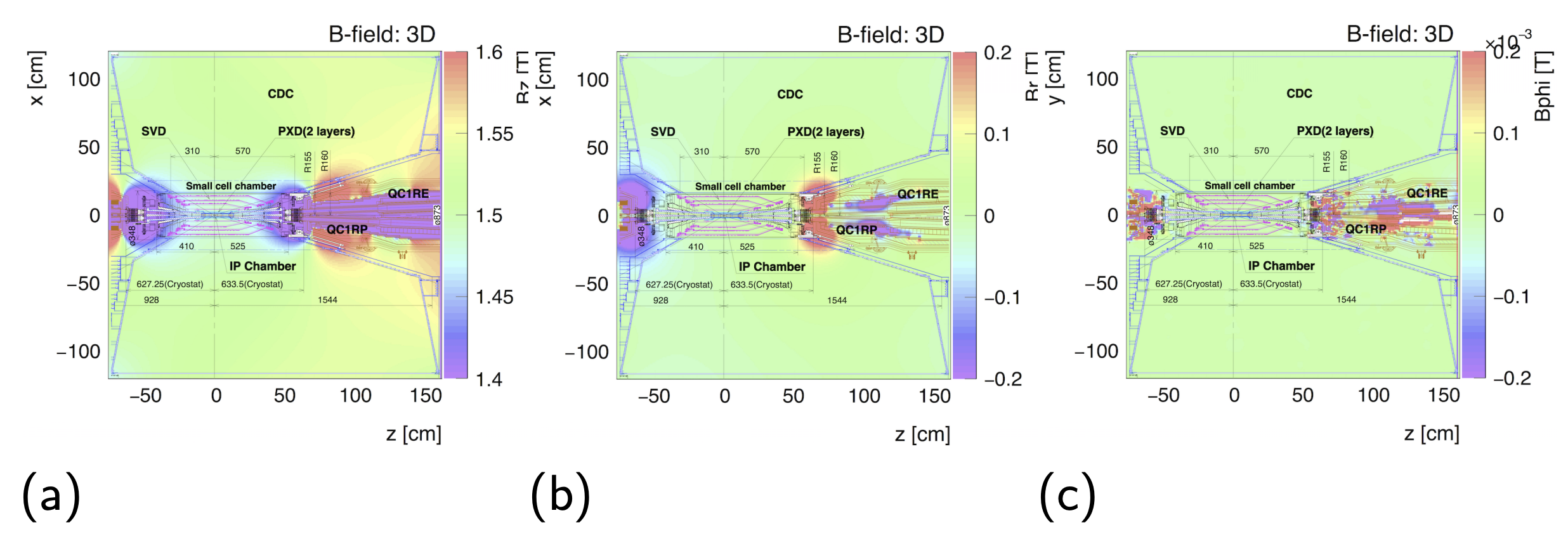
Operating electronics within the Belle II detector volume presents numerous engineering challenges. The electronics must function not only in a harsh radiation environment [8] but also within a strong longitudinal magnetic field of approximately 1.5 T [9]. To mitigate radiation effects such as Single Event Upset (SEU) and Single Event Latch (SEL), techniques for the RFSoC are provided by AMD UG584 user guide[10]. Data on operating RFSoC in such extremely high magnetic fields are unavailable, introducing a project risk when considering RFSoC as a viable solution for the Belle II upgrade. Before RFSoC can be deemed a viable solution as a high-speed digitizer for the Belle II upgrade post-LS2, validation is necessary to ensure that the RFSoC can operate without significant performance degradation. The objective of this paper is to determine whether the RFSoC can operate stably in a strong magnetic field and measure any performance degradation.
2 Hardware
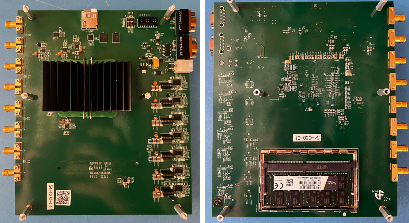
Ideally, this measurement would be performed by placing a commercially available design, such as a development board, into a strong magnetic field. However, finding a commercial development board free of magnetically sensitive components is highly unlikely due to the widespread use of iron-based inductors in DC/DC converters. To address this issue, a custom printed circuit board (PCB) was developed. This PCB features components around the RFSoC that are more resistant to external electromagnetic fields compared to standard commercial boards. Figure 2 shows a photograph of this custom PCB. The board’s dimensions are 152.4 mm by 177.8 mm.
A block diagram of the custom PCB design is shown in Figure 3. The board is powered by a single 5 V power supply, providing power to all the DC/DC converters and linear voltage regulators. An Analog Devices LTC3815 IC, supporting an external inductor, is used for the DC/DC converters. For this DC/DC converter design, an air-core inductor (Abracon AIAC-4125C-R206J-T) was chosen for its superior immunity to external magnetic fields. Unlike iron-based inductors, air-core inductors lack a ferromagnetic core, which significantly reduces their susceptibility to magnetic saturation caused by strong external magnetic fields.
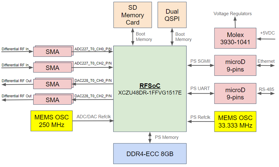
MicroElectroMechanical Systems (MEMS)-based reference oscillators for ADCs, DACs, and the RFSoC’s Processor Side (PS) are used. MEMS oscillators were chosen for their superior immunity to strong external magnetic fields compared to standard quartz oscillators. This is because MEMS oscillators operate on electrostatic rather than electromagnetic principles, making them less susceptible to magnetic interference.
For the RFSoC’s memory, an 8-GB DDR4 SODIMM with Error Correction Code (ECC) support is used. Two boot memory options are available: a dual Quad SPI (QSPI) and an SD memory card.
The RFSoC’s Serial Gigabit Media Independent Interface (SGMII) connects to the Ethernet interface via a microD 9-pin connector, which enables the register configuration and streaming of ADC and DAC waveforms. Another microD 9-pin connector is used for the serial console interface to communicate with the RFSoC’s Linux operating system.
Two of the eight differential ADC channels are connected to SMA connectors, while the other six channels are terminated with 50 Ohms (differential 100 Ohms) via the AC coupling capacitors. Similarly, two of the eight differential DAC channels are connected to SMA connectors, with the other six channels terminated with 50 Ohms (differential 100 Ohms) via the AC coupling capacitors. SMAs are used to provide flexibility for testing through cabling.
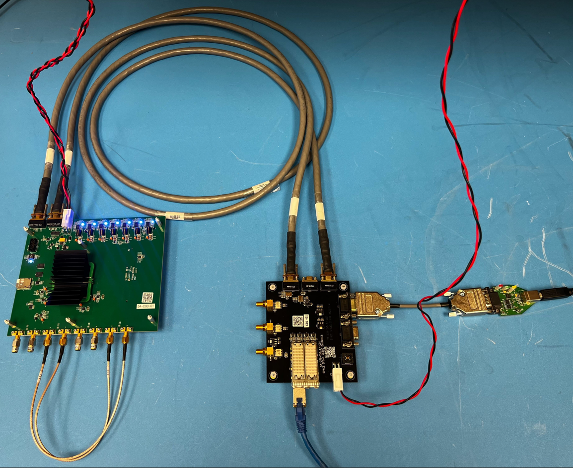
A photograph of the firmware and software development setup before the strong magnetic field testing is shown in Figure 4. This photograph shows hardware setup used during the firmware and software development phase, prior to the actual strong external magnetic field testing. On the left, there is the custom RFSoC board. On the right, there is a custom support board, which converts the serial console interface (RS-485 protocol) to USB, and SGMII to a standard RJ45 Ethernet interface.
3 Firmware
A block diagram of the RFSoC firmware is shown in Figure 5. At the core of the digitization process is the Radio Frequency Data Converter (RFDC) block, a hardened Intellectual Property (IP) within the RFSoC responsible for ADC (Analog-to-Digital Converter) and DAC (Digital-to-Analog Converter) data conversion. The ADC is configured to operate at 5 GSPS across eight channels, receiving analog signals and converting them to digital data. Similarly, the DAC operates at 5 GSPS, converting digital data to analog signals across two channels. The on-board MEMS oscillator provides a 250 MHz reference clock. The RFDC’s internal Phase-Locked Loops (PLLs) convert this 250 MHz reference clock into 5 GHz sampling clocks for the ADC and DAC channels.
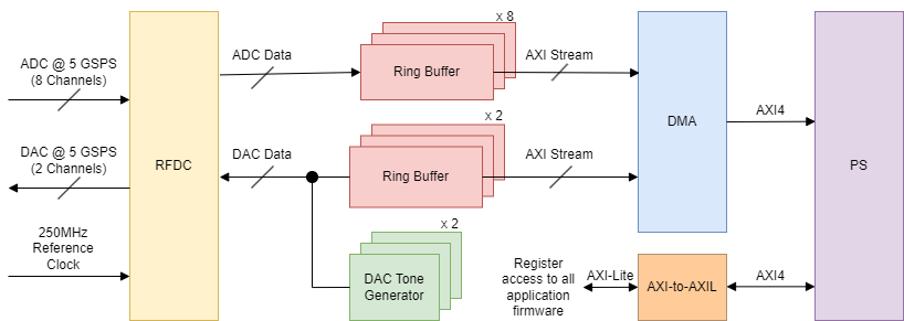
Digital data from the ADC is stored in ring buffers, each with a recording time depth of 13 microseconds. There are eight buffers corresponding to the eight ADC channels. This high-speed data is temporarily stored and periodically read out at a slower rate (a few Hz per buffer). The data from the readout ring buffer is then transmitted as an AXI Stream to the Direct Memory Access (DMA) block via the AXI Stream protocol [12]. Subsequently, the DMA transfers the data over an AXI4 interface to the PS using the AXI4 memory protocol [13].
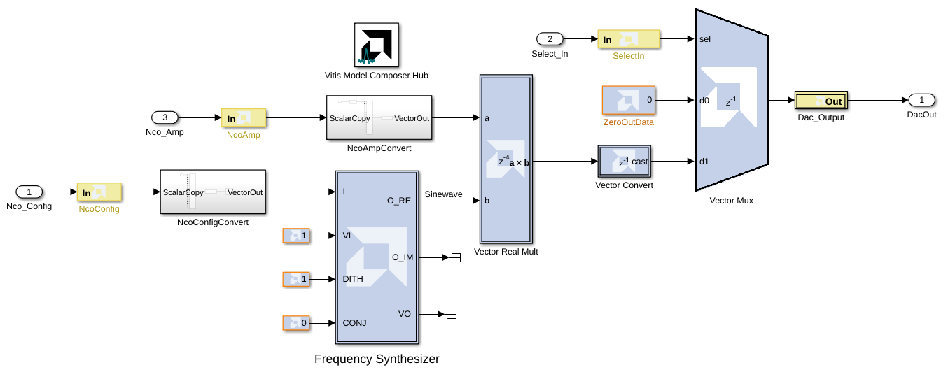
The firmware includes two DAC Tone Generator modules, each capable of internally generating single-tone data for testing purposes. The data generated by these DAC Tone Generator modules is sent to both the RFDC and an additional set of ring buffers, with each buffer corresponding to one of the two DAC channels. A block diagram of a single DAC Tone Generator module is depicted in Figure 6.
Control and register access to all application firmware components is managed via an AXI-Lite interface [13]. A protocol conversion from the PS’s native AXI4 memory interface to an AXI-Lite interface is used.
4 Software
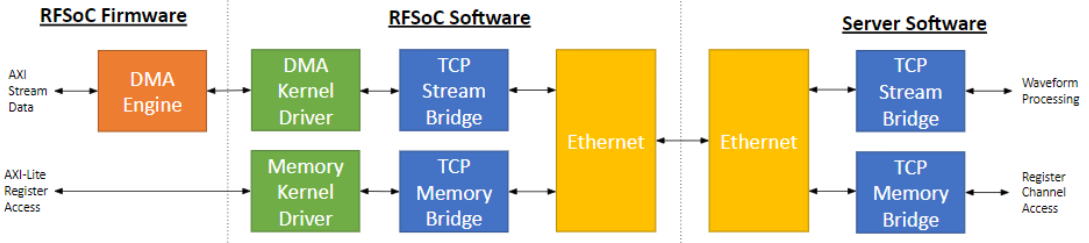
In the architectural diagram shown in Figure 7, the integration of RFSoC firmware, RFSoC software, and server software is outlined. Within the RFSoC firmware domain, the waveforms are relayed to the DMA engine and the associated DMA kernel driver via the AXI Stream interface. Concurrently, AXI-Lite register access is performed through a memory kernel driver, which imposes restrictions on user access to registers outside of the designated application firmware register address space. A TCP stream bridge is used to transform the waveform data into TCP packets that are suitable for Ethernet transmission. Similarly, the TCP memory bridge serves to translate register access communications between the memory kernel driver and the Ethernet-based TCP interface. On the server side, the equivalent TCP stream and memory bridges work to encode and decode the TCP packets back into interfaces that are compatible with the native run control software. The RFSoC uses Petalinux (version 6.1.30-xilinx-v2023.2) to manage its Linux kernel operations.
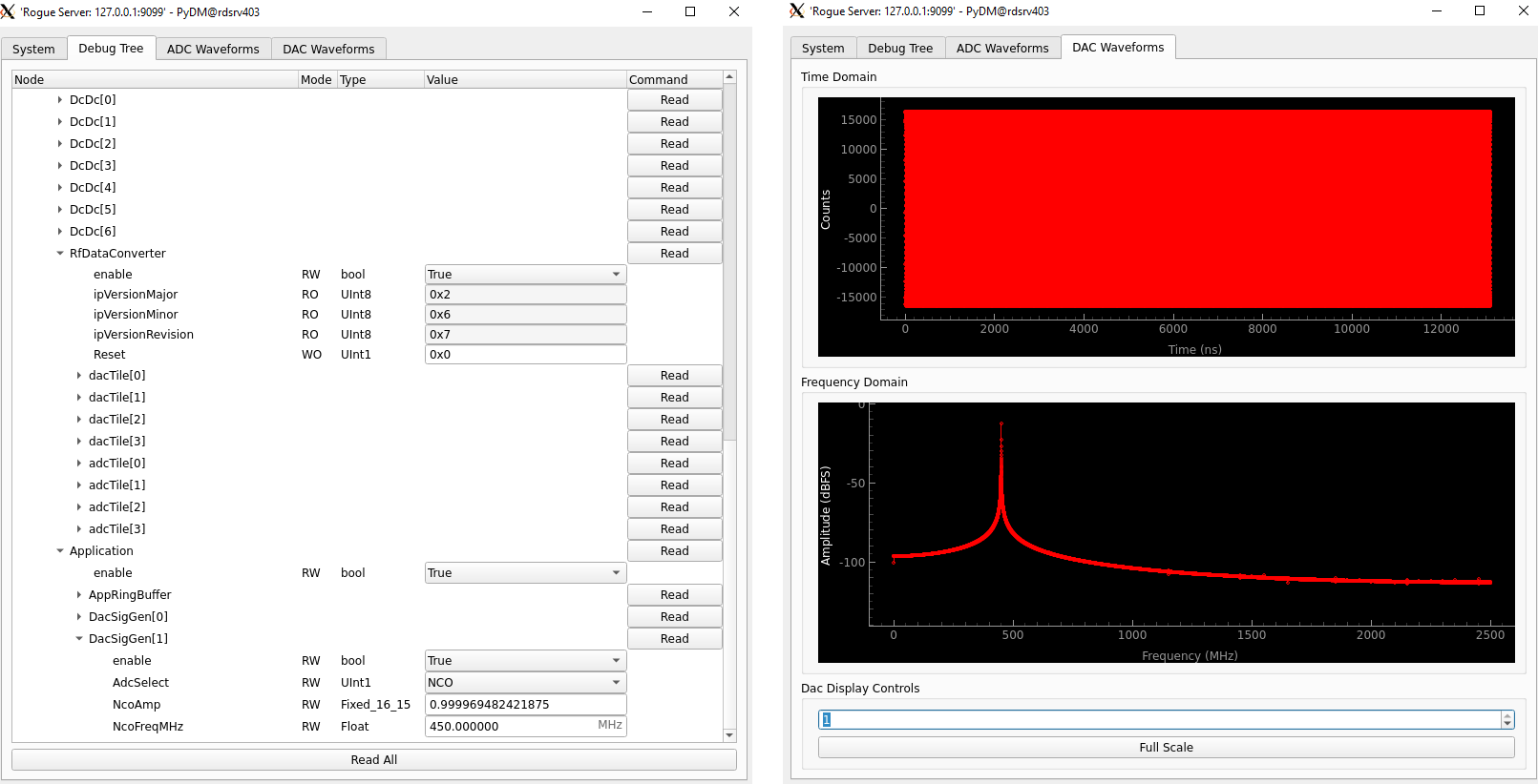
The control software used in this testing, referred to as Rogue, is tailored for the swift prototyping and deployment of experimental setups. It supports execution in a hybrid Python/C++ mode or exclusively in C++. The software is compatible with x86-64, ARM32, and ARM64 platforms [15]. Rogue control software runs on both the RFSoC and the rack server, sharing a library for the TCP stream and memory bridges. Within Rogue, the application register mapping on the RFSoC is established through Python classes. Additionally, the system incorporates a Python class dedicated to transforming the raw byte array into a 16-bit numpy array, facilitating the analysis and processing of waveform data. A graphical user interface (GUI) has also been developed using the Rogue platform to enable live-display monitoring of ADC/DAC waveforms and registers, as shown in the example screenshot in Figure 8. This GUI leverages the Python Display Manager (PyDM), which is based on PyQt, to create user interfaces for control systems [16].
5 Testing
5.1 Magnetic Field Setup
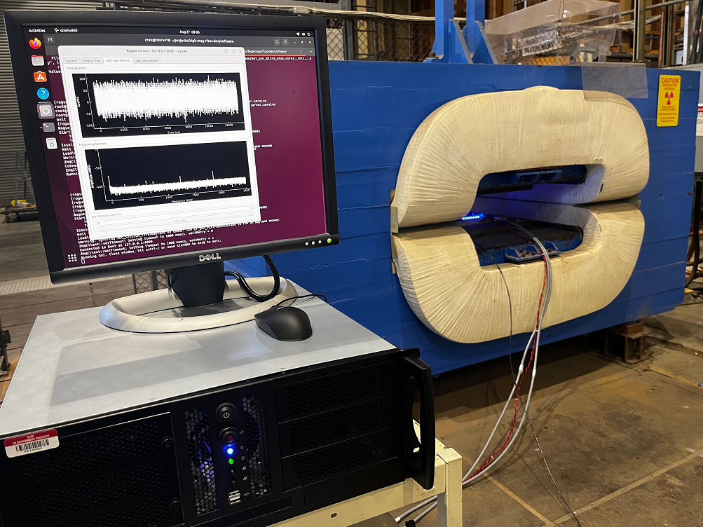
A photograph of the test setup is shown in Figure 9. The magnet used, referred to as "Big Blue," is located at the SLAC National Accelerator Laboratory in the Heavy Fabrication Building (Building 026). The magnet measures 2.5 meters wide, 0.9 meters deep, and 1.3 meters high, with an approximate weight of 23 metric tons. It can generate a uniform magnetic field of up to 1.25 T in the center of the gap, where the RFSoC board was positioned. Although the testing was ideally meant to be conducted at a field strength of 1.5 T, matching the conditions within the Belle II detector, the SLAC magnet’s maximum field strength was limited to 1.25 T due to power supply and cooling limitations. The support board and server were connected via cables, positioned outside the magnet, in an area with minimal stray magnetic fields. During each magnetic field increment, waveforms were collected, and all status registers in the RFSoC were logged. Accurate magnetic field readings for each step were provided by a Group 3 DTM-141 Digital Teslameter module, with its probe placed in the magnet’s gap.
5.2 Loopback Testing in Magnetic Field
SMA loopback cables were connected from the differential pair of DAC channel 1 to the differential pair of ADC channel 6. DAC channel 0 and ADC channel 7 were terminated using 50 Ohm SMA terminators, while all other ADC and DAC channels were already terminated onboard. A 400 MHz single tone was generated on DAC channel 1 via firmware (refer to Figure 6) and measured by ADC channel 6 to characterize the RFSoC digitization performance during magnet testing. The Fast Fourier Transform (FFT) plots for DAC channel 1 and all ADC channels at 1.25 T are shown in Figure 10.
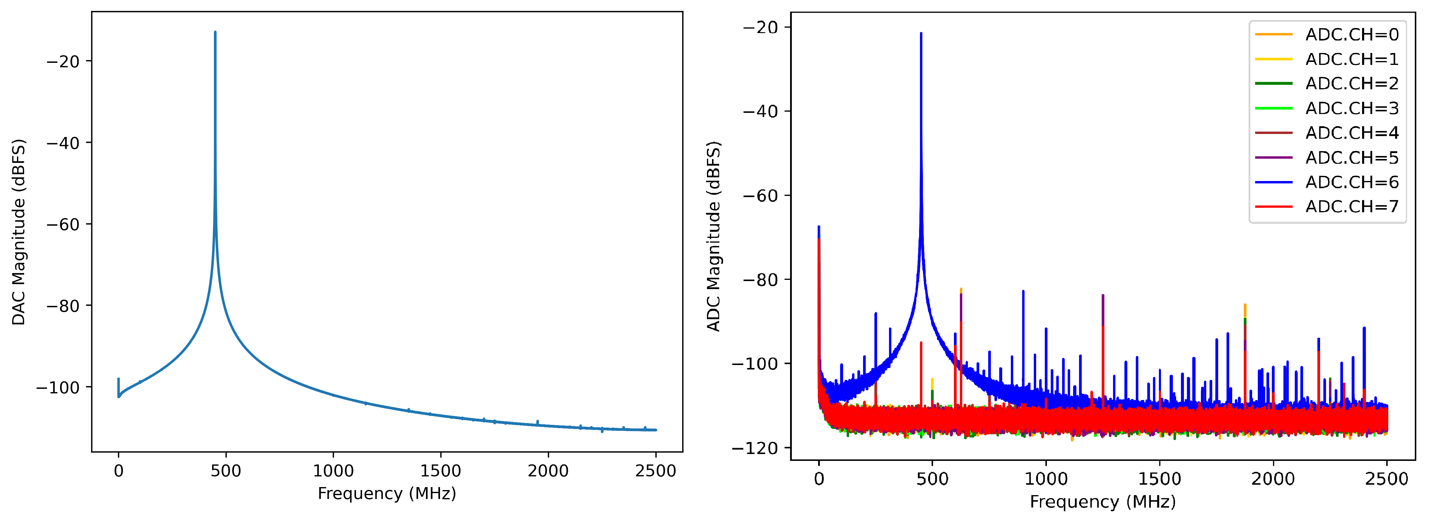
Spurious-Free Dynamic Range (SFDR) is an effective metric for characterizing ADC performance, as it measures the ADC’s ability to distinguish the desired signal from the largest spurious signal above the noise floor. This metric reflects the ADC’s precision and dynamic range in environments where spurious signals and noise can interfere with accurate signal representation. The SFDR is determined by calculating the difference between the power of the fundamental signal and that of the largest spurious signal. The largest spurious signal, observed at 800 MHz, was identified as the second harmonic of the fundamental tone on ADC channel 6. The next largest noise spurs, observed across all ADC channels and shown in Figure 10, were located at 625 MHz, 1.25 GHz, and 1.875 GHz. These spurs are attributed to the 8-fold interleaved structure of the integrated ADCs in the RFSoC [17, 18].
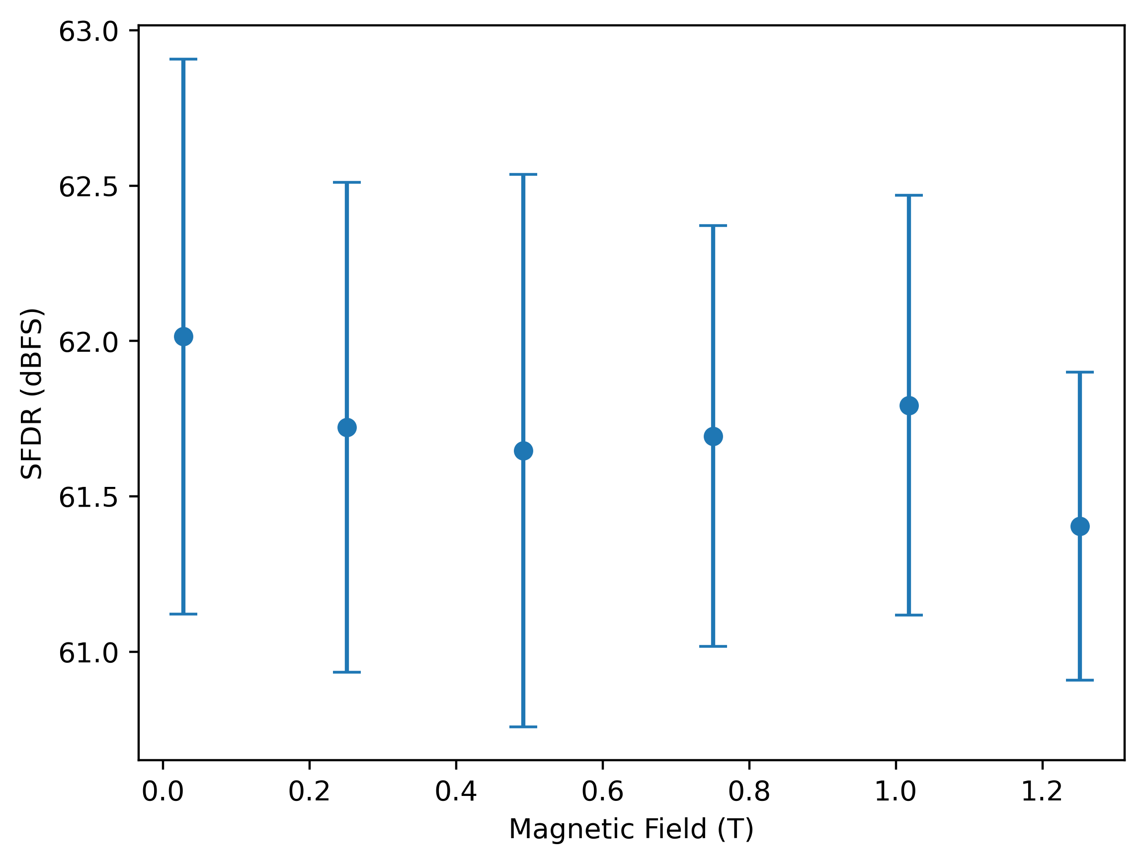
ADC waveforms were collected at approximately 0.25 T magnetic field increments, with 100 waveforms recorded per channel per step. ADC channel 6, which received the single-tone signal from the DAC, was used to calculate the SFDR for each magnetic field step. A plot of SFDR versus magnetic field is presented in Figure 11. The SFDR remained consistent across the entire magnetic field range, demonstrating that the ADC and DAC exhibit significant immunity to external strong magnetic fields.
5.3 Non-orthogonal Magnetic Field Operation
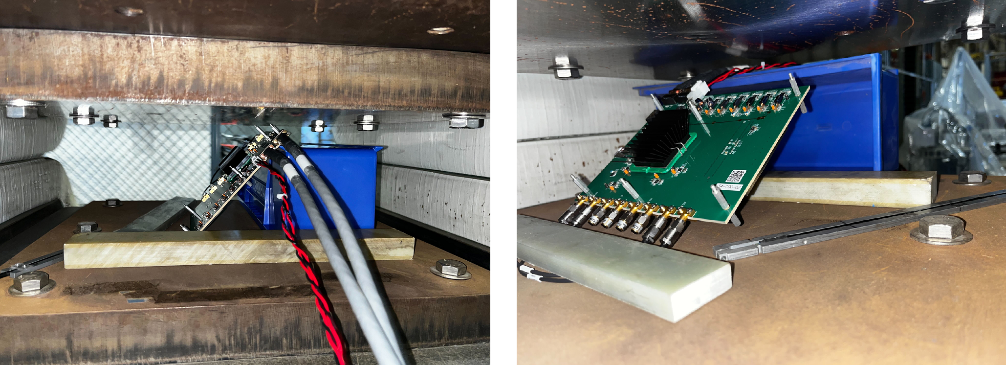
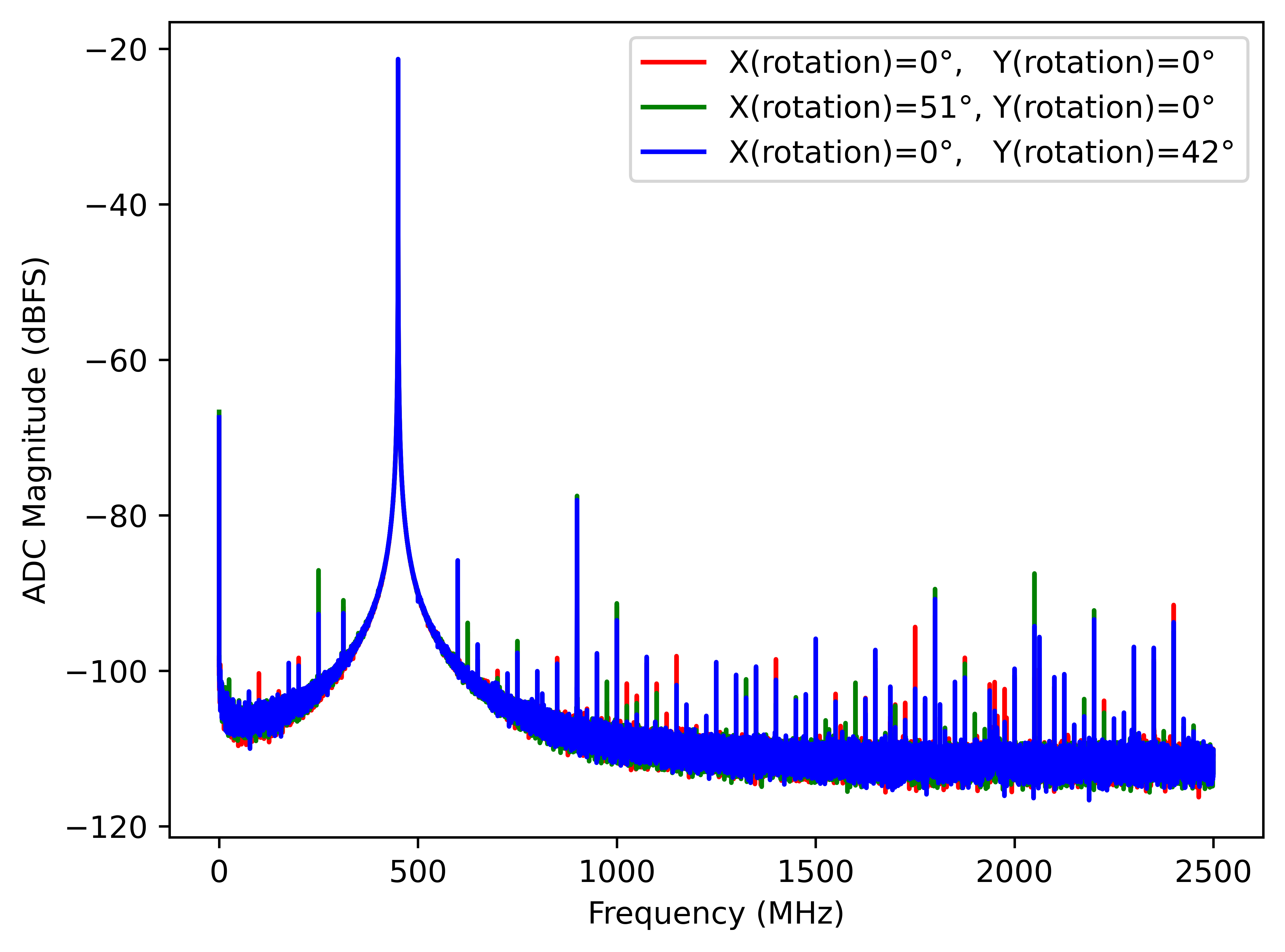
For the testing described in Section 5.2, the magnetic field was oriented orthogonally to the RFSoC and PCB. However, if the RFSoC is to be used in the Belle II detector, it will need to operate in non-orthogonal field configurations. Therefore, the RFSoC board was tested in two additional configurations at 1.25 T, as shown in Figure 12. In the first non-orthogonal configuration, the board was rotated about its X-axis by 51∘. In the second configuration, the board was rotated about its Y-axis by 42∘. Ideally, these rotations would have been 90∘, but the physical dimensions of the board and its cabling prevented this. Consequently, the rotations achieved that represent the maximum feasible configurations within the magnet’s gap.
For each of these non-orthogonal field configurations, 100 waveforms per channel were collected at 1.25 T, and compared with the orthogonal configuration described in Section 5.2. An FFT plot for ADC channel 6, overlaying the three configurations, is presented in Figure 13. An SFDR of approximately 62 dBFS was measured in both non-orthogonal field configurations, comparable to the SFDR observed in the orthogonal configuration. This indicates that the RFSoC has significant immunity to strong external magnetic fields, even at different incident angles of the magnetic field.
5.4 RFSoC Power Draw Monitoring
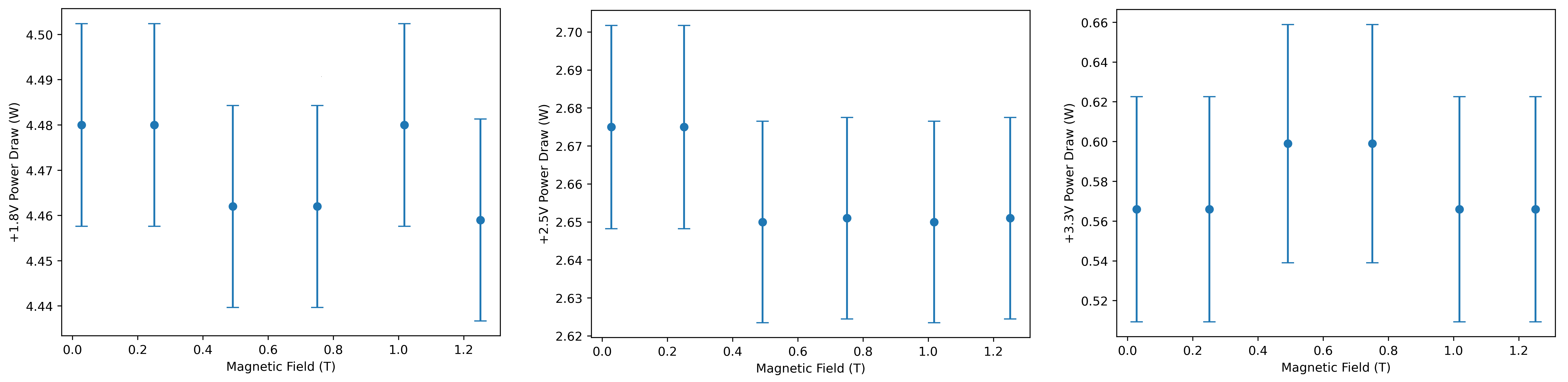
For the DC/DC converters, Analog Devices’ LTC3815 ICs were used. This IC has a Power Management Bus (PMBus) interface that was connected to the RFSoC’s I/O. This PMBus provides useful diagnostics on the DC/DC converters, such as voltage, current, and power for both the input and output of the voltage regulator, with approximately 1% accuracy. After each magnet step and collecting ADC waveforms, a dump of all the firmware status registers was logged, including the PMBus registers, for offline analysis.
The DC/DC 1.8V voltage supply is regulated to 0.925V by linear voltage regulators for the RFSoC’s analog core voltages: ADC_AVCC and DAC_AVCC. The DC/DC 2.5V voltage supply is regulated to 1.8V by linear voltage regulators for the RFSoC’s analog auxiliary voltages: ADC_AVCCAUX and DAC_AVCCAUX. The DC/DC 3.3V voltage supply is regulated to 3.0V by a linear voltage regulator for the for the RFSoC’s DAC output driver supply (DAC_AVTT). As shown in Figure 14, the power drawn from these three rails, which supply the RFSoC’s ADC and DAC circuits, remains fairly consistent across the entire tested magnetic field range. This consistency shows no evidence that the RFSoC’s ADC and DAC circuits susceptible to external magnetic fields.
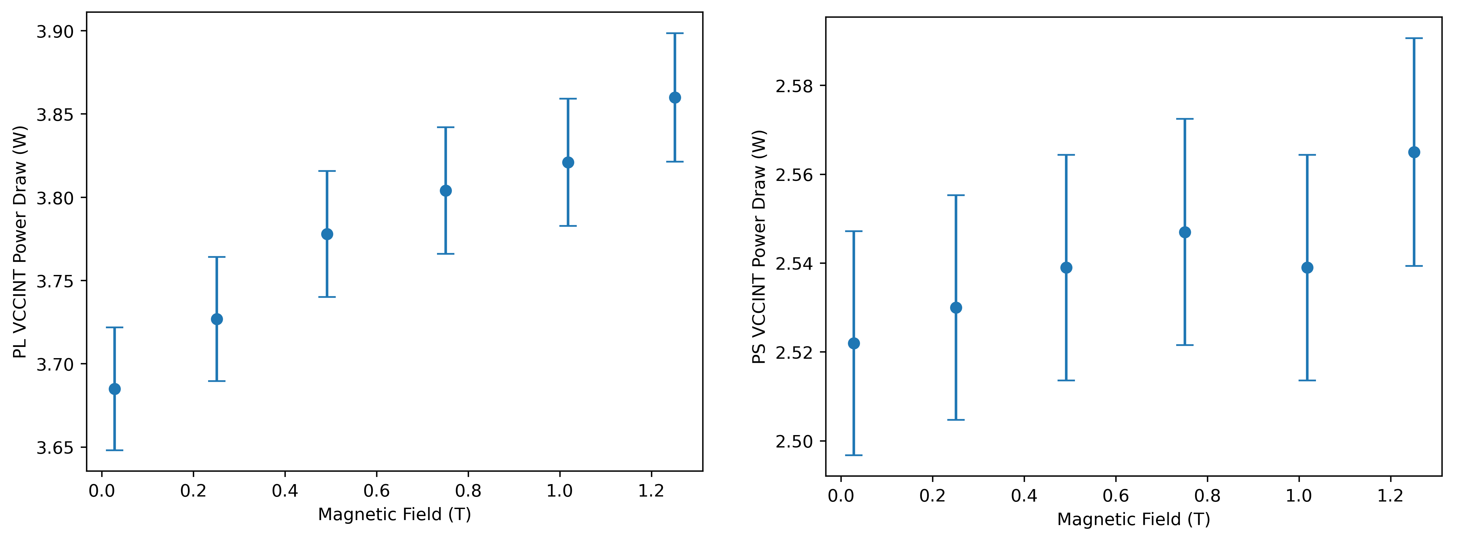
The power draw from the PL core voltage supply (Programmable Logic (VCCINT)) and the PS core voltage supply (Processor Side (VCCINT)), both regulated at 0.85V by separate DC/DC converters, are shown in Figure 14. While the PS VCCINT power draw remains fairly consistent across the entire tested range of magnetic fields, a linear dependency of the PL VCCINT power draw on strong external magnetic fields is evident. However, the increase in power draw is only about 5% across this range of magnetic fields, which is minimal enough not to have a significant impact on the operation of the RFSoC in strong magnetic fields.
5.5 Boot Memory Testing
With a magnetic field set at 1.25 T and the RFSoC initially in the power-down state, it was powered up using the SD memory card to boot. No software errors were observed in the PetaLinux boot logs of the RFSoC. No issues were observed when running the software using the Rogue software GUI, and the live waveforms displayed appeared similar to those from previous testing, with an SFDR of approximately 62 dBFS.
Subsequently, both the magnet and the RFSoC were powered down to change the DIP switch on the RFSoC board for QSPI boot. Once the magnetic field was ramped up to 1.25 T again, the RFSoC board was powered on for QSPI boot. Similar to the behavior observed during the boot from the SD memory, no software errors were noted in the boot log, and the waveform behavior was similar to that observed previously.
6 Summary
The RFSoC was identified as a potential solution for the Belle II detector’s upgrade, which requires its operation in a high magnetic field environment. To assess its viability, a custom RFSoC board was designed with peripheral components selected for their resistance to magnetic susceptibility, including air-core inductors and MEMS-based oscillators. Using this custom board, the performance of an RFSoC operating within a 1.25 T magnetic field was evaluated.
We conducted testing by placing the RFSoC board within a strong magnetic field and performing a series of measurements to evaluate its performance. The tests included loopback testing of the RFSoC’s ADC and DAC channels, which demonstrated that the SFDR remained consistent across the entire magnetic field range. This consistency indicated that the ADC and DAC circuits of the RFSoC were largely unaffected by the strong external magnetic field. We also rotated the RFSoC board in non-orthogonal magnetic field configurations, further confirming its robustness against magnetic field variations.
Power consumption of the RFSoC was monitored throughout the tests, revealing minimal impact on power draw across different magnetic field strengths. Additionally, the SD memory card and QSPI boot options were tested, and no error messages in the boot log or abnormal behavior were observed.
The results indicate that the RFSoC can operate reliably within a 1.25 T magnetic field without significant performance degradation, which is promising for its potential use in Belle II. Ideally, this evaluation would have been conducted in a 1.5 T field, since that is the magnetic field strength used in the Belle II detector volume. However, the positive results obtained at 1.25 T suggest that the RFSoC is likely to operate at 1.5 T as well. Further testing at 1.5 T will be necessary to conclusively confirm the RFSoC’s suitability for the Belle II upgrades.
7 Acknowledgements
Work supported by the U.S. Department of Energy, under contract number DE-AC02-76SF00515. Also special thanks to Scott Anderson at SLAC National Accelerator Laboratory for his invaluable assistance in operating the magnet during the testing process.
References
- [1] A. Abashian, et al., "The Belle Detector", Nucl. Instr. and Meth. A 479 (2002) 117–232. http://dx.doi.org/10.1016/S0168-9002(01)02013-7.
- [2] F.Forti for Belle II Collaboration, "The Belle II Detector Upgrades Conceptual Design Report", KEK, Report No. BELLE2-REPORT-2023-001 (2023)
- [3] Aggarwal, Latika et al., "Snowmass White Paper: Belle II physics reach and plans for the next decade and beyond", Belle-II Collaboration, arXiv:2207.06307, 2022.
- [4] Dmitri Kotchetkov, et al., "Front-end electronic readout system for the Belle II imaging Time-Of-Propagation detector", Nucl. Instr. and Meth. A 941 (2019) 447-460, https://doi.org/10.1016/j.nima.2019.162342.
- [5] I. Mostafanezhad, "Overview of KLM Electronics", Belle II Summer School at PNNL, August 2015
- [6] "White Paper: An Adaptable Direct RF-Sampling Solution", AMD WP489 (v1.1) February 20, 2019, https://docs.amd.com/v/u/en-US/wp489-rfsampling-solutions
- [7] "Technical Overview of AMD RFSoC Technology", AMD Technical Documentation, https://www.xilinx.com/products/silicon-devices/soc/rfsoc.html
- [8] Higuchi et al, "Radiation tolerance of readout electronics for Belle II" 2012 JINST 7 C02022, https://doi.org/10.1088/1748-0221/7/02/C02022
- [9] Y. Arimoto et al.,"Three Dimensional Field Analysis for Final Focus Magnet System at SuperKEKB", Proceedings, 5th International Particle Accelerator Conference, WEPRI086 (2014).
- [10] "Using LVAUX Mode in XQ Ruggedized UltraScale+ Devices for Airborne Systems Design Guide (UG584)", AMD Technical Documentation, https://docs.amd.com/r/en-US/ug584-xq-lvaux-mode
- [11] Szymon Bacher, "Investigation of magnetic field inside Belle II spectrometer", KEK, Talk No. BELLE2-TALK-CONF-2020-007 (2020) https://docs.belle2.org/record/1854
- [12] AMBA 4 AXI4-Stream Protocol Specification, ARM IHI 0051A (ID030610)
- [13] AMBA AXI and ACE Protocol Specification, ARM ARM IHI 0022E (ID033013)
- [14] "Technical Overview of Vitis Model Composer", AMD Technical Documentation, https://www.xilinx.com/products/design-tools/vitis/vitis-model-composer.html
- [15] Rogue Software Framework, https://slaclab.github.io/rogue
- [16] PyDM: a PyQt-based framework for building user interfaces for control systems, https://slaclab.github.io/pydm
- [17] AMD Inc., “Zynq UltraScale+ RFSoC RF Data Converter v2.6 Gen 1/2/3/DFE LogiCORE IP Product Guide (PG269)” v2.6, (2022). https://docs.amd.com/r/en-US/pg269-rf-data-converter
- [18] Liu, C., Jones, M. E., and Taylor, A. C., “Characterizing the performance of high-speed data converters for RFSoC-based radio astronomy receivers,” Monthly Notices of the Royal Astronomical Society 501, 5096–5104 (12 2020). https://doi.org/10.1093/mnras/staa3895