Magnetic metamaterials by ion-implantation
Abstract
We present a method for the additive fabrication of planar magnetic nanoarrays with minimal surface roughness. Synthesis is accomplished by combining electron-beam lithography, used to generate nanometric patterned masks, with ion implantation in thin films. By implanting 56Fe+ ions, we are able to introduce magnetic functionality in a controlled manner into continuous Pd thin films, achieving 3D spatial resolution down to a few tens of nanometers. Our results demonstrate the successful application of this technique in fabricating square artificial spin ice lattices, which exhibit well-defined magnetization textures and interactions among the patterned magnetic elements.
Magnetic nanoarrays - metamaterials - have gained significant attention in recent years, both as systems of fundamental interest [1, 2, 3, 4, 5], and as promising candidates for applications in neuromorphic computing [6, 7, 8], as well as in magnonic and spintronic devices [9, 10, 11]. The scalability and versatility of these systems have opened new pathways for exploring emergent physics [1, 3] and expanding their potential applications. However, the topography of these magnetic nanoarrays, resulting from the nanopatterning process, can present significant challenges. A notable example is the observed strong structure-related photon scattering, which can obscure scattering resulting from magnetic ordering in the arrays [12]. Given that the photon scattering properties of these systems could play a crucial role in information technology applications [13], or in x-ray metasurfaces for manipulating photon angular and orbital momentum [12], it is essential to explore methods for developing truly planar arrays that maintain flexibility in material selection and precise spatial control.
To this end, ion-beam techniques offer a promising pathway. Previously, ion-beam irradiation by means of Focused Ion Beam (FIB) was used for creating arrays without a significant topography. FIB is a commonly used technique, where a beam of focused ions is directed towards a target and a pattern can be created by sweeping of the beam. By adjusting the FIB fluence, it is possible to reduce the topography of the patterns to some extent [14]. Another approach to creating flat magnetic metamaterials involves ion-implantation through a physical mask. Since the pioneering work of Chappert et al. [15], magnetic patterns have been engineered by locally altering the magnetic properties of a film via ion implantation [16, 17, 14, 18, 19]. However, it was not until recently that magnetic features were additively implanted [20]. Employing readily available masks, flat magnetic patterns were successfully created, although the feasible designs remain constrained by the limitations of the available mask configurations.
In this work, we focus on fabricating a patterned mask on top of a film through which magnetic patterns can be created using ion-implantation. We achieve this, combining the pattern design flexibility of modern nanolithography techniques with standard ion-implantation methods. In the present work, 56Fe+ ions are implanted into a Pd film through a Cr patterned mask, yielding flat ferromagnetic FexPd100-x (where stands for at.%) nanostructures embedded into the Pd matrix. The pre-patterned mask enables the design of architectures with geometries and shapes that cannot be achieved with standard masks found in market, while the dimensions of the building blocks can be reduced to the scale of a few tens of nanometers. The specific magnetic metamaterial architecture of choice is an Artificial Spin Ice (ASI) lattice due to the wide interest it has attracted and the potential to be implemented in applications [5, 1, 3, 21, 13, 12, 8].
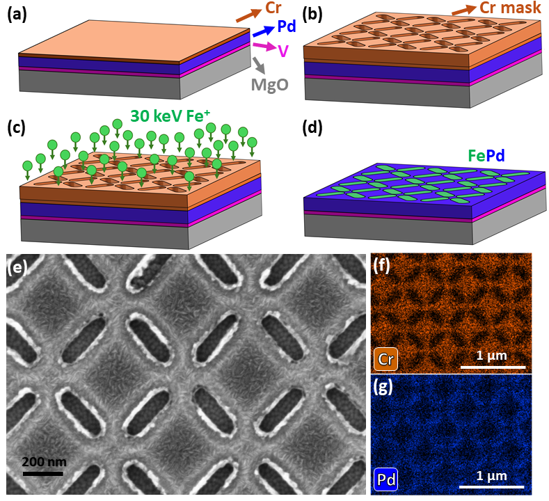
A 600 Å Pd film with a 50 Å V film adhesion layer was deposited on a MgO substrate using DC magnetron sputtering. Subsequently, 60 Å Cr were deposited on top of the Pd film by thermal evaporation, to act as a protection layer during the Fe+ implantation (Fig. 1 (a)). A patterned Cr mask was prepared on top of the film by means of electron-beam lithography (EBL). More details are presented in the Supplementary Material. The pre-patterned mask consists of stadium-shaped holes with length of 290 nm, width of 80 nm and depth of 60 nm placed in a square ASI lattice with periodicity 480 nm (Fig. 1 (b)). Scanning Electron Microscope (SEM) and Energy Dispersive Spectroscopy (EDS) images of the film with the pre-patterned mask on top are shown in Fig.1 (e) and (f,g), confirming a well-formed mask structure and full Cr removal at the hole sites.
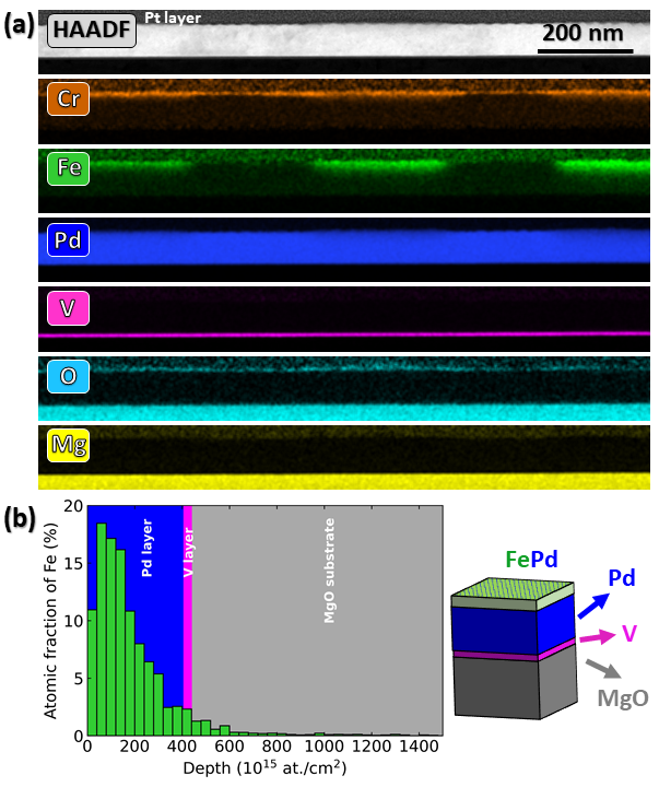
Using this Cr mask, the nanopattern was deposited into the Pd film by 56Fe+ implantation, with an energy of 30 keV and nominal fluence of 41016 ions/cm2 (Fig. 1 (c)). The selected fluence is low enough to ensure that the sample is not heated significantly, thereby hindering diffusion. This step was followed by the chemical removal of the Cr mask (Fig. 1 (d)). Details can be found in the Supplementary Material. Fig. 2 (a) shows a SEM image of the implanted pattern, where FexPd100-x stadium-shaped structures of length 300 nm and width 100 nm have been created into the Pd film. The final dimensions of the implanted nanostructures are slightly larger than the corresponding holes of the mask due to lateral straggling as Fe+ ions penetrate the Pd film. The surface topography of the sample was mapped performing Atomic Force Microscopy (AFM) in contact mode. The AFM image in Fig. 2 (b) manifests that the implanted nanostructures have low surface roughness. Factors that contribute to the roughness are the sputtered Cr atoms during implantation and the implanted Fe atoms in the Pd film. By extracting height profiles across a nanostructure from the AFM images (Fig. 2 (c)), we conclude that the roughness is on the order of 4–5 nm. Cross-sectional Transmission Electron Microscopy (TEM) EDS analysis were performed on the implanted patterns, as shown in Fig. 3 (a). The TEM image confirms the low surface roughness of the implanted regions. The EDS spectrum displays a signal for Fe with a width of 300 nm along the long-axis of the implanted elements, detected in the Pd film. This observation confirms Fe implantation according to the pre-patterned mask design. The intensity of the Fe signal is strong close to the sample surface and decreases towards the substrate, indicating that the Fe has a concentration depth-profile, as expected [22]. This concentration-depth profile confirms the limited diffusion of Fe into the Pd film. Furthermore, some Cr is detected in the Fe implanted areas, highlighting that some Cr atoms have been implanted due to knock-on collisions as a side effect of the implantation process. To determine the Fe depth-profile of the sample, Ion Beam Analysis (IBA) in the form of Time-of-Flight Elastic Recoil Detection Analysis (ToF – ERDA), was performed on a continuous film that was prepared and implanted next to the masked sample. This measurement confirmed that Fe has indeed a concentration profile in the Pd film with its peak to be close to the sample surface and at around 18.4% atomic concentration for the selected fluence (Fig. 3 (b)).

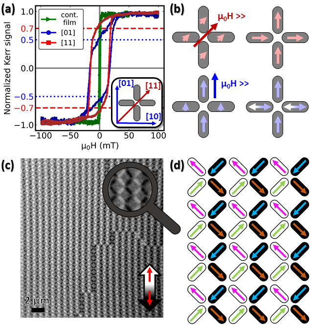
The magnetic properties of the implanted films were studied using the Longitudinal Magneto-Optical Kerr Effect (LMOKE). Magnetic hysteresis loops were recorded at room temperature and are shown in Fig. 4 (a), for an implanted continuous film and ASI array. The hysteresis loop of the continuous film exhibits a normalized remanence magnetization below 1. This decreased remanence might be a consequence of Cr implantation and possible antiferromagnetic contribution due to that [23]. Similar effects have been reported for NiFe alloys implanted with Cr+ [24, 25]. For the implanted ASI structure, the external magnetic field was applied in two directions, parallel to the [01] and parallel to the [11] directions (see inset Fig. 4 (a)). When the array reaches the saturation state, the magnetic moments are aligned in the field direction (see Fig. 4 (b) left). After the removal of the field (remanent state), the shape of the elements forces the magnetization to be parallel with the long-axis of the elements, confining it in only two possible orientations. This restriction leads to a fully ordered remanent state after applying a magnetic field along the [11] direction (Fig. 4 (b) top right), yielding ideally a normalized remanent magnetization, with respect to the saturation magnetization, equal to . Similarly, a return to the remanent state after the application of a field along the [01] direction, leads to a full order for the elements parallel to [01] direction and a random order for the elements parallel to [10] direction (Fig. 4 (b) bottom right), yielding a normalized remanent magnetization equal to 0.5. This hysteretic behavior of the patterned array highlights the single magnetic domain structure of the implanted nanoelements as well as their collective behavior. Conventional lithographic ASI lattices exhibited comparable behavior [26, 27].
To directly illustrate the magnetic state of the implanted nanostructures, photoemission electron microscopy, employing x-ray magnetic circular dichroism (PEEM-XMCD) experiments were performed at the ESM (21-ID-2) beamline at the NSLS-II synchrotron and at the CIRCE (bl24) beamline at the ALBA synchrotron [28]. The experiments were performed on two sets of samples which were prepared as described above (for more details, see Supplementary Material), and implanted in ASI lattices with a range of element dimensions and lattice periodicities. The 30 keV Fe+ ions were implanted with a nominal fluence of 41016 ions/cm2 for one sample and 2.71016 ions/cm2 for the second sample. The PEEM-XMCD imaging was performed at room temperature in the absence of any external magnetic field, with a photon energy tuned to the Fe L3-edge (707 eV). A representative PEEM-XMCD image of an implanted ASI lattice is shown in Fig. 4 (c). The nanostructures are clearly displayed with white or black color, confirming their single magnetic domain state. Furthermore, the observed magnetic contrast confirms that the ASI lattice has obtained antiferromagnetic order (Type I), being the ground state of the square ASI lattice [29]. This order establishes the presence of sufficiently strong magnetic interactions between the implanted nanostructures. The formation of these extended domains, hints also towards an effective thermalization and relaxation process taking place during implantation, similar to temperature protocols which have been reported previously [30, 31].
The magnetic metamaterial fabrication process detailed here results in flat nanoarrays, which can be especially beneficial for magnetically controlled flat optical devices. [12, 32]. This approach has the potential to enhance the steering of light beams by means of diffraction angles and energy range, offering a significant improvement over methods that rely on magnetic domain structures in yttrium-iron garnets [32] or rare-earth transition metal alloys [33]. An additional advantage of this technique is the flexibility it provides in selecting the combination of implanted ion species and target materials. This flexibility enables the creation of material combinations that are not favoured in terms of thermodynamical stability, thereby expanding the range of possible materials for use in these applications. Moreover, the target material plays a crucial role in determining the overall magnetic properties of the metamaterials. In this work, palladium was chosen for its high magnetic susceptibility [34, 35]. As a consequence, palladium obtains a strong induced magnetic moment from iron and exhibits ferromagnetic properties in a region that can extend several nanometers from the Fe interface [35]. This induced polarization effectively "smoothens” the edges of the magnetic implanted nanostructures. Finally, this magnetic polarization effect enables interactions between the magnetic elements that can be tailored in ways that go beyond the capabilities of previous approaches, which were limited by nanolithography and geometric constraints[36, 37, 38]. Another possible area that can benefit from this technique is magnonic circuits. A flat ferromagnetic architecture in a non-ferromagnetic matrix can be an ideal candidate for fabricating magnonic busses. The lack of height step between the ferromagnetic and non-ferromagnetic parts could facilitate the patterning of the antennas needed in the magnonic circuits [39].
The authors would like to thank Johan Oscarsson and Mauricio Sortica at the Uppsala Tandem Laboratory for help with ion implantations. The authors are thankful for an infrastructure grant by VR-RFI (grant number 2019-00191) supporting the accelerator operation. The authors also acknowledge support from the Swedish Research Council (project no. 2019-03581). CV would like to thank David Muradas, Dr. Daria Belotcerkovtceva and Dr. Gopal Datt for fruitful discussions. CV further gratefully acknowledges financial support from the Colonias-Jansson Foundation, Thelin-Gertrud Foundation, Liljewalch and Sederholm Foundation. We acknowledge Myfab Uppsala for providing facilities and experimental support. Myfab is funded by the Swedish Research Council (2020-00207) as a national research infrastructure. We would also like to thank Associate Professor Venkata Kamalakar Mutta for providing us chemicals for the process. The PEEM-XMCD experiments were performed at CIRCE (bl24) beamline at ALBA Synchrotron with the collaboration of ALBA staff. M.F. acknowledges support from MICIN through grant number PID2021-122980OB-C54. This research used resources of the National Synchrotron Light Source II and the Center for Functional Nanomaterials, U.S. Department of Energy (DOE) Office of Science User Facilities operated for the DOE Office of Science by Brookhaven National Laboratory under Contract No. DE-SC0012704. The authors are deeply grateful for the support from ReMade@ARI, funded by the European Union as part of the Horizon Europe call HORIZON-INFRA-2021-SERV-01 under grant agreement number 101058414 and co-funded by UK Research and Innovation (UKRI) under the UK government’s Horizon Europe funding guarantee (grant number 10039728) and by the Swiss State Secretariat for Education, Research and Innovation (SERI) under contract number 22.00187.
DATA AVAILABILITY
The data that support the findings of this study are available from the corresponding authors upon reasonable request.
References
- Heyderman and Stamps [2013] L. J. Heyderman and R. L. Stamps, J. Phys.: Condens. Matter 25, 363201 (2013).
- Gilbert et al. [2016] I. Gilbert, C. Nisoli, and P. Schiffer, Physics Today 69, 54 (2016).
- Nisoli et al. [2017] C. Nisoli, V. Kapaklis, and P. Schiffer, Nature Physics 13, 200 (2017).
- Rougemaille and Canals [2019] N. Rougemaille and B. Canals, Eur. Phys. J. B 92, 62 (2019).
- Skjærvø et al. [2020] S. H. Skjærvø, C. H. Marrows, R. L. Stamps, and L. J. Heyderman, Nature Reviews Physics 2, 13 (2020).
- Papp et al. [2021] A. Papp, W. Porod, and G. Csaba, Nature Communications 12, 6422 (2021).
- Jensen et al. [2018] J. H. Jensen, E. Folven, and G. Tufte, The 2018 Conference on Artificial Life , 15 (2018).
- Gartside et al. [2022] J. C. Gartside, K. D. Stenning, A. Vanstone, H. H. Holder, D. M. Arroo, T. Dion, F. Caravelli, H. Kurebayashi, and W. R. Branford, Nature Nanotechnology 17, 460 (2022).
- Gliga et al. [2013] S. Gliga, A. Kákay, R. Hertel, and O. G. Heinonen, Physical Review Letters 110, 117205 (2013).
- Iacocca et al. [2016] E. Iacocca, S. Gliga, R. L. Stamps, and O. Heinonen, Physical Review B 93, 134420 (2016).
- Marrows et al. [2024] C. H. Marrows, J. Barker, T. A. Moore, and T. Moorsom, npj Spintronics 2, 12 (2024).
- Woods et al. [2021] J. S. Woods, X. M. Chen, R. V. Chopdekar, B. Farmer, C. Mazzoli, R. Koch, A. S. Tremsin, W. Hu, A. Scholl, S. Kevan, S. Wilkins, W.-K. Kwok, L. E. D. Long, S. Roy, and J. T. Hastings, Physical Review Letters 126, 117201 (2021).
- Chen et al. [2019] X. M. Chen, B. Farmer, J. S. Woods, S. Dhuey, W. Hu, C. Mazzoli, S. B. Wilkins, R. V. Chopdekar, A. Scholl, I. K. Robinson, L. E. D. Long, S. Roy, and J. T. Hastings, Physical Review Letters 123, 197202 (2019).
- Fassbender and McCord [2008] J. Fassbender and J. McCord, Journal of Magnetism and Magnetic Materials 320, 579 (2008).
- Chappert et al. [1998] C. Chappert, H. Bernas, J. Ferré, V. Kottler, J.-P. Jamet, Y. Chen, E. Cambril, T. Devolder, F. Rousseaux, V. Mathet, and H. Launois, Science 280, 1919 (1998).
- Ehresmann et al. [2004] A. Ehresmann, I. Krug, A. Kronenberger, A. Ehlers, and D. Engel, Journal of Magnetism and Magnetic Materials 280, 369 (2004).
- Theis-Bröhl et al. [2006] K. Theis-Bröhl, M. Wolff, A. Westphalen, H. Zabel, J. McCord, V. Höink, J. Schmalhorst, G. Reiss, T. Weis, D. Engel, A. Ehresmann, U. Rücker, and B. P. Toperverg, Phys. Rev. B 73, 174408 (2006).
- Fassbender et al. [2009] J. Fassbender, T. Strache, M. O. Liedke, D. Markó, S. Wintz, K. Lenz, A. Keller, S. Facsko, I. Mönch, and J. McCord, New Journal of Physics 11, 125002 (2009).
- Muscas et al. [2018] G. Muscas, R. Brucas, and P. E. Jönsson, Phys. Rev. B 97, 174409 (2018).
- Ström et al. [2024] P. Ström, C. Vantaraki, R. Kaur, T. T. Tran, G. Nagy, V. Kapaklis, and D. Primetzhofer, physica status solidi (RRL) ‚ Rapid Research Letters 18, 2400053 (2024).
- Heyderman et al. [2021] L. J. Heyderman, J. Grollier, C. H. Marrows, P. Vavassori, D. Grundler, D. Makarov, and S. Pané, Applied Physics Letters 119, 080401 (2021).
- Ström et al. [2022] P. Ström, S. Ghorai, T. T. Tran, and D. Primetzhofer, Journal of magnetism and magnetic materials 552, 169207 (2022).
- Grünberg et al. [1986] P. Grünberg, R. Schreiber, Y. Pang, M. B. Brodsky, and H. Sowers, Physical Review Letters 57, 2442 (1986).
- Folks et al. [2003] L. Folks, R. E. Fontana, B. A. Gurney, J. R. Childress, S. Maat, J. A. Katine, J. E. E. Baglin, and A. J. Kellock, Journal of Physics D: Applied Physics 36, 2601 (2003).
- Fassbender et al. [2006] J. Fassbender, J. von Borany, A. Mücklich, K. Potzger, W. Möller, J. McCord, L. Schultz, and R. Mattheis, Phys. Rev. B 73, 184410 (2006).
- Kapaklis et al. [2012] V. Kapaklis, U. Arnalds, A. Harman-Clarke, E. Papaioannou, M. Karimipour, P. Korelis, A. Taroni, P. Holdsworth, S. Bramwell, and B. Hjörvarsson, New Journal of Physics 14, 035009 (2012).
- Skovdal et al. [2023] B. E. Skovdal, S. D. Slöetjes, M. Pohlit, H. Stopfel, V. Kapaklis, and B. Hjörvarsson, Phys. Rev. B 107, L060406 (2023).
- Aballe et al. [2015] L. Aballe, M. Foerster, E. Pellegrin, J. Nicolas, and S. Ferrer, Journal of Synchrotron Radiation 22, 745 (2015).
- Wang et al. [2006] R. F. Wang, C. nisoli, R. S. Freitas, J. Li, W. Mcconville, B. J. Cooley, M. S. Lund, N. Samarth, C. Leighton, V. H. Crespi, and P. Schiffer, Nature 439, 303 (2006).
- Morgan et al. [2010] J. P. Morgan, A. Stein, S. Langridge, and C. H. Marrows, Nature Physics 7, 75 (2010).
- Kapaklis et al. [2014] V. Kapaklis, U. B. Arnalds, A. Farhan, R. V. Chopdekar, A. Balan, A. Scholl, L. J. Heyderman, and B. Hjörvarsson, Nature Nanotechnology 9, 514 (2014).
- Chioar et al. [2022] I.-A. Chioar, C. Vantaraki, M. Pohlit, R. M. Rowan-Robinson, E. T. Papaioannou, B. Hjörvarsson, and V. Kapaklis, Applied Physics Letters 120, 032407 (2022).
- Ksenzov et al. [2021] D. Ksenzov, A. A. Maznev, V. Unikandanunni, F. Bencivenga, F. Capotondi, A. Caretta, L. Foglia, M. Malvestuto, C. Masciovecchio, R. Mincigrucci, K. A. Nelson, M. Pancaldi, E. Pedersoli, L. Randolph, H. Rahmann, S. Urazhdin, S. Bonetti, and C. Gutt, Nano Letters 21, 2905 (2021).
- Brodsky and Freeman [1980] M. Brodsky and A. Freeman, Physical Review Letters 45, 133 (1980).
- Hase et al. [2014] T. P. A. Hase, M. S. Brewer, U. B. Arnalds, M. Ahlberg, V. Kapaklis, M. Björck, L. Bouchenoire, P. Thompson, D. Haskel, Y. Choi, J. Lang, C. Sánchez-Hanke, and B. Hjörvarsson, Physical Review B 90, 104403 (2014).
- Perrin et al. [2016] Y. Perrin, B. Canals, and N. Rougemaille, Nature 540, 410 (2016).
- Östman et al. [2018] E. Östman, H. Stopfel, I.-A. Chioar, U. B. Arnalds, A. Stein, V. Kapaklis, and B. Hjörvarsson, Nature Physics 14, 375 (2018).
- Farhan et al. [2019] A. Farhan, M. Saccone, C. F. Petersen, S. Dhuey, R. V. Chopdekar, Y.-L. Huang, N. Kent, Z. Chen, M. J. Alava, T. Lippert, A. Scholl, and S. v. Dijken, Science Advances 5, eaav6380 (2019).
- Chumak et al. [2017] A. V. Chumak, A. A. Serga, and B. Hillebrands, Journal of physics. D, Applied physics 50, 244001 (2017).
Supplemental Material: Magnetic metamaterials by ion-implantation
I Sample preparation
The film samples were prepared on a 10101 mm3 MgO substrate in an ultrahigh-vacuum (base pressure below 10-7 Pa) DC magnetron sputtering system operating with Argon gas. A 600Å Pd film was deposited on top of 50Å V adhesion layer. To protect the Pd film from sputtering during the Fe+ implantation process, the film was capped by 60Å Cr. The capping layer was deposited by thermal evaporation. After growth, a pre-patterned Cr mask was prepared on top of the film ahead of patterning. For this, a negative resist ma-N 2403 layer covered the film using a spin-coating process. To remove any solvents and achieve a smooth and flat surface of the resist, the film with the layer of resist on top was baked at 90 ∘C for 60 sec. Using standard electron beam lithography technique, a geometrical pattern was directly transferred into the resist layer by means of a focused electron beam. The exposed film was placed into the developer solution ma-D 525 for 35 sec to dissolve the unexposed areas of the negative resist, followed by rinsing in deionized water for 10 min to stop the action of the developer. Subsequently, 600Å Cr was deposited onto the film by thermal evaporation. Finally, a conventional lift-off process was used to remove the remaining resist together with the deposited material on top, yielding the pre-patterned Cr mask on top of the film. The unmasked and masked samples were implanted alltogether with 30 keV 56Fe+ ions at the ion implanter of the Uppsala Tandem Laboratory. The total ion fluence was 41016 Fe ions/cm2. After the implantation, the Cr material was etched using diluted acid solution. The samples were placed in the acidic liquid for 50 sec, and rinsed thoroughly afterward with deionized water. The patterned area of the ASI structure studied with MOKE setup is 33 mm2, while the patches studied with PEEM-XMCD technque is 100100 m2.
II Time-of-flight elastic recoil detection analysis
Time-of-flight elastic recoil detection analysis (ToF-ERDA) was carried out with a 36 MeV beam of 127I8+, employing the detector system described in Ström et al. [1], under standard measurement geometry. The angles of the trajectories of incoming and outgoing particles were 22.51.0∘ with respect to the sample surface normal. Conversion of the raw ToF-ERDA data to composition depth profiles was carried out with Potku [2].
III Longitudinal Magneto-Optical Kerr Effect setup
Magnetic hysteresis loops were recorded using the Magneto-Optical Kerr Effect in longitudinal configuration. The setup used a -polarized laser beam with a wavelength of 660 nm that had a Gaussian profile with a spot diameter of approximately 2 mm. The incident laser beam was modulated using a Faraday cell before illuminating the sample at an angle. The sample was mounted on a holder between a quadrupole magnet. The reflected beam was passed through an analyzer (extinction ratio of 1:105), and the resulting intensity measured with a biased Si detector. The detector signal was fed to a pre-amplifier and a lock-in amplifier. The Kerr rotation was measured after applying a sinusoidal external magnetic field of frequency 0.1 Hz, and amplitude of 50 mT for the continuous films and 100 mT for the ASI lattices.
References
- Ström et al. [2016] P. Ström, P. Petersson, M. Rubel, and G. Possnert, Review of scientific instruments 87, 103303 (2016).
- Arstila et al. [2014] K. Arstila, J. Julin, M. Laitinen, J. Aalto, T. Konu, S. Kärkkäinen, S. Rahkonen, M. Raunio, J. Itkonen, J.-P. Santanen, T. Tuovinen, and T. Sajavaara, Nuclear instruments & methods in physics research. Section B, Beam interactions with materials and atoms 331, 34 (2014).