Geometric Clustering for Hardware-Efficient Implementation of Chromatic Dispersion Compensation
Abstract
Power efficiency remains a significant challenge in modern optical fiber communication systems, driving efforts to reduce the computational complexity of digital signal processing, particularly in chromatic dispersion compensation (CDC) algorithms. While various strategies for complexity reduction have been proposed, many lack the necessary hardware implementation to validate their benefits. This paper provides a theoretical analysis of the tap overlapping effect in CDC filters for coherent receivers, introduces a novel Time-Domain Clustered Equalizer (TDCE) technique based on this concept, and presents a Field-Programmable Gate Array (FPGA) implementation for validation. We developed an innovative parallelization method for TDCE, implementing it in hardware for fiber lengths up to 640 km. A fair comparison with the state-of-the-art frequency domain equalizer (FDE) under identical conditions is also conducted. Our findings highlight that implementation strategies, including parallelization and memory management, are as crucial as computational complexity in determining hardware complexity and energy efficiency. The proposed TDCE hardware implementation achieves up to 70.7% energy savings and 71.4% multiplier usage savings compared to FDE, despite its higher computational complexity.
Index Terms:
chromatic dispersion compensation, computational complexity, hardware implementation, signal processing, FPGA.I Introduction
Energy consumption has long been a critical focus in optical transmission systems[1, 2, 3, 4]. In pluggable optical coherent transceivers, digital signal processing (DSP) typically accounts for about 50% of total power usage[5, 6], with the CDC being one of the primary power-consuming components[7]. Recent proposals, such as chirp filtering [8] and uniform quantization of filter taps[9, 10], have shown significant computational complexity reductions but lack validation through hardware implementation to confirm benefits in energy efficiency and chip area. Some designs, like the finite field approach[11], have been implemented in hardware. However, these efforts were focused on short-reach fiber systems (240 km) and relied on scaling factors, assuming a linear growth in the impact of different parameters like throughput and technology process size, for comparison to the state-of-the-art.
This paper provides a theoretical analysis of the tap redundancy in CDC filters for coherent receivers. It presents different approaches to decrease the complexity of time domain equalization based on this phenomenon with the associated trade-offs. We introduce a novel approach called the Time-Domain Clustered Equalizer (TDCE), which leverages the tap redundancy phenomenon to reduce the complexity of the time-domain equalizer. Moreover, the proposed technique is suitable for optimization using machine learning, allowing us to gain further reduction of the complexity. Our equalizer is implemented in a Field-Programmable Gate Array (FPGA) for different fiber lengths up to 640 km. These implementations are compared, under the same conditions, against the frequency domain equalizer (FDE)[12] implementation using Fast Fourier Transform (FFT) algorithm[13], as the state-of-the-art because the latter has been widely studied[14, 15] and implemented in Application-Specific Integrated Circuit (ASIC) for CDC[16, 17]. We evaluate chip area usage, hardware resources, and energy efficiency using nJ/recovered-bit for both solutions.
Importantly, we show that the implementation strategy plays a vital role (comparable with the computational complexity) in the analysis of the efficiency of the physical resources utilization. In particular, we emphasize that two factors are critically important: (i) the innovative parallelization of TDCE and (ii) the memory implementation. It is demonstrated that a lower multiplier count is possible for a higher complexity algorithm due to the hardware implementation strategy utilized. Our analysis illustrates that the computational complexity metric alone is insufficient to determine the hardware characteristics of the equalizer. It is necessary to examine other crucial points, such as memory implementation and the degree of parallelization the algorithm allows. Furthermore, in agreement with Ref. [18], we show that theoretical multiplication complexity is not a good predictor for the energy efficiency of CDC filters.
In summary, our work provides a hardware implementation of the TDCE design, demonstrating its effectiveness in reducing power consumption and multiplier usage across various fiber lengths compared to FDE. Despite higher theoretical computational complexity, our results highlight the significant impact of hardware implementation strategies on energy consumption and resource efficiency.
II Theoretical Analysis
II-A Filter taps overlapping
There have been several works dealing with the CDC that employed clustering of time-domain filter taps in IM/DD pre-compensation scenarios, arguing the tap redundancy [19, 20, 21], though without a theoretic explanation. Our paper deals with a different problem – the CDC for coherent detection systems, which requires a complex filter that has different types of redundancy. This section will explain the redundancy effect.
To begin the explanation, we reiterate the well-known observation that each filter tap represents a point on a circle in the complex plane [22]. It is because each filter tap is given by [23]:
| (1) |
in which, is the fiber length, is the filter tap index, is the imaginary unit, is the dispersion coefficient, is the speed of light, is the wavelength of the carrier, and is the sampling period. The boundaries for are calculated as follows [23]:
| (2) |
in which, is the maximum number of filter taps, taking into consideration the Nyquist frequency to avoid aliasing, and means the nearest integer less than . As can assume negative values according to Eq. (2), we prefer to use in this paper the index given by:
| (3) |
In Fig. 1, the filter taps calculated by Eq. (1) are plotted in the complex plane (left) and it is possible to observe the overlapping of filter taps, while in (right) a heat-map with brighter spots in areas of high accumulation of taps illustrate the formation of clusters.
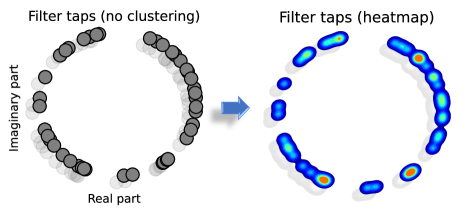
This cluster formation can be explained by the fact that the filter tap definition given by Eq. (1) represents a rotating vector with constant amplitude and varying phase as tap index varies. Therefore, a multiplication by a filter tap can be seen as simply a phase shift of the input sample with a constant scaling factor at the end. As the absolute phase increases for different values of , many phases will be repeated (because the even symmetry due to the term) or have values very close to each other on the complex plane circle because the values greater than just represent multiple rounds on the complex circle.
In this paper, we show how the analysis of the clusters of phase shifts makes it possible to reduce the complexity of the time domain equalizer through the utilization of factorization of the finite impulse response (FIR) filtering process, executing first the sums of the samples associated with filter taps that are grouped and then multiplying the sum result by the filter tap that represents the group, which we call the clustered filter tap.
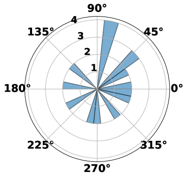
To investigate further this overlapping, in Fig. 2 we plot circular histograms to statistically analyze the angle distribution for equalizing filters in two different scenarios. The filter size utilized was 60% of the maximum number of taps in Eq. (2), which gives a considerable reduction in the filter size with minimal penalties [23].
| 80km, 27 taps | 8000km, 2647 taps |
|---|---|
 |
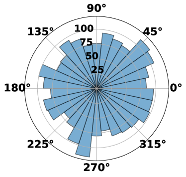 |
Fig. 2 reveals two distinct patterns: for short-range distances, we see a cluster formation (also illustrated in Fig 1), and for long-haul distances, the angle distribution is more spread but with some more occupied clusters (e.g., near 45° and 270°).
To assess how concentrated in clusters or evenly spread the filter taps are for different fiber lengths, let us introduce a simple metric ,
| (4) |
which is the difference between the number of taps in the most () and lowest () populated bins divided by the mean quantity of taps per bin , which is the total number of taps divided by the total number of bins. In an ideal uniform distribution, all the bins should be populated equally, therefore and . However, if the difference is bigger in comparison to , it means that at least one bin or more contains a higher concentration of taps than the others.
Looking at Fig. 3, one can conclude that for shorter distances, the distribution has one or more points of concentration (clusters), while as the distance increases, the angle distribution becomes more uniform and values decrease.
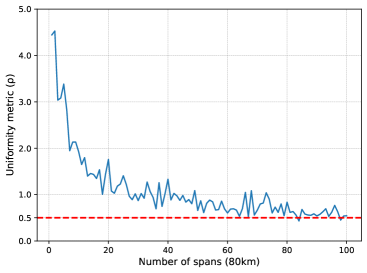
Taking as a reference, we can conclude that even for higher distances, which have a more uniform distribution, there is at least one cluster in the distribution. However, for these distances the concentration points are not so prominent. This result interpretation is in line with plots of Fig. 2.
II-B Complexity reduction by cluster analysis
Looking at the time domain convolution equation,
| (5) |
where is the filter size, we observe that the filter taps are directly multiplied by the input samples to produce the output samples . Thus, if some filter taps are grouped in clusters, each cluster can be represented by a single tap. This approximation can help decrease the complexity by using the distributive property of multiplication: we can first sum all the input samples associated with the grouped filter taps and then multiply this summed result by the tap representing the cluster. A similar use of this distributive property was employed to utilize the even symmetry of the transfer function [24, 9] and uniform quantization [9, 10], although none of those works harnessed the geometrical interpretation exploited here.
In this subsection, we explain and calculate the computational complexity, in terms of real multiplications per recovered symbol, of the resulting clustered filter obtained by considering the accumulation of angles in the complex plane, which we call complex-value (CV) clustering.
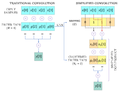
The FIR filtering by using Eq. (5) can simplified by CV clustering and expressed as a simplified convolution:
| (6) |
in which is the output sample index, represents the clustered filter taps to be multiplied by , which represents the summation of input samples that for each are associated with the same cluster of filter taps, and is the total number of complex value clusters.
The index of the input samples that must be summed before the multiplication by a specific clustered filter tap can be defined by a set in which is the cluster’s index varying from to . Therefore, the summation of associated input samples can be represented by:
| (7) |
These sets play the same role as the routing block described in Ref. [9].
Defining the complexity () as the number of real multiplications per recovered sample and noting that each complex multiplication is made up of 4 real multiplications, this strategy leads to the expression for the complex clustering complexity: .
|
|
|||
|
|
As we aim to demonstrate that, in hardware design, memory usage plays a significant role in both area usage and power consumption, we calculate here the minimum quantity of different memory positions needed to obtain the previously summed values (that we will also refer as pre-summed values). To calculate this, we observe that for each multiplication by in Eq. (6), the real and imaginary values of must be calculated previously and saved in memory, which means that memory positions are necessary to store .
III Methodology
In this work, we compare two variations of our approach with the state-of-the-art FDE. To find the clusters of filter taps in the complex plane, both TDCE variations use the unsupervised KNN algorithm [25], which has been successful in clustering and reducing equalization complexity in other scenarios [19, 20, 21]. One variation, TDCE GD, employs supervised learning with the Gradient Descent algorithm (GD) to further optimize the clusters to decrease the approximation errors caused by the clustering. The second variation, TDCE KNN, does not use supervised learning. The methodology for both approaches will be explained individually, considering that TDCE KNN methodology also applies to TDCE GD, with the latter including additional fine-tuning.
III-A TDCE KNN. Methodology
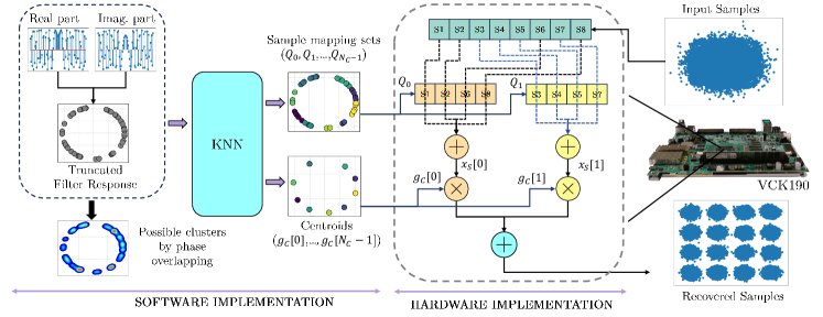
The clustering process is depicted on the left side of Fig. 5, showing the software implementation part. This involves using prior knowledge of variables , , , and to calculate the truncated filter response via Eq. (1). Subsequently, the KNN algorithm identifies the mapping sets and centroids for the clustered filter taps . The right side of Fig. 5 illustrates the hardware implementation of clustered filtering. This involves routing the input samples to the correct group based on the sample mappings , performing the summation of the samples in the same group to obtain , and at the end, multiplying the pre-summed values with clustered filter taps , and summing the outputs to get the recovered the symbol.
Our objective is to reach a in the final TDCE and FDE filters, corresponding to the error-free pre-FEC threshold with 7% overhead[26]. However, overall performance is compromised due to the inherent approximations in the clustering process. Therefore, we conducted an evaluation of the truncated filter response, Eq. (1), across various filter sizes, ranging from given by Eq. (2), to the minimum size that guarantees a BER below , as depicted in Fig. 4(a). Although this performance is better than our goal, the clustering process will decrease it. Following this, we evaluated the impact of different cluster quantities for each TDCE variation to determine the minimum number of clusters, ensuring a as shown in Fig. 4(b) for TDCE KNN. A similar approach, explained in detail in the sub-section III-C, is used for a fair comparison with the minimum complexity FDE.
To assess the filter performances, we utilized data obtained from numerical modeling of a single-channel, 32 GBaud, 16-QAM dual-polarization transmission at the optimal launch power across standard single-mode fiber (SSMF). The propagation dynamic was simulated employing the Manakov equation and the split-step Fourier method [27]. The SSMF parameters used were: dispersion ps/(nmkm), nonlinearity coefficient (Wkm)-1, and attenuation dB/km. Additionally, erbium-doped fiber amplifiers (with a noise figure of 4.5 dB) were included after each fiber span of 80 km. The number of spans ranged from 1 to 8, and all filters operated at 2 samples per symbol.
III-B TDCE GD (fine-tuning). Methodology
The taps clusterization process presented utilizes KNN, which is an unsupervised learning method that introduces an approximation error, creating a trade-off between complexity and performance (Fig. 4b). This section presents the application of supervised learning through the GD algorithm to decrease this approximation error and achieve lower complexity.
To optimize the process, we utilized the clustering scheme shown in Fig. 5(left), identical to the one used for TDCE KNN, to produce clustered filter taps (centroids). We subsequently developed a convolutional neural network (CNN) in software, initializing it with these centroids. The CNN was trained using pre-summed values , calculated by Eq. (7) from samples that simulated propagation through SSMF, as features (input data). The labels (desired predictions) were derived from the samples prior to optical fiber propagation simulation.
The total experimental dataset used consisted of symbols for the training dataset and independently generated symbols for the testing phase, each with different random seeds. Each training epoch utilized randomly selected samples from the training dataset, ADAM optimizer with a learning rate of , 400 training epochs. A training “stop condition” of 50 epochs with no BER improvement was also implemented. The testing phase utilized the first samples from the testing dataset, as this quantity was enough for the model to continuously learn until the early stop condition was reached.
An interesting finding of this strategy is that the centroids optimized by supervised learning became outside of the circle as an effect of correcting the approximation error introduced by the clustering process, as shown in Fig. 4(f). As a result, this fine-tuning reduced the number of clusters needed to reach the pre-FEC threshold considered in this paper, leading to a lower complexity filter with complexity savings of 33.3%, 20% and 20% for 1, 2, and 4 spans, respectively, in comparison to TDCE KNN and, 30.3%, 14.3%, 22.4% in comparison to FDE, as illustrated in Fig. 4(g).
III-C FDE. Methodology
We aim to benchmark our solution against the simplest FDE available to ensure a fair comparison. We assessed the performance versus filter size as shown in Fig. 4(a) for the time-domain FIR filtering, identifying the minimum filter size necessary to satisfy the condition . Then, we determined the FFT size () that minimizes the complexity of the FDE, :
| (8) |
where represents the FFT size (block size), denotes the filter size, and is a constant equal to when using the Radix-2 architecture with FFT sizes that are powers of 2, or when using the Radix-4 architecture with FFT sizes that are powers of 4. We utilized the overlap-save method[28] to segment the input signal into blocks before applying the FDE. Therefore, the denominator of Eq. (8) represents the total number of samples not corrupted by the overlap-save method. This optimization process of finding the optimization process is illustrated in the plot of Fig. 4(c).
By using the methodology described in this section and in the previous ones, the filter parameters in our approach were defined as described in Table I.
| N | MTDCE | MFDE | NC(KNN) | NC(GD) | NFFT | |
|---|---|---|---|---|---|---|
| 1 span | 45 | 31 | 29 | 9 | 6 | 256 |
| 2 spans | 89 | 53 | 55 | 10 | 8 | 256 |
| 4 spans | 177 | 97 | 103 | 10 | 8 | 1024 |
| 8 spans | 353 | 189 | 201 | 12 | 12 | 4096 |
In that Table is the maximum filter size as defined by Eq. (2), is the filter size to achieve before clustering for both TDCE variations, is the filter size for FDE, and are the number of complex clusters for the TDCE KNN and TDCE GD respectively and is the FFT size used for FDE.
Although the pre-FEC threshold used to define the filter size for FDE was higher than the one for TDCE, it required slightly more taps () than the TDCE () in some cases, as shown in Table I. As the difference in the number of filter taps was 6.3% in the worst case (8 spans), we considered it negligible.
Having established the optimal number of clusters and FFT sizes, we proceed to calculate the complexity; the respective dependencies are given in Fig. 4(g) for the FDE and two TDCE variants. Notably, employing a time-domain approach allows us to attain a complexity level comparable to that of the FDE as measured in real multiplications per recovered symbol.
IV FPGA Implementation
IV-A Simplified Convolution
As the index of the filter taps overlapped at a specific angle is not consecutive, it is crucial to route the input samples correctly to the appropriate pre-summed array memory for the accumulation expressed in Eq. (7). This routing presents a significant challenge similar to the routing challenge mentioned in Ref. [9] as one of the further optimizations required in that approach. Further on, we explain the implementation of this routing block in detail.
The sample routing of our implementation is inspired by the ideas presented in Ref. [29]. Unlike the multiple sets described in Eq. (7), we use a single set, , as shown in Fig. 6. This set contains pointers for each filter tap position, indicating where each input sample should be accumulated in . This method enables sequential input sample reading and simultaneous routing using .
Fig. 6(left) illustrates a hypothetical output calculation for , treating convolution as the dot-product of a reversed sliding filter with taps over input samples. As detailed earlier and shown in Fig. 6, the KNN-based clustering process generates centroids for clustered filter taps ( clusters) and sample mapping (). This mapping, implemented as sequential memory, directs each input sample to a pre-summed set . This routing allows a simplified dot-product between and , as depicted in Fig. 6(right), leveraging the distributive property of multiplication.
IV-B Parallelization
The parallelization of TDCE is a novel aspect of our research. To explain this process, we expand on the simplified convolution shown in Fig. 6. As the simplified dot-product is simple and has a straightforward implementation, we focus on the summation process that involves issues like routing and parallel memory access. The pseudo-code in Algorithm 1 illustrates the steps to obtain , similar to the method in Ref. [29].
A possible strategy to boost computation speed is to fully unroll the loop in Algorithm 1 and execute all iterations in parallel. This requires reading positions of and accessing input sample positions simultaneously for accurate accumulation into . While this increases computational speed, it significantly increases hardware resource demands due to parallel random memory access and numerous sum operations. To efficiently use FPGA resources, we compute sequential output samples simultaneously rather than parallelizing each output sample. This optimization leverages the interpretation of time-domain convolution as a series of dot-products, detailed in Fig. 8.
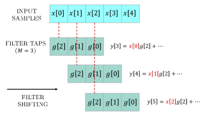
Fig. 8 illustrates convolution as a series of dot-products between sliding reversed filter taps and input samples, highlighting that the same filter tap multiplies consecutive input samples for successive outputs. Each filter tap in the original filter belongs to a cluster in the clustered filter, and each input sample must be routed to its corresponding clustered filter tap, as shown in Fig. 6. Since consecutive input samples are multiplied by the same filter tap across consecutive outputs, all input samples must be mapped to the same cluster. To utilize this property, we developed Algorithm 2.
Algorithm 2 leverages the property from Fig. 8, where the cluster index is read from once and used for all the innermost loop iterations. This property enables sequential reading of the input sample array . Since each output sample requires its own set, is now a bidimensional array in the algorithm. Additionally, the innermost loop is fully parallelizable, reducing the total number of iterations for the complete algorithm to . This significantly enhances throughput, making the total time period to perform the algorithm independent of .
IV-C TDCE Hardware Implementation Architecture
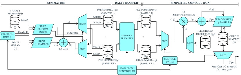
The hardware implementation of the TDCE is summarized in Fig. 7. To achieve high throughput, the architecture leverages the fact that the structure producing the pre-summed array is idle during the simplified dot-product stage, as shown in Fig. 6(right). This allows this structure to start processing the next samples while the simplified convolution of the previous ones is still ongoing. The Dataflow Controller block manages this process by controlling the Control Unit blocks for summation and simplified convolution.
In the summation structure, the sample mapping () is stored in a register and read sequentially for each filter tap (). Control Unit 1, enabled by the Dataflow Controller, enables the parallel reading of samples and one mapping simultaneously, times. This approach minimizes random access, as explained in Section IV-B. By pipelining this structure, we can organize the loop tasks—reading input, reading cluster index, reading memory banks, accumulation, and updating memory banks—to start a new iteration loop every clock cycle.
Controlled by the Dataflow Controller, the Memory Transfer block performs a bulk transfer of data from the summation memory banks (left) to secondary memory banks (right). This frees up the summation memory banks to process the next samples. Consequently, the structure can process new input samples before the simplified dot-product is finished.
After the Summation process is completed, the Simplified Dot-Product is executed. The number of multiplications in the Simplified Dot-Product is significantly less than the number of additions in the Summation, allowing multiplications to be performed at a lower rate, thus saving multipliers. For input samples, we define the number of parallel samples to be multiplied such that is a multiple of . This strategy ensures that the Simplified Dot-Product takes a similar amount of time as the summation process, enabling both operations to overlap. Control Unit 2 enables the reading of blocks of size to be multiplied by the same clustered filter tap. The resulting samples are accumulated in an output memory, which, at the end of the process, contains the output equalized samples. This multiply-and-accumulate (MAC) process is done for each cluster, resulting in iterations. Each iteration consists of internal iterations to perform MAC operations for all samples. Due to the overlapped execution, the system’s throughput (TH) is given by:
| (9) |
where is an empirical constant defined by the dataflow overlapping, and M is the filter size.
IV-D FDE Hardware Implementation Architecture
The FDE is used for comparison in this work because it is the common state-of-the-art reference in previous studies [9, 8, 11]. It offers the lowest complexity (calculated by Eq. (8)) compared to time-domain FIR filters [24], a higher degree of parallelization and stability compared to IIR filters [24], and is preferred for ASIC implementations [16, 17]. The FDE is based on the FFT algorithm, which includes a forward FFT to transform the input signal block, multiplication in the frequency domain (FD) between the FD representations of the input signal and transfer function, followed by an IFFT operation, and discarding of corrupted samples by the circular convolution (Fig. 9 right) [30]. To implement FDE, a method for block division and subsequent filtering of the signal is required, with Overlap-Add (OA) and Overlap-Save (OS) being well-known options [28]. In this work, we use OS for our FDE implementation. However, hardware resources for block division were not considered, as we aim to compare only the mathematical operations of the filters.
To compare our solution with the state-of-the-art FDE, we used the FFT HLS Library [31] developed and optimized by AMD® for the FFT/IFFT blocks. This ensures an unbiased and fair comparison since it was developed independently of our research. This FFT module offers different architecture options, allowing users to choose the suitable trade-off between hardware resources and throughput (Fig. 9 left). In this work, we used the Radix 4 Burst/IO architecture for medium output throughput, as the high throughput realization of TDCE will be addressed in future studies.
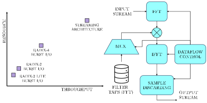
The Radix 4 Burst/IO architecture is not pipelined and has a latency before outputting data for each transformation cycle. To mitigate this and achieve higher throughput for FDE, we applied a dataflow HLS directive to implement the structure shown in Fig. 9(right). This allows the FFT block’s data output to overlap with the FD multiplication and the IFFT’s subsequent latency. Using dataflow, the throughput for FDE can be estimated by:
| (10) |
in which is the latency for the FFT size used and is an empirical constant determined by the dataflow structure.
As the IP block from AMD® does not allow a controllable parallelization, for simplicity, the throughput of TDCE was adjusted accordingly to match the same FDE throughput by adjusting the parameter in Eq. (9).
IV-E Implementation Parameters and Methodology
In all subsequent analyses, we implemented both filters on a VCK190 FPGA by simulations in the AMD® Vitis IDE at a clock frequency of 250 MHz. Both filters applied identical quantization to the taps and signals to ensure a fair comparison. A total of 16 bits, with 5 for integer bits, were used for the TDCE, and a total of 16 bits, with 1 integer bit, were used for the FDE to meet the threshold. All the filters were implemented aiming a BER, and the achieved BER values for the parameters used are described in Table II.
| BERGD | BERKNN | BERFDE | |
|---|---|---|---|
| 1 span | |||
| 2 spans | |||
| 4 spans | |||
| 8 spans |
Additionally, all the TDCE implementations were designed to achieve the same throughput as FDE with a maximum error difference of less than 7%, balancing the trade-off between digital filter throughput and hardware resources. The parameters of the parallelization of TDCE approaches and the achieved throughput are summarized in Table III.
| LGD | LKNN | LP-GD | LP-KNN | THGD | THTDCE | THFDE | |
|---|---|---|---|---|---|---|---|
| 1 span | 8 | 10 | 2 | 2 | |||
| 2 spans | 10 | 12 | 2 | 2 | |||
| 4 spans | 18 | 20 | 2 | 2 | |||
| 8 spans | 36 | 36 | 2 | 2 |
The equalizers were implemented using C++ in Vitis HLS 2023.2, which translates the code to HDL and generates RTL. The RTL was then implemented in Vivado 2023.2 using the default routing strategy. Energy consumption was assessed with the Power Estimator tool in Vivado. Power consumption in digital circuits comprises static and dynamic power. We focused on the dynamic power of the filters, excluding static power, which is associated with all inner circuits regardless of their usage in FPGA implementations. Additionally, dynamic power is the dominant factor in power consumption for ASIC implementations [17].
IV-F Memory Impact
Memory requirements and their hardware implementation are often not discussed in the evaluation of proposed algorithms for CDC [8, 9, 10]. Here, we demonstrate that this is an important issue to be considered that can impact the hardware implementation results noticeably.
To analyze the impact of memory implementation, TDCE KNN and FDE were implemented on FPGA, following the steps in Section III for a fiber length of 4 spans (320 km). Results are shown in Fig. 11. The implementation used two types of memory for the bank memories of (Fig. 7) in TDCE and inside the FFT/IFFT blocks of FDE (Fig. 9 right). Table I shows that for TDCE, was used to achieve 81.3Mb/s, while for FDE, was used to achieve 79.5Mb/s.
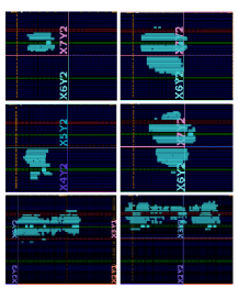
Fig. 11(a,b) illustrates the impact of using BRAMs for TDCE memory implementation. With parallel samples processed, the total number of BRAMs is 40, as memory banks are used before and after the Memory Transfer block (Fig. 7). This configuration reduces the quantities of LUTs and FFs compared to using LUTRAM, while the number of DSPs remains unaffected. However, dynamic power is higher when using BRAMs.
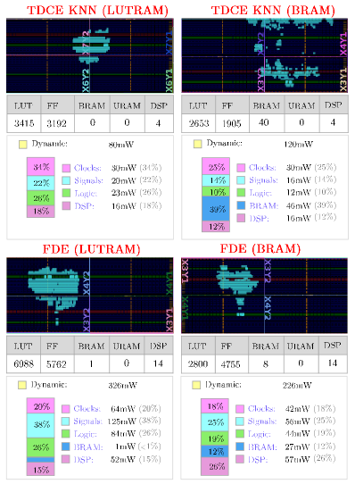
Also, because in this FPGA model, the BRAMs are physically disposed of in columns [32], the chip area usage is bigger, and a bigger effort must be made by the implementation tools to route the design achieving the right timing constraints. Knowing that for this fiber length, the amount of clusters is 10 (Table I) and looking at Fig. 7, we conclude that each memory bank has only 10 positions, each position storing a complex number with real and imaginary parts containing 16 bits each, what gives a total of 320 bits. However, each BRAM is able to store 36 kbits [32], which draws us to the conclusion that for this kind of memory, the usage efficiency is very low. This can be explained by the fact that each BRAM has only two ports [32], and to permit the Memory Transfer block (Fig. 7) to copy the data from the bank memories with high speed, a larger number of memories must be used to allow simultaneous access.
In this FPGA model, BRAMs are physically disposed of in columns [32], increasing chip area usage, as shown in Fig. 11(a,b). This spreading of the chip area requires greater effort by implementation tools to meet timing constraints during routing, potentially causing timing issues in higher throughput cases that require larger areas. For the given fiber length, TDCE uses 10 clusters (Table I), resulting in each memory bank having only 10 positions, as shown in Fig. 7. Each position stores one complex number with 16-bit real and imaginary parts, totaling 320 bits per bank. However, each BRAM can store 36 kbits [32], resulting in very low usage efficiency. This inefficiency is due to each BRAM having only two ports [32], necessitating a larger number of memories to allow high-speed data transfer by the Memory Transfer block (Fig. 7) and simultaneous access.
Analyzing Fig. 11(c,d), we see that for the FDE, unlike the TDCE, dynamic power, and area usage are higher when using LUTRAM memory while the number of DSPs is not affected. As expected, the number of LUTs and FFs is greater when LUTRAM is used.
From the above analysis, we conclude that for FPGA implementation, the optimal choice in terms of chip area usage, routing, and power efficiency is to use LUTRAMs for memory banks in TDCE. In contrast, for the FDE, BRAMs are the better choice for the FFT/IFFT blocks. These memory implementations will be used in the following discussions.
IV-G Results for Different Distances
From Fig. 10(a), we observe that the chip areas required by the GD and KNN approaches are quite similar due to their use of similar amounts of resources. Additionally, for low dispersion scenarios like 1 fiber span, the area required for the TDCE designs is smaller than that required for the FDE. However, for higher dispersion scenarios, like 8 spans, the area required is similar for all designs.
Fig. 10(b) shows that, due to the memory implementation choices, both TDCE filters do not use BRAMs, in contrast to the FDE, which uses 8. However, the LUT quantities used by TDCE approaches are higher than those for the FDE, as explained in subsection IV-F. In addition, despite having the highest complexity in this work according to Fig. 4(f), TDCE KNN used about one-third of the multipliers required by FDE and the same amount of multipliers as TDCE GD. This is because the multiplications for TDCE are done after the summation with overlapping between tasks (Fig. 7).
To illustrate how our parallelization can save multipliers, consider the TDCE KNN for 4 spans with , , and (Table I). The summation process takes about clock cycles, independent of (subsection IV-B), plus around clock cycles to transfer data to secondary memory banks, totaling approximately clock cycles, which can be rounded to 110 due to extra dataflow cycles. Each output sample requires multiplications, totaling 200 multiplications that can be completed in the 110 clock cycles due to task overlapping. Thus, the multiplications can be performed with a smaller degree of parallelism (), allowing for two complex multiplications per clock cycle (). Since each complex multiplication has two real multiplications, this implementation uses only 4 multipliers compared to the 14 used by FDE.
Despite having lower complexity, the GD implementation required the same number of multipliers as the KNN due to needing clusters. This requires fewer parallel samples, , totaling complex multiplications. These cannot be performed sequentially in approximately clock cycles (TDCE GD), necessitating the same degree of parallelism as the KNN, with 2 complex multiplications per clock.
Regarding energy efficiency, Fig. 10(c) shows that TDCE approaches have similar power consumption. This similarity is due to the similar quantities of required hardware resources and the same algorithm implementation. Both TDCE approaches consume less power than FDE, with significant energy savings in DSP and BRAM usage. This can be attributed to the fewer multipliers required by TDCE designs and the use of LUTs and FFs instead of BRAMs. Additionally, energy savings in Signals are notable, thanks to the simpler TDCE algorithm, which avoids the interconnected structures of the FFT algorithm that uses deeply interconnected ”butterflies” for operations [13]. These power-distributed savings result in superior overall energy efficiency for TDCE approaches compared to FDE, as shown in Fig. 10(d), with an efficiency gain of up to 70.4%, even for the higher complexity TDCE KNN. This demonstrates that hardware implementation is as crucial as mathematical complexity in determining energy efficiency. Both TDCE designs exhibit very similar energy efficiency despite the GD approach being less complex. This is because the reduced number of required multiplications did not significantly reduce the number of multipliers due to the dataflow structure.
V Conclusion
We presented a geometrical interpretation of the CDC transfer function and explained the effect of filter taps overlapping. This overlapping generates clusters of filter taps, which we harnessed to decrease the theoretical complexity of time-domain FIR filtering. Our approach was further optimized using machine learning to reduce computational complexity. We implemented the proposed solution and state-of-the-art FDE on FPGA for different fiber lengths (from 80 km to 640 km SSMF) and examined energy efficiency using the nJ/bit metric. We quantified the impact of memory implementation on resource quantity, energy efficiency, chip area usage, and routability in FPGA realization. The developed TDCE technique demonstrated up to 71.4% savings in the number of multipliers, even for higher computational complexity cases in comparison to FDE. Furthermore, we showed that TDCE can be flexibly parallelized by leveraging the property that in linear convolution, the same filter tap multiplies consecutive input samples across consecutive output sample calculations.
In conclusion, for the considered fiber lengths, the proposed TDCE achieved up to 70.7% energy savings compared to the FDE, better chip area usage, a slightly higher usage of LUTs, and a lower usage of FFs, despite implementing memory without BRAMs.
VI Acknowledgments
The authors utilized ChatGPT 4 for Python, C++, and LaTeX coding support, as well as Grammarly and ChatGPT 4 for grammar correction and text clarification.
PF acknowledges AMD® for providing the VCK-190 board, Vivado License, and consultancy during the design of the algorithms. SKT acknowledges the EPSRC project TRANSNET (EP/R035342/1).
References
- [1] E. Agrell, M. Karlsson, A. Chraplyvy, D. J. Richardson, P. M. Krummrich, P. Winzer, K. Roberts, J. K. Fischer, S. J. Savory, B. J. Eggleton et al., “Roadmap of optical communications,” Journal of Optics, vol. 18, no. 6, p. 063002, 2016.
- [2] M. Radovic, A. Sgambelluri, F. Cugini, and N. Sambo, “Power-aware high-capacity elastic optical networks,” Journal of Optical Communications and Networking, vol. 16, no. 5, pp. B16–B25, 2024.
- [3] P. J. Freire, S. Srivallapanondh, B. Spinnler, A. Napoli, N. Costa, J. E. Prilepsky, and S. K. Turitsyn, “Low-complexity efficient neural network optical channel equalizers: training, inference, and hardware synthesis,” in 2023 European Conference on Optical Communication (ECOC). IET Digital Library, 2023, pp. 1–4.
- [4] P. Freire, E. Manuylovich, J. E. Prilepsky, and S. K. Turitsyn, “Artificial neural networks for photonic applications—from algorithms to implementation: tutorial,” Advances in Optics and Photonics, vol. 15, no. 3, pp. 739–834, 2023.
- [5] C. Minkenberg, R. Krishnaswamy, A. Zilkie, and D. Nelson, “Co‐packaged datacenter optics: Opportunities and challenges,” IET Optoelectronics, vol. 15, pp. 77–91, 03 2021.
- [6] R. Nagarajan, I. Lyubomirsky, and O. Agazzi, “Low power dsp-based transceivers for data center optical fiber communications (invited tutorial),” Journal of Lightwave Technology, vol. 39, no. 16, pp. 5221–5231, 2021.
- [7] M. Kuschnerov, T. Bex, and P. Kainzmaier, “Energy efficient digital signal processing,” in Optical Fiber Communication Conference. Optica Publishing Group, 2014, pp. Th3E–7.
- [8] A. Felipe and A. L. N. d. Souza, “Chirp-filtering for low-complexity chromatic dispersion compensation,” Journal of Lightwave Technology, vol. 38, no. 11, pp. 2954–2960, 2020.
- [9] C. S. Martins, F. P. Guiomar, S. B. Amado, R. M. Ferreira, S. Ziaie, A. Shahpari, A. L. Teixeira, and A. N. Pinto, “Distributive FIR-Based Chromatic Dispersion Equalization for Coherent Receivers,” Journal of Lightwave Technology, vol. 34, no. 21, pp. 5023–5032, 2016.
- [10] Z. Wu, S. Li, Z. Huang, F. Shen, and Y. Zhao, “Low-complexity chromatic dispersion equalization fir digital filter for coherent receiver,” Photonics, vol. 9, no. 4, 2022. [Online]. Available: https://www.mdpi.com/2304-6732/9/4/263
- [11] Z. Ji, R. Ji, M. Ding, X. Song, X. You, and C. Zhang, “Hardware implementation of chromatic dispersion compensation in finite fields,” in 2023 IEEE 15th International Conference on ASIC (ASICON), 2023, pp. 1–4.
- [12] T. Xu, G. Jacobsen, S. Popov, J. Li, E. Vanin, K. Wang, A. T. Friberg, and Y. Zhang, “Chromatic dispersion compensation in coherent transmission system using digital filters,” Opt. Express, vol. 18, no. 15, pp. 16 243–16 257, Jul 2010. [Online]. Available: https://opg.optica.org/oe/abstract.cfm?URI=oe-18-15-16243
- [13] J. W. Cooley and J. W. Tukey, “An algorithm for the machine calculation of complex fourier series,” Mathematics of computation, vol. 19, no. 90, pp. 297–301, 1965.
- [14] C. Bae and O. Gustafsson, “Finite word length analysis for fft-based chromatic dispersion compensation filters,” OSA Advanced Photonics Congress 2021, p. SpTh1D.3, 2021. [Online]. Available: https://opg.optica.org/abstract.cfm?URI=SPPCom-2021-SpTh1D.3
- [15] ——, “Fft-size implementation tradeoffs for chromatic dispersion compensation filters,” Advanced Photonics Congress 2023, p. SpTu3E.1, 2023. [Online]. Available: https://opg.optica.org/abstract.cfm?URI=SPPCom-2023-SpTu3E.1
- [16] H. Sun, M. Torbatian, M. Karimi, R. Maher, S. Thomson, M. Tehrani, Y. Gao, A. Kumpera, G. Soliman, and A. Kakkar, “800G DSP ASIC design using probabilistic shaping and digital sub-carrier multiplexing,” Journal of Lightwave Technology, 2020.
- [17] C. Fougstedt, O. Gustafsson, C. Bae, E. Börjeson, and P. Larsson-Edefors, “ASIC design exploration for DSP and FEC of 400-Gbit/s coherent data-center interconnect receivers,” in Optical Fiber Communication Conference. Optica Publishing Group, 2020, pp. Th2A–38.
- [18] A. Kovalev, O. Gustafsson, and M. Garrido, “Implementation approaches for 512-tap 60 GSa/s chromatic dispersion FIR filters,” in 2017 51st Asilomar Conference on Signals, Systems, and Computers. IEEE, 2017, pp. 1779–1783.
- [19] X. Huang, F. Xie, D. Tang, S. Liu, and Y. Qiao, “Low-complexity clustered polynomial nonlinear filter-based electrical dispersion pre-compensation scheme in im/dd transmission systems,” Optics Express, vol. 31, no. 20, pp. 32 529–32 542, Sep 2023. [Online]. Available: https://opg.optica.org/oe/abstract.cfm?URI=oe-31-20-32529
- [20] F. Xie, S. Liu, X. Huang, H. Cui, D. Tang, and Y. Qiao, “Low-complexity optimized detection with cluster assisting for c-band 64-gb/s ook transmission over 100-km ssmf,” Opt. Express, vol. 31, no. 12, pp. 18 888–18 897, Jun 2023. [Online]. Available: https://opg.optica.org/oe/abstract.cfm?URI=oe-31-12-18888
- [21] F. Xie, X. Huang, S. Liu, D. Tang, C. Bai, H. Xu, and Y. Qiao, “Deployment of ultrasmall-size cluster-assisting lookup tables in im/dd systems,” J. Lightwave Technol., vol. 42, no. 9, pp. 3118–3127, May 2024. [Online]. Available: https://opg.optica.org/jlt/abstract.cfm?URI=jlt-42-9-3118
- [22] M. G. Taylor, “Compact digital dispersion compensation algorithms,” in OFC/NFOEC 2008 - 2008 Conference on Optical Fiber Communication/National Fiber Optic Engineers Conference, 2008, pp. 1–3.
- [23] S. J. Savory, “Digital filters for coherent optical receivers,” Optics Express, vol. 16, no. 2, pp. 804–817, Jan 2008.
- [24] B. Spinnler, “Equalizer design and complexity for digital coherent receivers,” IEEE Journal of Selected Topics in Quantum Electronics, vol. 16, no. 5, pp. 1180–1192, 2010.
- [25] Z. Zhang, “Introduction to machine learning: k-nearest neighbors,” Annals of Translational Medicine, vol. 4, no. 11, 2016. [Online]. Available: https://atm.amegroups.org/article/view/10170
- [26] E. Agrell and M. Secondini, “Information-theoretic tools for optical communications engineers,” in 2018 IEEE Photonics Conference (IPC). IEEE, 2018, pp. 1–5.
- [27] G. P. Agrawal, Nonlinear Fiber Optics, 6th edt. Academic Press, 2019.
- [28] T. Xu, G. Jacobsen, S. Popov, M. Forzati, J. Mårtensson, M. Mussolin, J. Li, K. Wang, Y. Zhang, and A. T. Friberg, “Frequency-domain chromatic dispersion equalization using overlap-add methods in coherent optical system,” Journal of Optical Communications, vol. 32, no. 2, pp. 131–135, 2011. [Online]. Available: https://doi.org/10.1515/joc.2011.022
- [29] M. Samragh, M. Ghasemzadeh, and F. Koushanfar, “Customizing neural networks for efficient fpga implementation,” in 2017 IEEE 25th Annual International Symposium on Field-Programmable Custom Computing Machines (FCCM). IEEE, 2017, pp. 85–92.
- [30] T. Xu, G. Jacobsen, S. Popov, J. Li, E. Vanin, K. Wang, A. T. Friberg, and Y. Zhang, “Chromatic dispersion compensation in coherent transmission system using digital filters,” Opt. Express, vol. 18, no. 15, pp. 16 243–16 257, Jul 2010. [Online]. Available: https://opg.optica.org/oe/abstract.cfm?URI=oe-18-15-16243
- [31] Xilinx, “Fast fourier transform logicore ip product guide (pg109),” https://docs.amd.com/r/en-US/pg109-xfft, 2024, accessed: 2024-07-29.
- [32] ——, “Versal acap memory resources architecture manual (am007),” https://docs.amd.com/r/en-US/am007-versal-memory/Block-RAM-Introduction, 2024, accessed: 2024-07-29.