Programmable multifunctional integrated microwave photonic circuit on thin-film lithium niobate
Abstract
Microwave photonics, with its advanced high-frequency signal processing capabilities, is expected to play a crucial role in next-generation wireless communications and radar systems. The realization of highly integrated, high-performance, and multifunctional microwave photonic links will pave the way for its widespread deployment in practical applications, which is a significant challenge. Here, leveraging thin-film lithium niobate intensity modulator and programmable cascaded microring resonators, we demonstrate for the first time a tunable microwave photonic notch filter that simultaneously achieves high level of integration along with high dynamic range, high link gain, low noise figure, and ultra-high rejection ratio. Additionally, this programmable on-chip system is multifunctional, allowing for the dual-band notch filter and the suppression of the high-power interference signal. This work demonstrates the potential applications of the thin-film lithium niobate platform in the field of high-performance integrated microwave photonic filtering and signal processing, facilitating the advancement of microwave photonic system towards practical applications.
I Introduction
Traditional radio frequency (RF) filtering technologies are increasingly insufficient to meet the demands of future communication systems, which require large bandwidth, programmability, multifunctionality, and reductions in volume, weight, and power consumption akyildiz20206g . Integrated microwave photonic (MWP) filters exploit the inherent broadband and flexible tuning characteristics of photonic components, combined with existing photonic integration technologies, to forge a new path for RF signal processing yao2009microwave ; capmany2007microwave ; marpaung2013integrated ; marpaung2019integrated ; capmany2006tutorial ; liu2020integrated . In recent years, significant advancements have been made in integrated MWP circuits. However, these studies often struggle to simultaneously achieve high integration fandino2017monolithic , multifunctionality perez2017multipurpose ; perez2020multipurpose ; bogaerts2020programmable , and excellent RF metrics cox2006limits ; lim2009fiber ; liu2018link , which are critical for practical RF applications.
In MWP systems, electro-optic modulators are responsible for faithful RF-to-optical conversion, and nearly all challenges stem from the modulator. The widely demonstrated MWP filters based on silicon-on-insulator (SOI) rasras2009demonstration ; qiu2018continuously ; tao2023highly ; tao2021hybrid ; zhang2022ultralow ; yan2023wideband or silicon nitride roeloffzen2013silicon ; taddei2014fully ; marpaung2013si ; daulay2022ultrahigh ; liu2017all ; zhuang2015programmable microring resonators, as well as those utilizing the stimulated Brillouin scattering (SBS) effect in waveguides casas2015tunable ; marpaung2015low ; gertler2022narrowband ; garrett2023integrated ; botter2022guided ; gertler2020tunable ; ye2023brillouin , typically make use of commercial external lithium niobate modulators or compact SOI chip-based modulators for electro-optic conversion. The aforementioned approaches have limitations because commercial external lithium niobate modulators present challenges for high level of integration due to their large size, and the large half-wave voltage also limits link gain. Although silicon photonics technology has enabled the integration of modulation reed2010silicon ; xu2005micrometre ; li2018silicon and MWP functions on the same photonic chip with reduced footprint, the typically higher drive voltages required by silicon modulators present challenges for linearity and power handling, which are problems particularly for MWP applications.
Thin-film lithium niobate (TFLN), with its strong and linear electro-optic effect and low waveguide propagation loss zhang2017monolithic , represents an ideal platform for high-performance modulators wang2018integrated ; mercante2018thin ; wang2018nanophotonic ; rao2017compact ; he2019high ; zhang2021integrated ; xu2020high ; kharel2021breaking and other optical components zhu2021integrated ; boes2023lithium ; feng2024integrated . Therefore, TFLN is an ideal platform for fabricating integrated MWP circuits, as it provides excellent electro-optic performance and supports a variety of components, allowing the possibility of integrating everything in a single circuit snigirev2023ultrafast ; yu2023integrated . However, to date, there has yet to be a demonstration of integrating TFLN modulators and programmable optical structures on the same chip to achieve multifunctional MWP circuits.
In this work, we demonstrate for the first time a highly reconfigurable TFLN MWP circuit with three distinct functionalities in a compact footprint. By integrating an intensity modulator and cascaded programmable microring resonators on a single chip, we have achieved a tunable notch filter with high rejection ratio, enhanced the spurious free dynamic range (SFDR) by suppressing third-order intermodulation distortion (IMD3), and suppressed the high-power interference signals that are very close in frequency to the signal of interest.
The notch filter can be tuned over a frequency range of 20 GHz and can switch between single-band and dual-band operation while maintaining a rejection ratio beyond 60 dB. The linearization method suppresses IMD3 by 34 dB, increasing the SFDR of the notch filter to 110 dB in 1 Hz. Additionally, high-power interference signals that are very close in frequency to the signal of interest can be suppressed by 56 dB. Our demonstration illustrates the feasibility of achieving multifunctional and high-performance MWP circuits in a compact footprint, contributing to the application of integrated MWP technology in future communication systems.
II Results
Multifunctional microwave photonic circuit
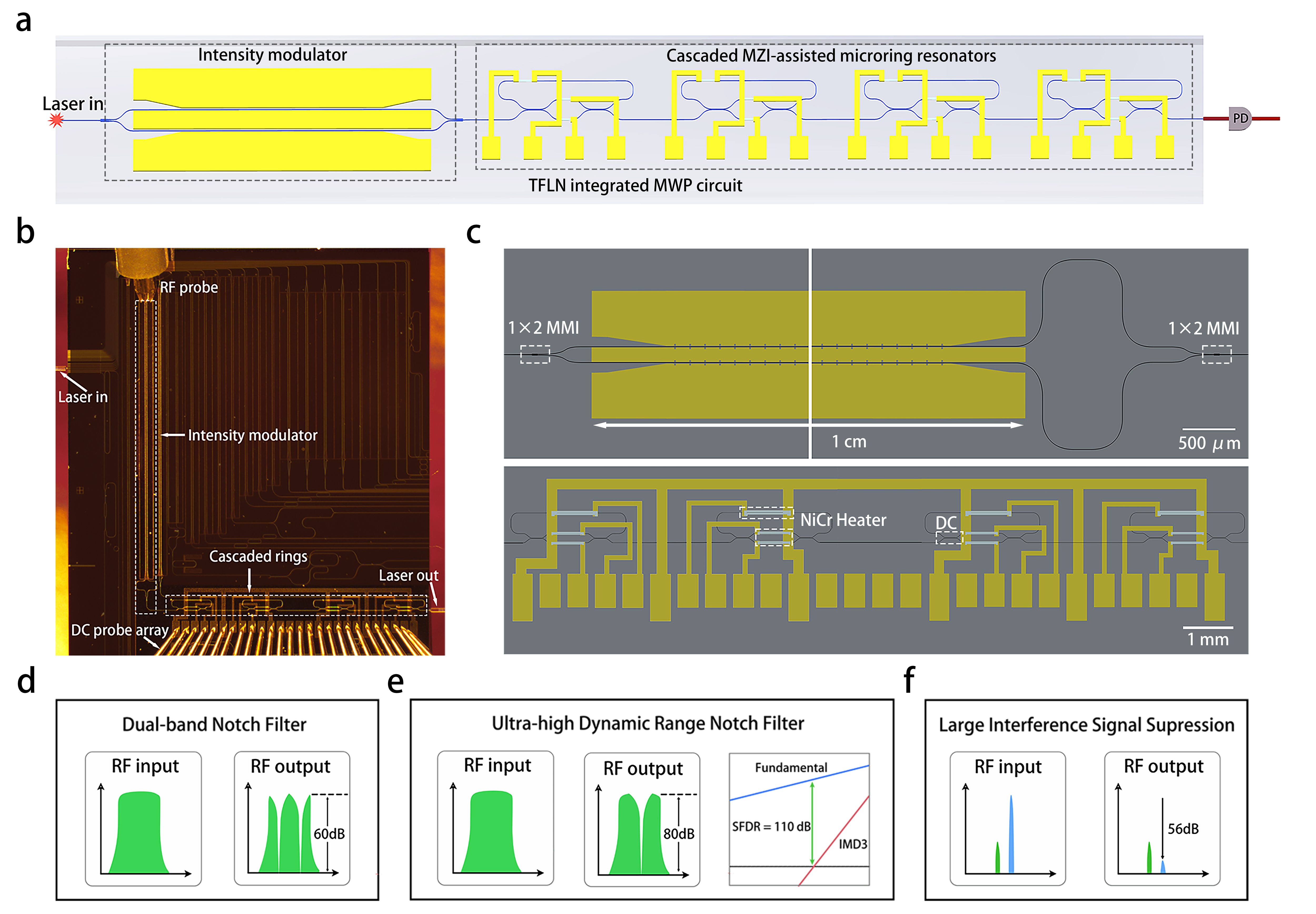
The structural diagram of the chip is shown in Fig.1a. It consists of a TFLN intensity modulator and four cascaded programmable microrings. The intensity modulator converts the RF signal into the optical domain, and the modulation sidebands are processed by Mach-Zehnder Interferometer (MZI)-assisted microrings, whose coupling coefficient and resonant wavelength can be adjusted via thermal phase shifters. This forms the basis of our multifunctional capability. Fig.1b shows a microscope image of the chip and the experimental setup. The chip employs edge coupling structure, with light coupled in and out via lensed fibers. The insertion loss is 14 dB, which can be reduced by designing a specialized taper structure he2019low .
We load the RF signal onto the modulator electrodes using a GSG structure RF probe and control the cascaded microrings with a 26-channel DC probe array. Fig.1c is a false-color optical image of the chip. The modulator electrode is 1 cm long and adopts a slot electrode structure, with a V of 3.5V at 5GHz. The characterization method for RF V is provided in Supplementary Information I. The coupling region of the microrings consists of a directional coupler and an MZI, with heaters (grey) on the MZI arms acting as phase shifters. By precisely controlling the voltage applied to the heaters, each microring can be set to a specific coupling state. Heaters in the racetrack region of the microrings are used to change the resonance positions. Detailed experimental results for the response of the cascaded microrings can be found in Supplementary Information II.
We have achieved three distinct functionalities based on this circuit. The first functionality is a dual-band notch filter that can simultaneously filter out any two unwanted signals with a rejection ratio of up to 60 dB, as shown in Fig.1d. The second functionality is an ultra-high dynamic range notch filter that improves the SFDR to 110 dB in 1 Hz while maintaining an 80 dB rejection ratio, as shown in Fig.1e. The third functionality can suppress high-power interference signal with frequency close to the signal of interest, as illustrated in Fig.1f.
Tunable notch filter
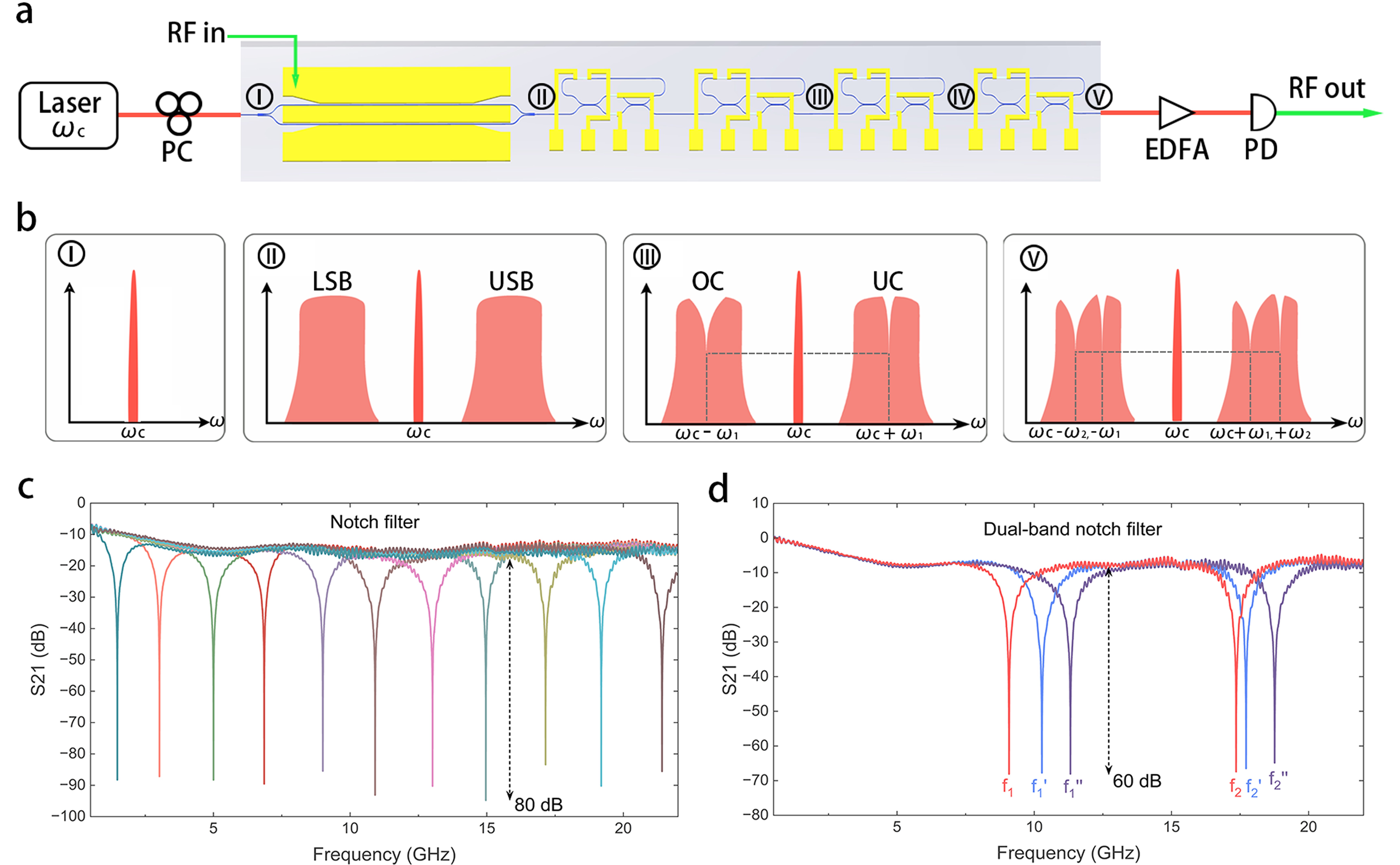
The schematic of the entire microwave photonic link setup is shown in Fig.2a. In this demonstration, we use a sweep signal generated by a vector network analyzer (VNA) as the RF input. Fig. 2b illustrates the spectra at different nodes. After the optical carrier passes through the intensity modulator, two in-phase modulation sidebands are generated, as shown at Node II. The spectrum after processing by the two microrings is depicted at Node III. It can be observed that the resonance positions of the two microrings are symmetric with respect to the optical carrier, and their suppression ratios are identical. The difference lies in the coupling states, with one microring in the undercoupled state with 0 phase shift and the other microring in the overcoupled state with phase shift. This meets the condition for destructive interference, leading to the ultra-high rejection ratio. Meanwhile, other parts of the modulation sidebands that are not processed by the microrings still add constructively, ensuring high link gain for the system.
Fig.2c presents the tunable notch filter response with the modulator operating at the quadrature point. The maximum link gain is -7 dB, with a suppression ratio of up to 80 dB and a 3-dB bandwidth of 1.3 GHz. This filter can be continuously tuned from 1.5 GHz to 21.5 GHz, as the tuning range is limited by the microrings’ Free Spectral Range (FSR) of 44 GHz. Additionally, when the modulator is set to operate at the null point and the other two microrings are turned on, the output spectrum is as shown at Node V. Based on the same working principle mentioned earlier, we achieved a tunable dual-band notch filter with a maximum link gain of 0 dB and a rejection ratio of up to 60 dB, as shown in Fig.2d.
In this experiment, the choice of bias point directly affects the link gain and noise figure due to the use of an intensity modulator for electro-optic conversionliu2018link . However, since we placed the Erbium-Doped Fiber Amplifier (EDFA) directly before the photodetector (PD), the low bias technique could not optimize the noise figure, and it remained stable around 35 dB regardless of the bias voltage changes. We employed a bias tee to control the bias point, and detailed analyses of link gain and noise figure at different bias voltages are provided in Supplementary Information III.
Linearization for high dynamic range
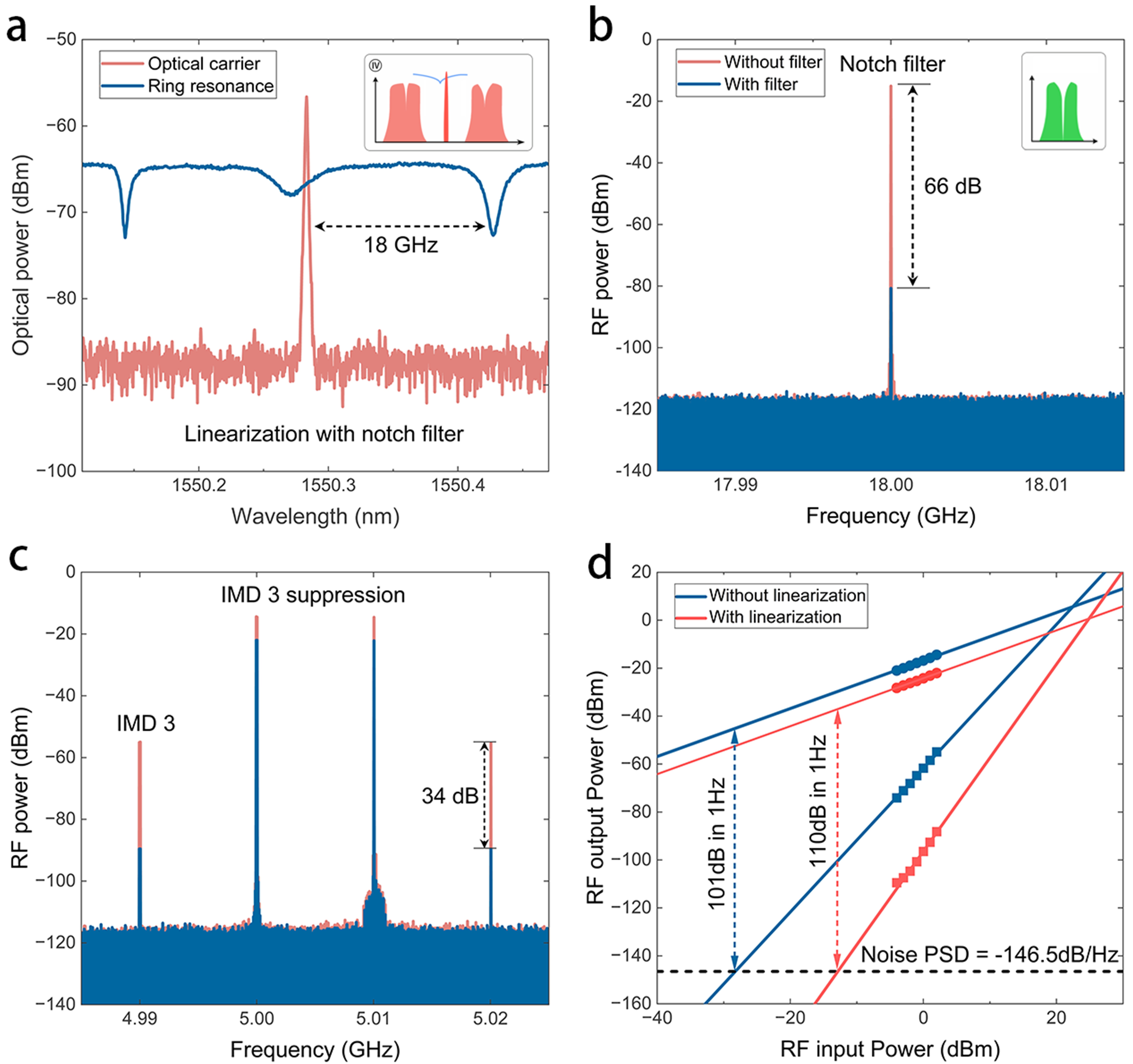
When two RF signals of different frequencies are input into the microwave photonic system, intermodulation distortion (IMD) occurs, limiting the system’s dynamic range. We utilize the response of microrings to shape the optical carrier, thereby suppressing the third-order intermodulation distortion (IMD3) and improving the spurious-free dynamic range (SFDR). The relative positions between the optical carrier and the microring resonance peaks when achieving the ultra-high dynamic range notch filter are shown in Fig.3a. This result was obtained from an optical spectrum analyzer (OSA), which corresponds to the spectrum at Node IV in Fig.2a.
The responses of overcoupled and undercoupled microrings with identical suppression ratios are symmetrically distributed around the optical carrier, enabling the filtering function. The filtering result is shown in Fig.3b, where the red curve represents the RF output without filtering and the blue curve represents the filtered RF output. Concurrently, a third overcoupled microring is employed to process the optical carrier. Under specific conditions, we successfully suppressed the IMD3. (see Supplementary Information IV)
In the linearization demonstration, we utilized a two-tone signal generated by two signal generators as input, with the modulator operating at the quadrature point. Fig.3c illustrates the RF output from the two-tone test. It can be seen that after linearization, IMD3 is suppressed by 34 dB. From Fig.3d, it is evident that with a noise power spectral density (PSD) of -146.5 dBm/Hz in the system, the SFDR was 101 dB in 1 Hz without linearization, and it improved to 110 dB in 1 Hz after linearization. Additionally, it can be observed that after linearization, the slope of the intermodulation distortion terms has changed due to the severe suppression of IMD3, as previously insignificant fifth-order intermodulation signals start to affect the output results.
| Year |
|
|
|
|
|
|
|
|
||||||||||||||||
| 2020gertler2020tunable | Si | Passive | SBS | 1 | No | -17.3 | 56.7 | 93.5 | ||||||||||||||||
| 2021tao2021hybrid | Si | MD, Passive, PD | MRR | 2 | No | -28.2 | 51.2 | 99.7 | ||||||||||||||||
| 2022daulay2022ultrahigh | Si3N4 | Passive | DI-MRR | 6 | SFDR, NF | 10 | 15 | 116 | ||||||||||||||||
| 2022gertler2022narrowband | Si | Passive | SBS | 1 | No | -3.6 | 52.5 | 93.6 | ||||||||||||||||
| 2023tao2023highly | Si | MD, Passive, PD | MRR | 2 | No | -27 | 47 | 92.3 | ||||||||||||||||
| 2023garrett2023integrated | Si+As2S3 | MD, Passive | SBS | 2 | No | -35 | 57.5 | 80 | ||||||||||||||||
| This work | TFLN | MD, Passive | MRRs | 3 | SFDR | -7.2 | 34.7 | 110 | ||||||||||||||||
|
||||||||||||||||||||||||
Large interference signal suppression
In practical applications, the RF receiving front-end may encounter interference from high-power RF signals. When the frequency of the signal of interest and the interfering signal are very close, a filter with ultra-high resolution is needed to eliminate the interference. However, achieving extremely high-resolution MWP filters is a significant challenge. Here, we propose a method to suppress high-power interference signals. Fig.4a presents the experimental setup for demonstrating large interference signal suppression.
Fig.4b shows the RF and optical spectrum at different nodes. When a high-power RF signal is input, high-order modulation sidebands, as shown at node II, are generated. We utilize the response of the microrings to process these high-order sidebands, as illustrated by the spectrum at Node III. Figure 4c shows the actual optical spectrum corresponding to the animated spectrum at Node III. By precisely controlling the microring for shaping higher-order sidebands, the high-power interference signal can be suppressed under specific conditions (see Supplementary Information V). The low-power signal of interest remains unaffected because it does not generate high-order modulation sidebands.
In this demonstration, the modulator operates at the quadrature point, with the input power of the interference signal set at 23 dBm and the input power of the signal of interest at -24 dBm. The frequency spacing between the two signals is 5 MHz, an exceptionally narrow spacing that nearly no existing MWP circuits are capable of discriminating. The RF output without suppression is shown in Fig.4c, and the RF output after suppression is shown in Fig.4d. It can be observed that only the high-power signal is suppressed, with a suppression ratio of 56 dB.
III Discussion
Table I summarizes the performance of state-of-the-art integrated MWP circuits. In the past three years, research on MWP circuits based on SOI platforms has successfully integrated modulators with microrings tao2021hybrid ; tao2023highly or SBS spiral lines garrett2023integrated . However, these works have neglected improvements in RF performance, with system dynamic ranges often below 100 dB Hz2/3. Additionally, the relatively low electro-optic conversion efficiency of SOI modulators limits system link gain and noise figure. Although our previous research on the Si3N4 platform achieved improvements in RF performance and multifunctionality daulay2022ultrahigh , the demonstration still relied on off-chip modulators, and the integration level remains to be enhanced. In contrast, this work based on the TFLN platform combines miniaturization with high performance.
At present, in our demonstrations of all functionalities, we placed the EDFA directly before the PD. This configuration allows us to achieve maximum link gain when the modulator operates near the null point. However, to implement the linearization and large interference signal suppression, the modulator needs to operate at the quadrature point because the intensity relationship between the carrier and the sidebands is well-defined under this condition. This is a necessary condition for the equations presented in the Supplementary Information IV and V to have a definite solution, though it sacrifices some link gain.
Currently, our structure comprises only four cascaded microrings, limiting our ability to shape the optical carrier for linearization while implementing the dual-band notch filter. In future designs, we plan to increase the number of programmable microrings, enabling the simultaneous realization of multiple functionalities. To achieve high link gain, we currently rely on an external EDFA, which adds to the system’s size, weight, and power consumption. Recent advances in low-noise erbium-doped waveguide amplifiers liu2022photonic ; bao2024erbium could facilitate on-chip optical amplification, enhancing system integration.
In summary, we have designed and fabricated a programmable MWP circuit based on TFLN intensity modulator and cascaded microrings. Our experimental demonstrations highlight its multifunctionality, including high link gain, ultra-high dynamic range, ultra-high rejection ratio notch filter, as well as dual-band notch filter and suppression of large interference signals. These advancements represent a significant breakthrough for the application of microwave photonic technology in real-world communication and radar systems.
IV Methods
Device fabrication
The MWP circuit is fabricated from commercially available x-cut lithium niobate on insulator (LNOI) wafer (NANOLN), consisting of a 500 nm thick LN thin film, a 4.7 m thick buried SiO2 layer, and a 500 m thick silicon substrate. Firstly, SiO2 is deposited on the surface of a 4-inch LNOI wafer as an etching hard mask using plasma-enhanced chemical vapor deposition (PECVD). Various functional devices are patterned on the entire wafer using an ASML UV Stepper lithography system die-by-die with a resolution of 500 nm. Next, the exposed resist patterns are transferred first to the SiO2 layer using a standard fluorine-based dry etching process, and then to the LN device layer using an optimized Ar+ based inductively coupled plasma (ICP) reactive-ion etching process. The etching depth of the LN layer is 250 nm, leaving a 250 nm-thick slab. After the removal of the residual SiO2 mask and redeposition, an annealing process is carried out. Following the deposition of the SiO2 cladding using PECVD, the microwave electrodes, heater, and wires/pads are fabricated through the second, third, and fourth lithography and lift-off processes, respectively.
Details of experiments
We use a laser (Teraxion) with relative-intensity noise below -160 dBc/Hz as the optical carrier. After passing through a polarization controller, polarization beam splitter, and polarization rotator, 16.8 dBm of TE mode light is coupled into the TFLN chip. In the tunable filtering experiment, a sweep signal generated by VNA (Keysight 5007A) drives the intensity modulator. The optical signal output from the chip is amplified by a low-noise EDFA (Amonics) and then sent to a PD (APIC 40GHz) and the converted RF signal is measured with a VNA to obtain the S21 curve.
In the linearization experiment, we use a two-tone RF signal with a center frequency of 5 GHz and a space of 10 MHz as the RF input, generated by two signal generators (Wiltron 69147A and HP 8672A). The RF signal output from the PD is analyzed using an RFSA (Keysight N9000B).
In the large interference signal suppression experiment, the RF signal generated by a signal generator is amplified by an RF amplifier (ZVA-213-S+) to drive the intensity modulator. The RF output is measured with an RFSA (Keysight N9000B).
All the aforementioned experiments require the chip to operate in specific states. We use a multi-channel power supply with a precision of 0.001V to accurately apply voltage to each heater. Additionally, a thermo electric cooler (TEC) is employed to control the temperature, ensuring more stable operation.
acknowledgments
The authors acknowledge funding from the European Research Council Consolidator Grant (101043229 TRIFFIC), Nederlandse Organisatie voor Wetenschappelijk Onderzoek (NWO) Start Up (740.018.021), Photon Delta National Growth Fund programme, the Research Grants Council, University Grants Committee (N_CityU11320, CityU11204022), and Croucher Foundtion (9509005).
Author Contribution
Cc.W. and H.F. contributed equally to this work. Cc.W., K.Y. and D.M. proposed the concept and designed the experimental plan. H.F., K.Y., D.M. and C.W. designed and fabricated the TFLN photonic circuit. Cc.W. performed the experiments with input from D.M., K.Y., Y.K., A.K. and M.E.. Cc.W., D.M., H.F. and C.W. wrote the manuscript with input from all authors. D.M. supervised the project.
Competing interests
The authors declare no conflicts of interest.
Data Availability
The data of this study are available from the corresponding authors upon reasonable request.
References
- (1) I. F. Akyildiz, A. Kak, and S. Nie, “6g and beyond: The future of wireless communications systems,” IEEE access, vol. 8, pp. 133 995–134 030, 2020.
- (2) J. Yao, “Microwave photonics,” Journal of lightwave technology, vol. 27, no. 3, pp. 314–335, 2009.
- (3) J. Capmany and D. Novak, “Microwave photonics combines two worlds,” Nature photonics, vol. 1, no. 6, p. 319, 2007.
- (4) D. Marpaung, C. Roeloffzen, R. Heideman, A. Leinse, S. Sales, and J. Capmany, “Integrated microwave photonics,” Laser & Photonics Reviews, vol. 7, no. 4, pp. 506–538, 2013.
- (5) D. Marpaung, J. Yao, and J. Capmany, “Integrated microwave photonics,” Nature photonics, vol. 13, no. 2, pp. 80–90, 2019.
- (6) J. Capmany, B. Ortega, and D. Pastor, “A tutorial on microwave photonic filters,” Journal of Lightwave Technology, vol. 24, no. 1, pp. 201–229, 2006.
- (7) Y. Liu, A. Choudhary, D. Marpaung, and B. J. Eggleton, “Integrated microwave photonic filters,” Advances in Optics and Photonics, vol. 12, no. 2, pp. 485–555, 2020.
- (8) J. S. Fandiño, P. Muñoz, D. Doménech, and J. Capmany, “A monolithic integrated photonic microwave filter,” Nature Photonics, vol. 11, no. 2, pp. 124–129, 2017.
- (9) D. Pérez, I. Gasulla, L. Crudgington, D. J. Thomson, A. Z. Khokhar, K. Li, W. Cao, G. Z. Mashanovich, and J. Capmany, “Multipurpose silicon photonics signal processor core,” Nature communications, vol. 8, no. 1, p. 636, 2017.
- (10) D. Pérez-López, A. López, P. DasMahapatra, and J. Capmany, “Multipurpose self-configuration of programmable photonic circuits,” Nature communications, vol. 11, no. 1, p. 6359, 2020.
- (11) W. Bogaerts, D. Pérez, J. Capmany, D. A. Miller, J. Poon, D. Englund, F. Morichetti, and A. Melloni, “Programmable photonic circuits,” Nature, vol. 586, no. 7828, pp. 207–216, 2020.
- (12) C. H. Cox, E. I. Ackerman, G. E. Betts, and J. L. Prince, “Limits on the performance of rf-over-fiber links and their impact on device design,” IEEE Transactions on Microwave Theory and Techniques, vol. 54, no. 2, pp. 906–920, 2006.
- (13) C. Lim, A. Nirmalathas, M. Bakaul, P. Gamage, K.-L. Lee, Y. Yang, D. Novak, and R. Waterhouse, “Fiber-wireless networks and subsystem technologies,” Journal of lightwave technology, vol. 28, no. 4, pp. 390–405, 2009.
- (14) Y. Liu, D. Marpaung, A. Choudhary, J. Hotten, and B. J. Eggleton, “Link performance optimization of chip-based si 3 n 4 microwave photonic filters,” Journal of lightwave technology, vol. 36, no. 19, pp. 4361–4370, 2018.
- (15) M. S. Rasras, K.-Y. Tu, D. M. Gill, Y.-K. Chen, A. E. White, S. S. Patel, A. Pomerene, D. Carothers, J. Beattie, M. Beals et al., “Demonstration of a tunable microwave-photonic notch filter using low-loss silicon ring resonators,” Journal of lightwave technology, vol. 27, no. 12, pp. 2105–2110, 2009.
- (16) H. Qiu, F. Zhou, J. Qie, Y. Yao, X. Hu, Y. Zhang, X. Xiao, Y. Yu, J. Dong, and X. Zhang, “A continuously tunable sub-gigahertz microwave photonic bandpass filter based on an ultra-high-q silicon microring resonator,” Journal of Lightwave Technology, vol. 36, no. 19, pp. 4312–4318, 2018.
- (17) Z. Tao, Y. Tao, M. Jin, J. Qin, R. Chen, B. Shen, Y. Wu, H. Shu, S. Yu, and X. Wang, “Highly reconfigurable silicon integrated microwave photonic filter towards next-generation wireless communication,” Photonics Research, vol. 11, no. 5, pp. 682–694, 2023.
- (18) Y. Tao, H. Shu, X. Wang, M. Jin, Z. Tao, F. Yang, J. Shi, and J. Qin, “Hybrid-integrated high-performance microwave photonic filter with switchable response,” Photonics Research, vol. 9, no. 8, pp. 1569–1580, 2021.
- (19) L. Zhang, S. Hong, Y. Wang, H. Yan, Y. Xie, T. Chen, M. Zhang, Z. Yu, Y. Shi, L. Liu et al., “Ultralow-loss silicon photonics beyond the singlemode regime,” Laser & Photonics Reviews, vol. 16, no. 4, p. 2100292, 2022.
- (20) H. Yan, Y. Xie, L. Zhang, and D. Dai, “Wideband-tunable on-chip microwave photonic filter with ultrahigh-qu-bend-mach–zehnder-interferometer-coupled microring resonators,” Laser & Photonics Reviews, vol. 17, no. 11, p. 2300347, 2023.
- (21) C. G. Roeloffzen, L. Zhuang, C. Taddei, A. Leinse, R. G. Heideman, P. W. van Dijk, R. M. Oldenbeuving, D. A. Marpaung, M. Burla, and K.-J. Boller, “Silicon nitride microwave photonic circuits,” Optics express, vol. 21, no. 19, pp. 22 937–22 961, 2013.
- (22) C. Taddei, L. Zhuang, M. Hoekman, A. Leinse, R. Oldenbeuving, P. van Dijk, and C. Roeloffzen, “Fully reconfigurable coupled ring resonator-based bandpass filter for microwave signal processing,” in Microwave Photonics (MWP) and the 2014 9th Asia-Pacific Microwave Photonics Conference (APMP) 2014 International Topical Meeting on. IEEE, 2014, pp. 44–47.
- (23) D. Marpaung, B. Morrison, R. Pant, C. Roeloffzen, A. Leinse, M. Hoekman, R. Heideman, and B. J. Eggleton, “Si 3 n 4 ring resonator-based microwave photonic notch filter with an ultrahigh peak rejection,” Optics express, vol. 21, no. 20, pp. 23 286–23 294, 2013.
- (24) O. Daulay, G. Liu, K. Ye, R. Botter, Y. Klaver, Q. Tan, H. Yu, M. Hoekman, E. Klein, C. Roeloffzen et al., “Ultrahigh dynamic range and low noise figure programmable integrated microwave photonic filter,” Nature communications, vol. 13, no. 1, p. 7798, 2022.
- (25) Y. Liu, J. Hotten, A. Choudhary, B. J. Eggleton, and D. Marpaung, “All-optimized integrated rf photonic notch filter,” Optics letters, vol. 42, no. 22, pp. 4631–4634, 2017.
- (26) L. Zhuang, C. G. Roeloffzen, M. Hoekman, K.-J. Boller, and A. J. Lowery, “Programmable photonic signal processor chip for radiofrequency applications,” Optica, vol. 2, no. 10, pp. 854–859, 2015.
- (27) A. Casas-Bedoya, B. Morrison, M. Pagani, D. Marpaung, and B. J. Eggleton, “Tunable narrowband microwave photonic filter created by stimulated brillouin scattering from a silicon nanowire,” Optics letters, vol. 40, no. 17, pp. 4154–4157, 2015.
- (28) D. Marpaung, B. Morrison, M. Pagani, R. Pant, D.-Y. Choi, B. Luther-Davies, S. J. Madden, and B. J. Eggleton, “Low-power, chip-based stimulated brillouin scattering microwave photonic filter with ultrahigh selectivity,” Optica, vol. 2, no. 2, pp. 76–83, 2015.
- (29) S. Gertler, N. T. Otterstrom, M. Gehl, A. L. Starbuck, C. M. Dallo, A. T. Pomerene, D. C. Trotter, A. L. Lentine, and P. T. Rakich, “Narrowband microwave-photonic notch filters using brillouin-based signal transduction in silicon,” Nature Communications, vol. 13, no. 1, p. 1947, 2022.
- (30) M. Garrett, Y. Liu, M. Merklein, C. T. Bui, C. K. Lai, D.-Y. Choi, S. J. Madden, A. Casas-Bedoya, and B. J. Eggleton, “Integrated microwave photonic notch filter using a heterogeneously integrated brillouin and active-silicon photonic circuit,” Nature Communications, vol. 14, no. 1, p. 7544, 2023.
- (31) R. Botter, K. Ye, Y. Klaver, R. Suryadharma, O. Daulay, G. Liu, J. van den Hoogen, L. Kanger, P. van der Slot, E. Klein et al., “Guided-acoustic stimulated brillouin scattering in silicon nitride photonic circuits,” Science advances, vol. 8, no. 40, p. eabq2196, 2022.
- (32) S. Gertler, E. A. Kittlaus, N. T. Otterstrom, and P. T. Rakich, “Tunable microwave-photonic filtering with high out-of-band rejection in silicon,” APL Photonics, vol. 5, no. 9, 2020.
- (33) K. Ye, Y. Klaver, O. A. Jimenez Gordillo, R. Botter, O. Daulay, F. Morichetti, A. Melloni, and D. Marpaung, “Brillouin and kerr nonlinearities of a low-index silicon oxynitride platform,” APL Photonics, vol. 8, no. 5, 2023.
- (34) G. T. Reed, G. Mashanovich, F. Y. Gardes, and D. Thomson, “Silicon optical modulators,” Nature photonics, vol. 4, no. 8, pp. 518–526, 2010.
- (35) Q. Xu, B. Schmidt, S. Pradhan, and M. Lipson, “Micrometre-scale silicon electro-optic modulator,” nature, vol. 435, no. 7040, pp. 325–327, 2005.
- (36) M. Li, L. Wang, X. Li, X. Xiao, and S. Yu, “Silicon intensity mach–zehnder modulator for single lane 100 gb/s applications,” Photonics Research, vol. 6, no. 2, pp. 109–116, 2018.
- (37) M. Zhang, C. Wang, R. Cheng, A. Shams-Ansari, and M. Lončar, “Monolithic ultra-high-q lithium niobate microring resonator,” Optica, vol. 4, no. 12, pp. 1536–1537, 2017.
- (38) C. Wang, M. Zhang, X. Chen, M. Bertrand, A. Shams-Ansari, S. Chandrasekhar, P. Winzer, and M. Lončar, “Integrated lithium niobate electro-optic modulators operating at cmos-compatible voltages,” Nature, vol. 562, no. 7725, pp. 101–104, 2018.
- (39) A. J. Mercante, S. Shi, P. Yao, L. Xie, R. M. Weikle, and D. W. Prather, “Thin film lithium niobate electro-optic modulator with terahertz operating bandwidth,” Optics express, vol. 26, no. 11, pp. 14 810–14 816, 2018.
- (40) C. Wang, M. Zhang, B. Stern, M. Lipson, and M. Lončar, “Nanophotonic lithium niobate electro-optic modulators,” Optics express, vol. 26, no. 2, pp. 1547–1555, 2018.
- (41) A. Rao and S. Fathpour, “Compact lithium niobate electrooptic modulators,” IEEE Journal of Selected Topics in Quantum Electronics, vol. 24, no. 4, pp. 1–14, 2017.
- (42) M. He, M. Xu, Y. Ren, J. Jian, Z. Ruan, Y. Xu, S. Gao, S. Sun, X. Wen, L. Zhou et al., “High-performance hybrid silicon and lithium niobate mach–zehnder modulators for 100 gbit s- 1 and beyond,” Nature photonics, vol. 13, no. 5, pp. 359–364, 2019.
- (43) M. Zhang, C. Wang, P. Kharel, D. Zhu, and M. Lončar, “Integrated lithium niobate electro-optic modulators: when performance meets scalability,” Optica, vol. 8, no. 5, pp. 652–667, 2021.
- (44) M. Xu, M. He, H. Zhang, J. Jian, Y. Pan, X. Liu, L. Chen, X. Meng, H. Chen, Z. Li et al., “High-performance coherent optical modulators based on thin-film lithium niobate platform,” Nature communications, vol. 11, no. 1, p. 3911, 2020.
- (45) P. Kharel, C. Reimer, K. Luke, L. He, and M. Zhang, “Breaking voltage–bandwidth limits in integrated lithium niobate modulators using micro-structured electrodes,” Optica, vol. 8, no. 3, pp. 357–363, 2021.
- (46) D. Zhu, L. Shao, M. Yu, R. Cheng, B. Desiatov, C. Xin, Y. Hu, J. Holzgrafe, S. Ghosh, A. Shams-Ansari et al., “Integrated photonics on thin-film lithium niobate,” Advances in Optics and Photonics, vol. 13, no. 2, pp. 242–352, 2021.
- (47) A. Boes, L. Chang, C. Langrock, M. Yu, M. Zhang, Q. Lin, M. Lončar, M. Fejer, J. Bowers, and A. Mitchell, “Lithium niobate photonics: Unlocking the electromagnetic spectrum,” Science, vol. 379, no. 6627, p. eabj4396, 2023.
- (48) H. Feng, T. Ge, X. Guo, B. Wang, Y. Zhang, Z. Chen, S. Zhu, K. Zhang, W. Sun, C. Huang et al., “Integrated lithium niobate microwave photonic processing engine,” Nature, vol. 627, no. 8002, pp. 80–87, 2024.
- (49) V. Snigirev, A. Riedhauser, G. Lihachev, M. Churaev, J. Riemensberger, R. N. Wang, A. Siddharth, G. Huang, C. Möhl, Y. Popoff et al., “Ultrafast tunable lasers using lithium niobate integrated photonics,” Nature, vol. 615, no. 7952, pp. 411–417, 2023.
- (50) M. Yu, R. Cheng, C. Reimer, L. He, K. Luke, E. Puma, L. Shao, A. Shams-Ansari, X. Ren, H. R. Grant et al., “Integrated electro-optic isolator on thin-film lithium niobate,” Nature Photonics, vol. 17, no. 8, pp. 666–671, 2023.
- (51) L. He, M. Zhang, A. Shams-Ansari, R. Zhu, C. Wang, and L. Marko, “Low-loss fiber-to-chip interface for lithium niobate photonic integrated circuits,” Optics letters, vol. 44, no. 9, pp. 2314–2317, 2019.
- (52) Y. Liu, Z. Qiu, X. Ji, A. Lukashchuk, J. He, J. Riemensberger, M. Hafermann, R. N. Wang, J. Liu, C. Ronning et al., “A photonic integrated circuit–based erbium-doped amplifier,” Science, vol. 376, no. 6599, pp. 1309–1313, 2022.
- (53) R. Bao, Z. Fang, J. Liu, Z. Liu, J. Chen, M. Wang, R. Wu, H. Zhang, and Y. Cheng, “An erbium-doped waveguide amplifier on thin film lithium niobate with an output power exceeding 100 mw,” arXiv preprint arXiv:2405.16583, 2024.
Supplementary information i: modulator performance
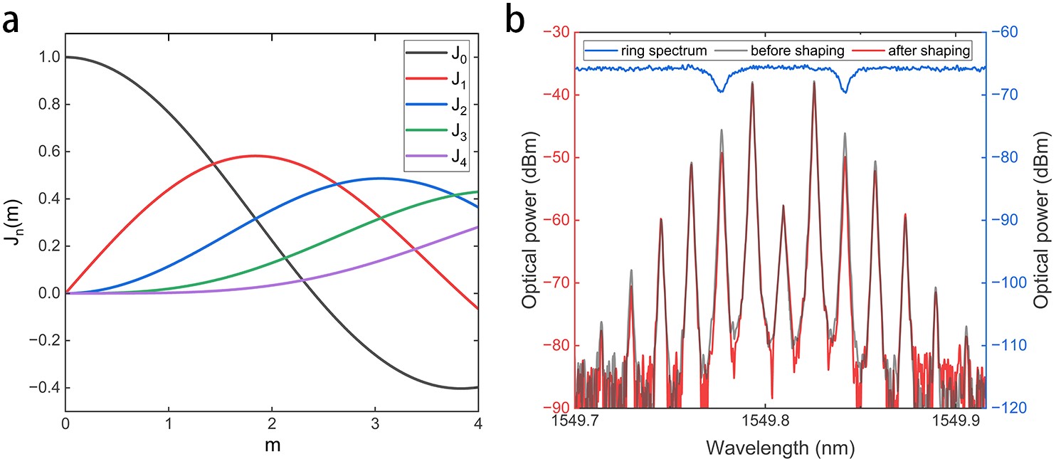
Supplementary Figure 1a shows the optical spectrum after the optical carrier passes through the modulator, with the 40 GHz sweep signal generated by the vector network analyzer (VNA) serving as the RF input. We utilized the maxhold function of the optical spectrum analyzer (OSA) to obtain the spectrum of the modulation sideband. Additionally, to get the half-wave voltage of the intensity modulator at high frequency, we employed the carrier maximization and sideband maximization methods. Our theoretical analysis is based on a push-pull Mach-Zehnder modulator (MZM), where the output of the optical carrier after modulation can be expressed as:
| (1) |
where represents the optical carrier with amplitude and frequency , is the phase shift induced by the RF signal, and is the phase shift induced by the DC bias.
| (2) |
where is the amplitude of RF signal, refers to the RF half-wave voltage. We introduce the modulation depth and utilize the Jacobi-Anger expansion , considering only small-signal modulation. At this point:
| (3) |
| (4) |
the modulated optical spectrum can be expressed as:
| (5) |
From the above equation (5), we can see that, for a given RF input power, the intensity of the carrier and sidebands after modulation is determined by the bias phase shift. When , the carrier intensity reaches its minimum value, and the sideband intensity reaches its maximum value. Conversely, when , the carrier intensity reaches its maximum value, and the sideband intensity reaches its minimum value. Supplementary Figure 1b shows the modulated optical spectrum at these two specific bias points with a 5 GHz RF signal input, where the ratio of maximum carrier intensity to maximum sideband intensity is 26.5 dB. Supplementary Figure 1c displays the ratio of sideband to carrier intensity for different modulation depth . In this case, is 0.095, and knowing the input voltage , we can calculate the half-wave voltage at 5 GHz.
Supplementary information ii: Programmable microrings
Supplementary Figure 2a is a microscope image of four cascaded microring resonators. As shown, the all-pass microrings use an MZI-assisted coupling structure. A characteristic of this coupling structure is that we can control the optical intensity at the output port by adjusting the phase in the interference arms. We achieve control of the microring resonance position by adjusting the phase shift in the racetrack region of the microrings. We use a multi-channel voltage source with an adjustment precision of 0.001V to apply voltage to the heaters through a 26-channel DC probe array, enabling precise control of the coupling state and resonance position of each microring.
By controlling the voltage applied to the coupling region, we can precisely manage the coupling state of each microring. When a microring is in a highly under-coupled state, the suppression ratio is zero, which can be understood as turning off the response of that microring. This allows us to easily control the number of resonance peaks, ranging from one to four peaks, corresponding to the responses in Supplementary Figures 2b to 2e, respectively. Supplementary Figure 2f shows the optical spectrum when we achieve a dual-band notch filter. We configured two pairs of under-coupled and over-coupled microrings with identical suppression ratios and symmetric resonance positions with respect to the carrier. This demonstrates our ability to precisely control the resonance position, state, and depth of the microrings as needed. Supplementary Figure 2g presents the spectrum when we achieve an ultra-high dynamic range notch filter. Over-coupled and under-coupled microrings with identical suppression ratios and symmetric resonance positions are used for filtering, and an over-coupled microring is used to process the optical carrier.
Supplementary information iii: Noise Figure
The Noise Figure (NF) is a critical parameter for evaluating the performance of RF systems. It quantifies the noise added by the system relative to an ideal noise source. An ideal system has a noise figure of 0 dB, indicating that the system introduces no additional noise. However, in practical applications, all components introduce some degree of noise. The noise figure is calculated using the following equation:
| (6) |
where is the system noise power, representing the total noise power in the system when no signal is present. This includes thermal noise, phase noise, and other internal noise sources. is the system’s link gain. The constant 174 is a reference value, representing the thermal noise power density in 1 Hz bandwidth at room temperature.
For microwave photonic links based on intensity modulators, reducing the noise figure can be achieved by using low bias voltage. In our demonstration, we placed a low-noise Erbium-doped fiber amplifier (EDFA) before the photodetector (PD). This is the optimal choice for amplifying the optical signal to achieve higher link gain. However, the downside is that the amplified spontaneous emission (ASE) noise from the EDFA directly enters the photodetector and is detected. In this scenario, ASE noise becomes the primary source of system noise, and adjusting the bias voltage has little impact on the overall noise figure. We tested the system’s link gain and noise at 1 GHz under different bias voltages and calculated the noise figure. As shown in Supplementary Figure 3, the link gain and noise exhibit the same trend with variations in bias voltage, while the noise figure remains relatively stable.
Supplementary information iv: Linearization method
When the optical carrier is modulated by a two-tone RF signal with frequency of , , Considering only the 0th to 2nd order sidebands generated by intensity modulation, and using the Jacobi-Anger expansion, the output of the modulator’s upper arm can be expressed as:
| (7) |
the output of the modulator’s lower arm can be expressed as:
| (8) |
in the above equation (7) and (8), we used . After combining the upper and lower arms, and after the optical carrier is processed by the microring, the output can be expressed as:
| (9) |
where is the transmission coefficient and is the phase shift of the microring.
The photocurrent of the RF signal detected from the processed optical spectrum can be expressed as:
| (10) |
where is the responsivity of the photodetector, and are the amplitudes of the fundamental signal and the IMD3 components, respectively. Let the modulator operate at the quadrature point, at which and can be written as:
| (11) |
| (12) |
when , , and can be expressed as:
| (13) |
| (14) |
To minimize the IMD3, a proper combination of and is needed. The best suppression happens under the condition:
| (15) |
To satisfy the requirements of the equation (15), we need to operate the microring in an over-coupled state and precisely control the position of the microring resonance peaks relative to the optical carrier. Additionally, from the equation (13) and (14), it can be observed that when IMD3 is perfectly suppressed, the fundamental signal will also be reduced to some extent, which is unavoidable.
Supplementary information v: Large interference signal suppression method
When a high-power RF signal with a frequency of is input into the intensity modulator, the small-signal modulation model is no longer applicable. We need to consider the 0th to 3rd order sidebands generated by modulation. Using the Jacobi-Anger expansion, the output of the modulator’s upper arm can be expressed as:
| (16) |
the output of the modulator’s lower arm can be expressed as:
| (17) |
Due to the high-order modulation sidebands generated by large-signal modulation, the beat frequencies of the first-order sideband and the carrier, the second-order sideband and the first-order sideband, and the third-order sideband and the second-order sideband will all produce the fundamental signal. However, the fundamental signal generated by the beat frequencies of different elements has different phases. We exploit this by using the microring response to process the high-order sidebands, thereby suppressing the high-power interference signal. Additionally, since low-power RF signals do not generate high-order modulation sidebands, small signals remain unaffected.
Assuming the transmission coefficient of the microring for the second-order sideband is and the induced phase shift is . For the third-order sideband, the transmission coefficient is and the induced phase shift is . Let the modulator operate at the quadrature bias point. The optical spectrum after being processed by the microring can be expressed as:
| (18) |
The photocurrent generated by the beat frequency between the first-order sideband and the carrier:
| (19) |
The photocurrent generated by the beat frequency between the first-order sideband second-order sideband:
| (20) |
The photocurrent generated by the beat frequency between the second-order sideband third-order sideband:
| (21) |
When , we achieve perfect suppression of the high-power interference signal. We only utilize the microring response to process the second-order sidebands, disregarding the effects of and . Suppression can occur when the following condition is satisfied:
| (22) |
Supplementary Figure 4a shows the relationship curve between modulation depth and . When the RF input power is constant, we can determine the corresponding modulation depth from the optical spectrum. This allows us to calculate the specific microring response needed to achieve suppression. Supplementary Figure 4b shows the optical spectrum corresponding to the suppression of the high-power interference signal. We utilize the response of two micro-rings to process the second-order modulation sidebands.