Valley separation of photoexcited carriers in bilayer graphene
Abstract
We derive the angular generation density of photoexcited carriers in gapless and gapped Bernal bilayer graphene. Exploiting the strong anisotropy of the band structure of bilayer graphene at low energies due to trigonal warping, we show that charge carriers belonging to different valleys propagate to different sides of the light spot upon photoexcitation. Importantly, in this low-energy regime, inter-valley electron-phonon scattering is suppressed, thereby protecting the valley index. This optically induced valley polarisation can be further enhanced via momentum alignment associated with linearly-polarised light. We then consider gapped bilayer graphene (for example with the gap induced by external top- and back-gates) and show that it exhibits valley-dependent optical selection rules with circularly-polarised light analogous to other gapped Dirac materials, such as transition metal dichalcogenides. Consequently, gapped bilayer graphene can be exploited to optically detect valley polarisation. Thus, we predict an optical valley Hall effect - the emission of two different circular polarisations from different sides of the light spot, upon linearly-polarised excitation. We also propose two realistic experimental setups in gapless and gapped bilayer graphene as a basis for novel optovalleytronic devices operating in the elusive terahertz regime.
I Introduction
Valleytronics is an emerging technology that seeks to exploit the local extrema (known as valleys) in the electronic band structure of materials for the storing and processing of quantum information schaibley2016valleytronics ; vitale2018valleytronics . Many crystalline solids exhibit energy-degenerate valleys in their band structure, but selectively addressing the valleys in conventional semiconductors is usually very difficult, making them impractical for valleytronic devices.
However, since the exfoliation of graphene in 2004, investigation into two-dimensional (2D) materials has shown that they are promising candidates for valleytronics, due to their often strong valley-dependent interactions with applied electric and magnetic fields. Indeed, graphene has an electronic band structure characterised by two inequivalent massless Dirac cones (valleys) at the corners of the Brillouin zone katsnelson2020physics . The well defined valley quantum number of electrons in graphene spurred research into its feasibility for valleytronics. The first proposals for valleytronic applications in graphene were confined to the electronic transport regime. It was soon discovered that atomic scale defects at the edges of realistic devices mix the valleys, hampering the potential for valleytronics in electronic transport.
An alternative path to valleytronics involves selective optical excitations of charge carriers in the bulk of 2D materials. However, the inversion symmetry of pristine graphene results in valley-independent optical selection rules for interband transitions at low energy, posing a challenge for the creation and measurement of valley polarisation. At higher excitation energies, when trigonal warping in the graphene spectrum becomes important, charge carriers in different valleys can be spatially separated in the instance of photocreation hartmannthesis ; saroka2022momentum . However, this anisotropy in the band structure occurs well above the energy of associated with ultra-fast inter-valley electron-phonon scattering phononscattering , that dramatically reduces the lifetime of the valley quantum number and makes the effect impractical for quantum valleytronics.
The inversion symmetry of graphene may be broken by placing the sample on a matching substrate which makes the two sublattice sites inequivalent, such as boron nitride boron . This opens a band gap in the electronic dispersion resulting in strong valley-dependent optical selection rules. Electrons in one valley may be selectively excited by circularly-polarised light of a given handedness saroka2022momentum . This effect is well-known in other 2D gapped Dirac materials, such as transition metal dichalcogenides (TMDs) schaibley2016valleytronics . Valley population in gapped Dirac materials may indeed be controlled by the degree of circular polarisation, however, purely optical spatial separation of charge carriers belonging to different valleys is not possible in the absence of warping. Moreover, opening the gap in Dirac materials results in low carrier mobility that affects the ability to propagate the valley index boron2 ; TMD .
In this paper, we propose a method to optically induce and detect sustainable spatial separation of charge carriers from different valleys in a high mobility, gapless Dirac material: Bernal-stacked bilayer graphene. There is currently a resurgence of interest in this material, with recent research revealing a variety of new effects, including many-body phase transitions and superconductivity bilayersuperconductivity ; bilayercorrelated ; bilayermanybody . We consider low-frequency photoexcitation in bilayer graphene that has been overlooked so far. In contrast to monolayer graphene, the valleys of bilayer graphene are highly anisotropic at the scale. Firstly, we show that this anisotropy can be exploited to induce spatial separation of charge carriers belonging to different valleys by illuminating the sample with low-frequency photons. This valley polarisation may be further enhanced by exploiting momentum alignment with linearly-polarised light. In stark contrast to monolayer graphene, this effect occurs at low excitation energies where inter-valley phonon scattering is suppressed, thereby preserving the topological protection of the valley index in view of novel valleytronic applications. We subsequently demonstrate that the valley-dependent spatial separation of charge carriers persists even after opening a moderate band gap in the electronic dispersion. Finally, we show that gapped bilayer graphene exhibits valley-dependent optical selection rules with circularly polarised light similar to those of other gapped 2D Dirac materials. These selection rules can be exploited to detect the degree of valley polarisation induced after the spatial separation of charge carriers.
By combining these phenomena, we propose two experimental setups to optically induce and detect valley separation in conventional bilayer graphene devices routinely available in experimental labs worldwide.
II Bilayer Graphene
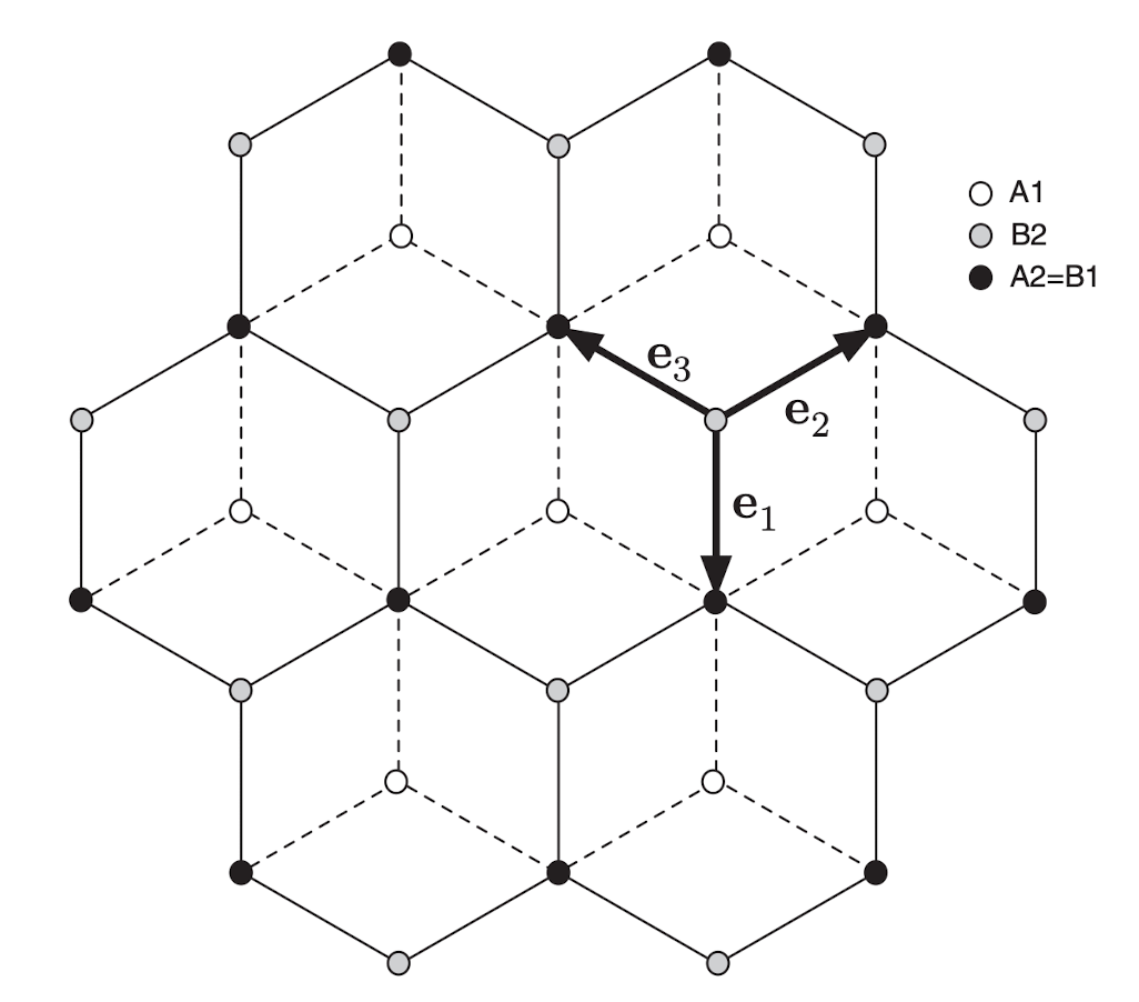
The crystal structure of Bernal-stacked bilayer graphene is shown in Fig. 1. The second layer is shifted with respect to the first so that the atoms of sublattice A in layer 2 (A2) are located directly above atoms of sublattice B in layer 1 (B1), at a distance . The pairs A1-A2, B1-B2 and A1-B2 are all separated by the distance where is the nearest-neighbour distance in monolayer graphene Mariani2012 .
The electronic properties of bilayer graphene can be analysed using the tight-binding Hamiltonian
| (1) |
keeping only the dominant terms relevant for describing the low-energy sector. The basis of electron states is , where is the amplitude of the wavefunction on the sublattice and layer . The term for the wavevector , with the nearest-neighbour vectors , , and , as shown in Fig. 1. The hopping terms are , , and mccann2013electronic .
In the vicinity of the two inequivalent Dirac points (or valleys) , the Hamiltonian in Eq. (1) can be expanded as
| (2) |
and
| (3) |
where the superscripts and refer to the valleys. Here, is the complex representation of the two-dimensional quasi-momentum relative to the Dirac point, for , such that , and .
An effective Hamiltonian at low energies can be derived for each valley using the Schrieffer-Wolff transformation bravyi2011schrieffer (see Appendix for a derivation). This gives the Hamiltonian
| (4) |
where refers to the valley (either or ),
| (5) |
and
| (6) |
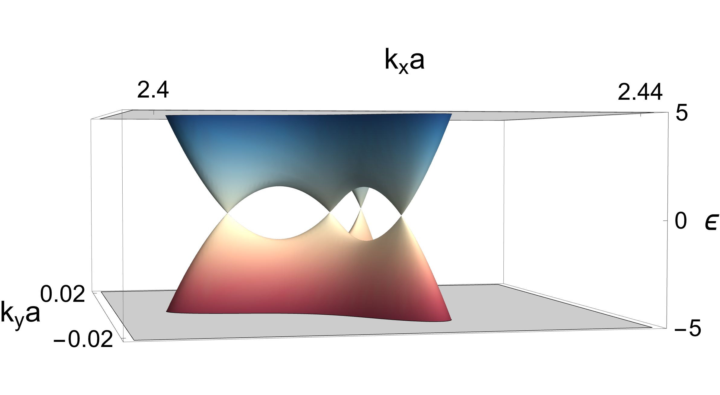
The terms proportional to are associated with trigonal warping that produces a qualitative restructuring of the low energy electronic band structure (see Fig. 2 (upper panel)). This will have dramatic consequences on the photoexcitation properties of the system.
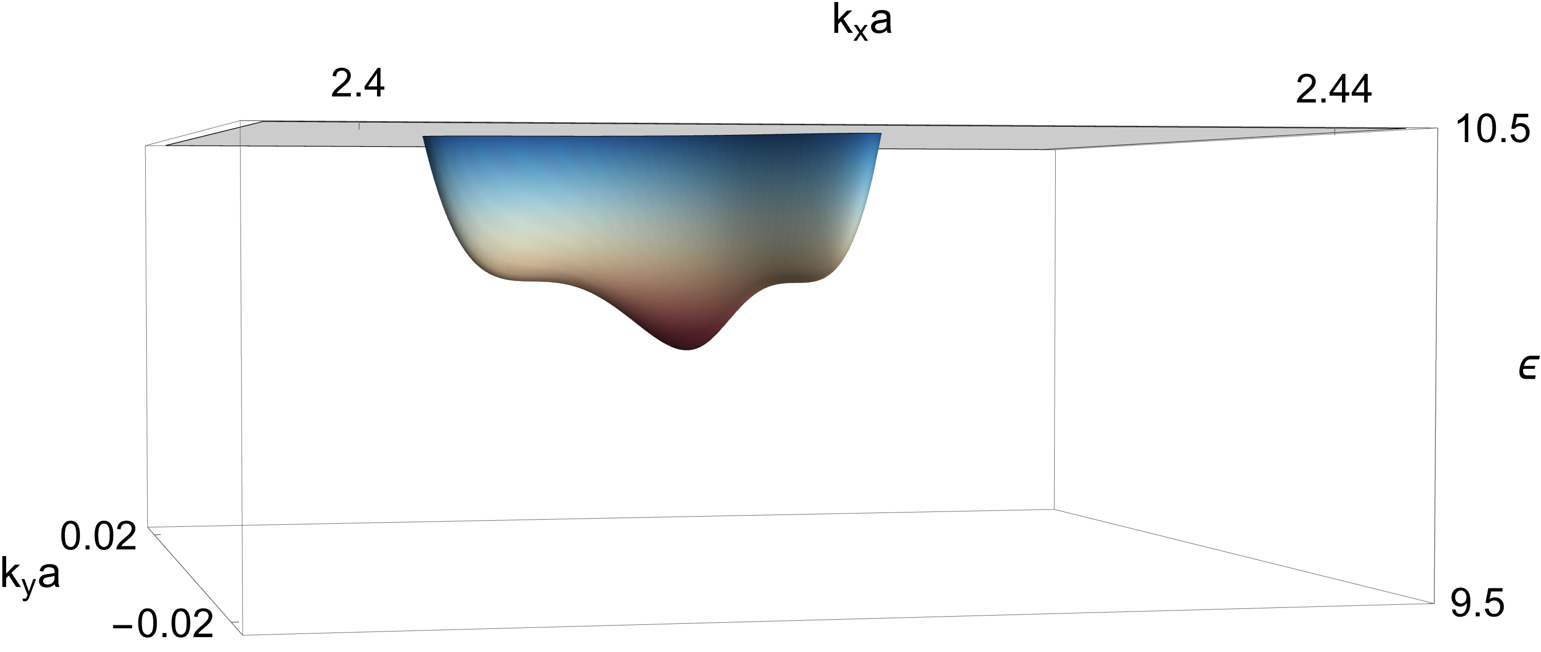
Figure 2 (upper panel) shows the eigenenergies (7) for the valley up to . At these low energies, the band structure is characterised by four mini-Dirac cones that merge into singly-connected equipotential domains above the Lifshitz transition energy of order . This valley-dependent highly anisotropic band structure survives up to energies of order as shown by the equipotential lines in Fig. 2 (lower panel). We will show in section IV.1 that this phenomenon may be exploited to create valley separation of charge carriers in bilayer graphene.
A band gap can be opened in bilayer graphene by applying an electric field perpendicular to the layers zhang2009bilayer . The low-energy properties of gapped bilayer graphene with a band gap of can be analysed by introducing two diagonal terms into the effective low-energy Hamiltonian (4)
| (9) |
where
| (10) |
The eigenenergies and normalised eigenstates of the Hamiltonian (9) are
| (11) |
and
| (12) |
where . For convenience of notation, from now on we will drop the explicit dependencies on .
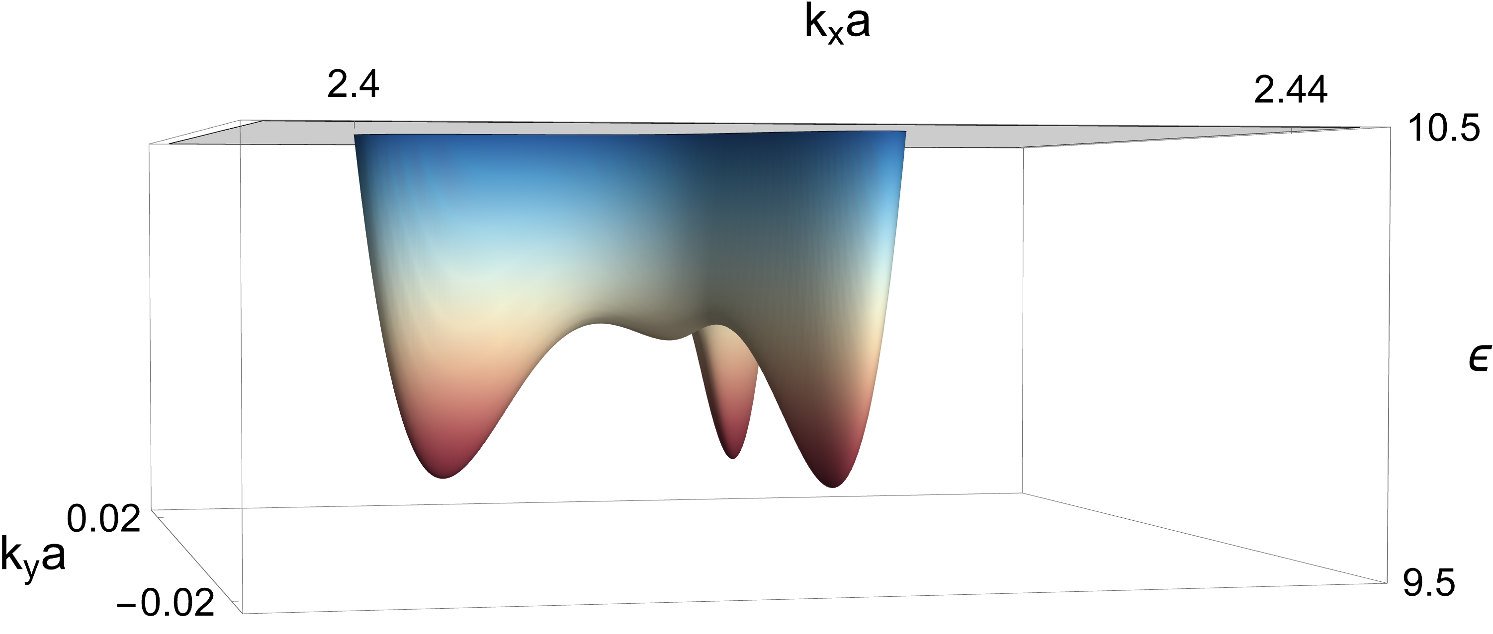
Figure 3 shows the low-energy conduction band of gapped bilayer graphene with a band gap of in the THz frequency range. Including only and lower-order hopping terms results in a shallow central minimum surrounded by three satellite minima at lower energy, as shown in the upper panel. Including higher-order skew interlayer hopping terms, parametrised by the hopping energy , has the effect of raising the three satellite minima, as shown in the lower panel. Depending on the value of , which is not precisely known, the three satellite minima may rise above the central one. According to McCann mccann2013electronic , , which indeed results in a central global minimum at the points. It should be noted that the inclusion of the terms does not affect the main results of this work, in particular the ability to separate photo-excited carriers from different valleys and to detect them, as discussed below.
III Optical Selection Rules For Bilayer Graphene
III.1 Gapless Bilayer Graphene
We now derive the matrix elements for optical transitions in pristine bilayer graphene. In the dipole approximation, the transition rate of an electron, of wave vector , from the valence band to the conduction band is given by Fermi’s golden rule:
| (13) |
where and are the eigenstates of the electrons in the conduction and valence bands, and and are the corresponding energies. Here, is the fine-structure constant, while , , and are the velocity operator, intensity and frequency of the excitation, respectively. The vector describes the polarisation of the excitation, which we assume to propagate normal to the surface of the crystal saroka2022momentum ; hartmannthesis . Within the gradient approximation, the velocity operator is deduced from the effective Hamiltonian (4) as
| (14) |
where . Thus, the optical selection rules of our system stem from the matrix element given by
| (15) |
where denotes the imaginary part.
III.2 Gapped Bilayer Graphene
The approach above can be generalised to deduce the optical section rules for gapped bilayer graphene as well. The matrix element for optical transitions for the Hamiltonian (9) is
| (16) |
where denotes the real part. This reduces to the gapless result in Eq. (15) in the limit .
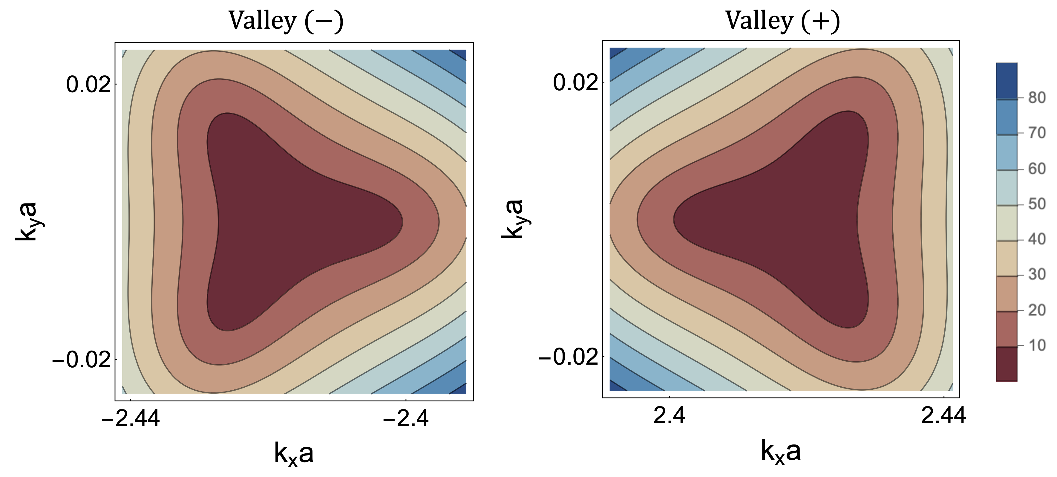
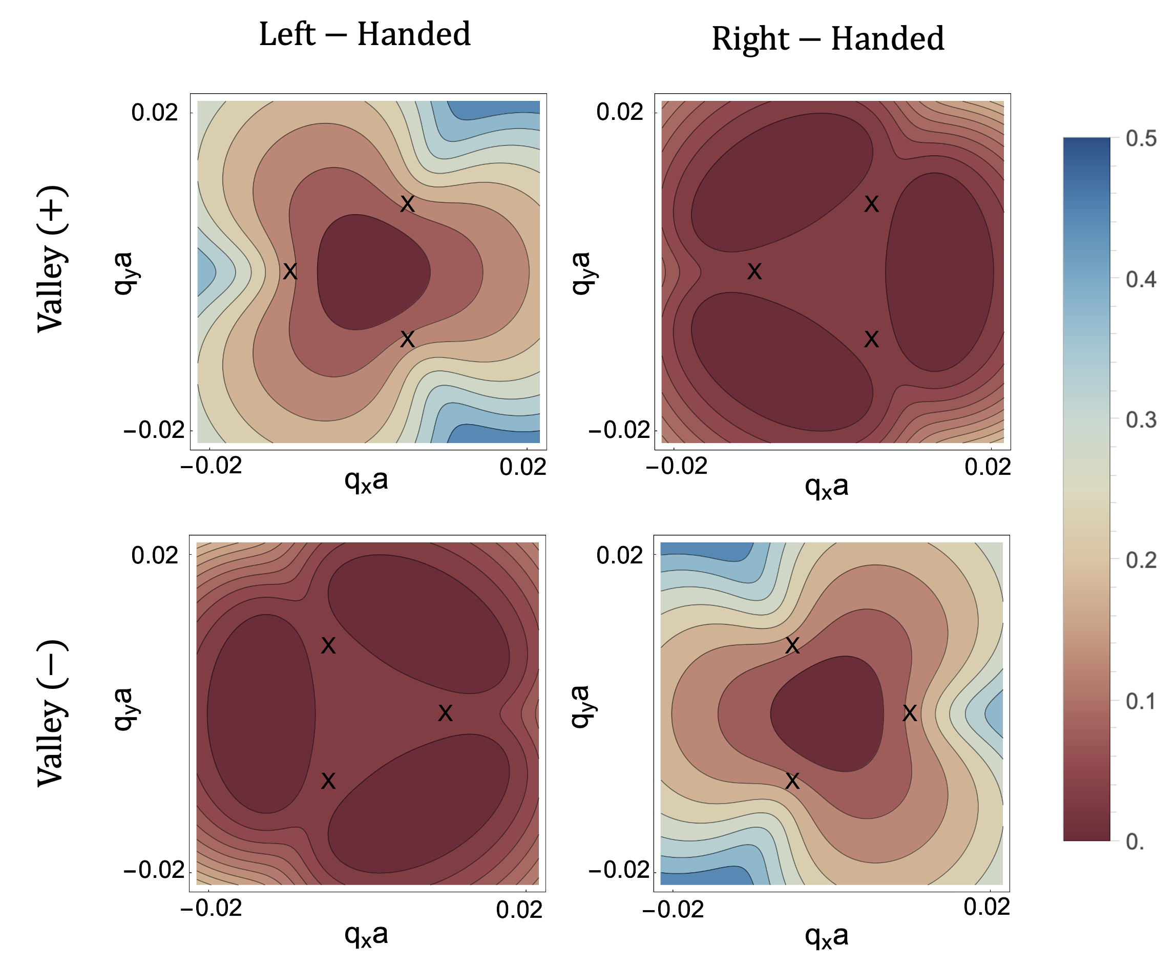
Figure 4 shows contour plots of the modulus-square of the matrix element (16), for the circular polarisations , with . The and correspond to left- and right-handed circular polarisations, respectively. There is a clear coupling between the valley index and the handedness of circularly-polarised light associated with optical transitions in gapped bilayer graphene.
The presence of trigonal warping is directly evident in the angular dependence of the matrix element. Moreover, the linear terms in in the effective Hamiltonian, proportional to , induce a crossover between the selection rules as a function of . Indeed, in the valley (upper row in Fig. 4) the optical transitions are dominated by the right-handed circular polarisation at the point () and by the left-handed circular polarisation at larger momenta. The effect is opposite in the valley (lower row in Fig. 4). Notice that this crossover would not be present if trigonal warping was neglected, as conventionally done in the literature.
These valley-dependent selection rules can be exploited to detect the degree of valley polarisation in gapped bilayer graphene by measuring the handedness of circularly-polarised light emitted across the sample. We will discuss this detection method in Sec. IV.2 below.
IV Optovalleytronics in Bilayer Graphene
IV.1 Angular Generation Density of Photoexcited Carriers in Bilayer Graphene
We will now use the matrix element given in Eq. (15) to derive the angular generation density of photoexcited carriers in the instance of photocreation in bilayer graphene.
The angular generation density is defined such that gives the rate of carriers per unit area created in the angle range to . For a single valley and spin, the angular generation density is given by saroka2022momentum
| (17) |
where . Combining Eqs. (13) and (15) with Eq. (17), and performing the integration numerically gives the angular distribution of photoexcited carriers in bilayer graphene.
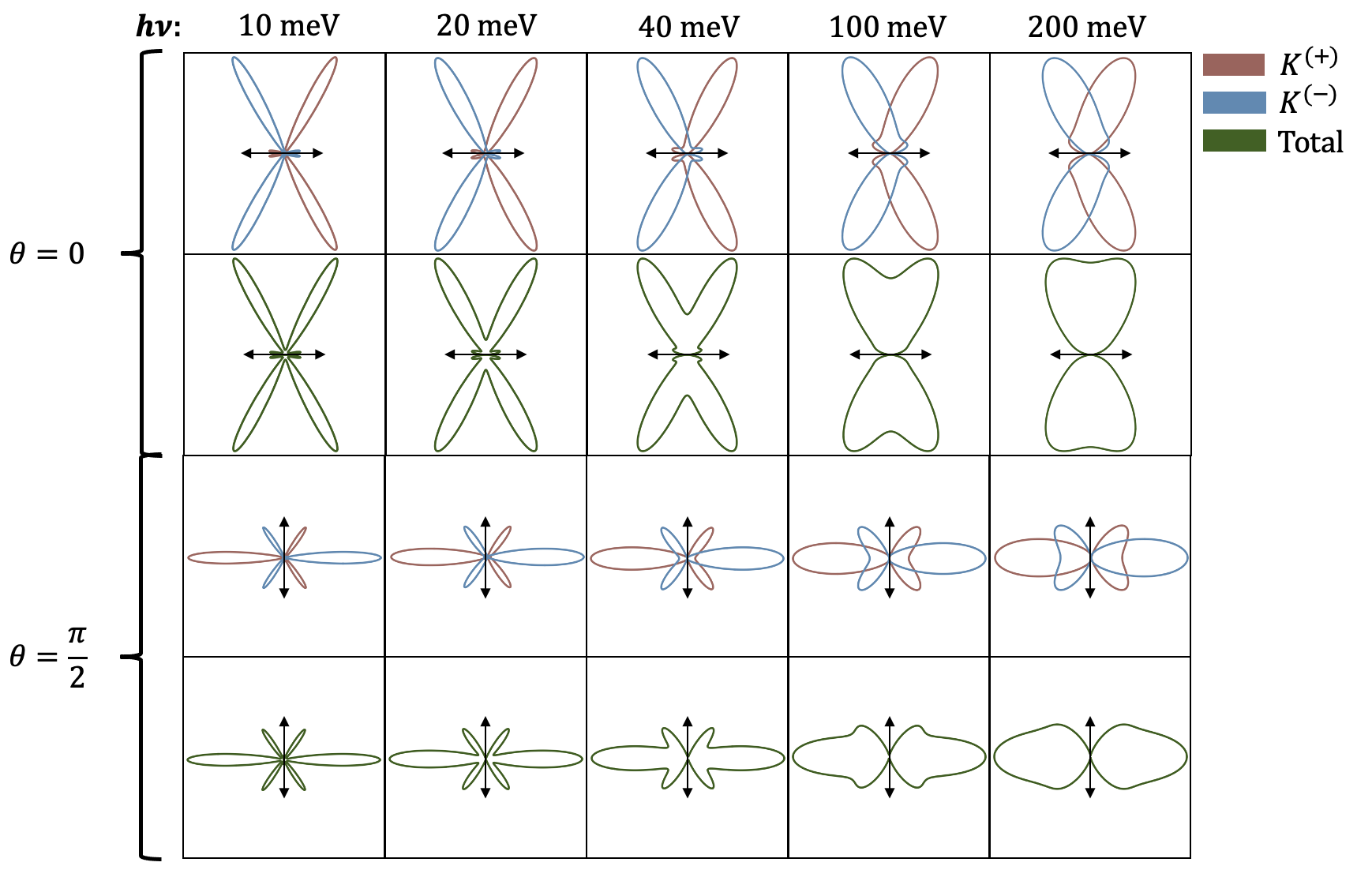
Figure 5 shows polar plots of for gapless bilayer graphene for linearly-polarised light at various excitation energies, for polarisation angles and . The red and blue plots show the contribution from the and valleys, respectively, while the green plots show their sum, and the double-headed black arrow represents the polarisation of the excitation.
It can be seen that at low energies, there is a large degree of valley separation, in the instance of photocreation. If the light has a polarisation angle of , the charge carriers propagate away from the light spot preferentially along the positive -axis for the valley and the negative -axis for the valley. Notice that, due to momentum alignment phenomena hartmannthesis ; saroka2022momentum , there are no carriers generated in the direction parallel to the polarisation plane of the light.
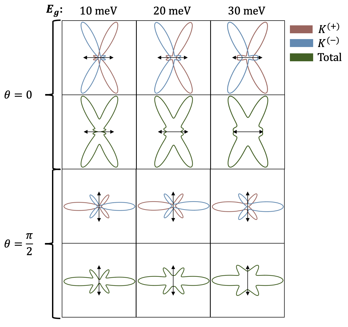
This valley separation persists even in the case of gapped bilayer graphene for experimentally attainable values of the band gap (), and photon excitation energies above , as shown in Fig. 6. Together with the selection rules for circularly-polarised light of gapped bilayer discussed in Sec. III.2, this leads to the optical valley Hall effect - the emission of two different circular polarisations from different sides of the light spot, upon linearly-polarised excitation.
It is important to stress that this asymmetry persists up to excitation energies exceeding where the low-energy restructuring due to trigonal warping is not as prominent. Therefore, we expect the observation of this effect to be robust against charge-density fluctuations due to local inhomogeneities. This valley separation mechanism may be used to independently manipulate charge carriers in different valleys, for potential use in future valleytronic devices.
IV.2 Basic Optovalleytronic Devices Using Bilayer Graphene
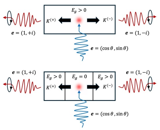
We now propose two rudimentary experimental setups exploiting the properties of gapless and gapped bilayer graphene derived in sections III.2 and IV.1 to create and measure valley separation. The two setups are illustrated in Fig. 7.
In the upper panel, there is a scheme for observing the optical valley Hall effect in uniformly-gapped bilayer graphene. Carriers should be excited by linearly-polarised light (red light spot in Fig. 7) above the band gap resulting in the anisotropic momentum and valley-index distribution, as shown in Fig. 6, and in the consequent spatial separation of the carriers from different valleys. For low enough excitation energies (below the inter-valley phonon energy), photoexcited carriers at the two opposite sides of the light spot will relax to the band edges (at the three satellite minima indicated by crosses in Fig. 4) retaining their valley index. The consequent edge photoluminescence will be dominated by left (right) -handed circular polarisation in the valley. To observe the effect, the sample should be doped (or gate-doped) so that photoexcited carriers recombine with their equilibrium counterparts. Thus, the valley index of minority carriers is detected.
Notice that this detection approach is robust against the inclusion of higher-order hopping terms. Depending on the value of (see Fig. 3), photoexcited carriers may instead relax to the band edges at the points. In this case, they would predominantly emit right (left) -handed circularly polarised light in the valley. Importantly, the degree of circular polarisation from opposite sides of the light spot would still be opposite for the two inequivalent valleys, allowing for the detection of the valley polarisation.
In the lower panel of Fig. 7, a central region of gapless bilayer graphene is surrounded by two gapped regions (induced by means of top- and back-gate voltages). In contrast to the previous setup, this device benefits from a higher mobility in the central gapless region. In this device, linearly-polarised light is shone onto gapless bilayer graphene, resulting in high-mobility charge carriers of different valley-index propagating into the two gapped regions. In any realistic setup, the gate-induced gap changes smoothly over length scales much larger than the lattice spacing, thereby preventing inter-valley mixing at the gapless-gapped interface. Circularly-polarised light of opposite handedness should then be emitted at the two different gapped regions. In both setups, the incident photon energy must be below the inter-valley phonon energy of to avoid inter-valley scattering.
We emphasise that our proposed setups: (i) exploit bulk properties of bilayer graphene and their functionality does not involve any edge effects that are known to deteriorate the valley index in conventional transport experiments; (ii) are based on conventional bilayer devices and excitation frequencies that have been available in the literature for over a decade zhang2009bilayer ; (iii) operate in the elusive terahertz regime, a frequency range critical for emerging technologies, including 6G communications, security screening, and advanced testing in pharmaceutical and biomedical applications.
V Conclusions
We find that, by exploiting the highly anisotropic nature of the electronic band structure of gapless and gapped bilayer graphene at low energies (), spatial separation of charge carriers in different valleys is possible using optical excitation with low-frequency photons. This effect can be enhanced via momentum alignment induced by linearly-polarised light. Importantly, in this low-energy regime, inter-valley electron-phonon scattering is suppressed, thereby protecting the valley index. This is in stark contrast to the band structure of monolayer graphene which only begins to deviate significantly from the isotropic conical dispersion near the Dirac points well above the inter-valley phonon energy of . Additionally, gapped bilayer graphene exhibits valley-dependent optical selection rules, which may be used to measure the degree of valley polarisation of the spatially separated charge carriers. We propose two realistic experimental setups which exploit these effects in gapless and gapped bilayer graphene as a basis for future optovalleytronic devices. Very recently, it has been experimentally shown that the valley states in bilayer graphene are long lived, with a lifetime one order of magnitude longer than conventional spin states Ensslin2024 . This makes bilayer graphene a highly promising platform for emerging quantum-optovalleytronics applications.
Acknowledgements.
This work was supported by the EU H2020-MSCA-RISE projects TERASSE (Project No. 823878) and CHARTIST (Project No. 101007896) as well as by the NATO Science for Peace and Security project NATO.SPS.MYP.G5860. M.E.P. acknowledges support from UK EPSRC (Grant No. EP/Y021339/1). E.M. acknowledges insightful discussions with Mauro and Roberta Bucanieri. For the purpose of open access, the authors have applied a CC BY public copyright licence to any Author Accepted Manuscript version arising from this submission.*
Appendix A Low Energy Effective Hamiltonian of Bilayer Graphene
In this Appendix, we derive the low energy effective Hamiltonian of bilayer graphene in Eq. (4), starting from the Hamiltonian (1). We use the Schrieffer-Wolff (SW) transformation bravyi2011schrieffer to decouple the Hamiltonian into low- and high-energy subspaces. For our purposes with bilayer graphene, this corresponds to deriving a Hamiltonian for the two bands shown in Fig. 2 (upper panel) which touch close to zero energy, whilst neglecting the other two that correspond to higher energy excitations of order . For our analysis, the relevant low-energy subspace is A1-B2 Mariani2012 .
In the SW transformation, we begin with a Hamiltonian of the form
| (18) |
where describes the unperturbed low-energy subspace, and is a small perturbation.
We now perform a unitary transformation, using the unitary operator , with the generator , to obtain the Hamiltonian , given by
| (19) |
such that is anti-hermitian, . For small V, the generator S will be small and we may expand to second-order. We have
| (20) |
Therefore,
| (21) |
which is a special case of the Baker-Campbell-Hausdorff formula.
can be made diagonal to first order in by choosing such that . Substituting this condition into Eq. (21) gives
| (22) |
which is the standard form of the SW transformation.
In second quantisation, the Hamiltonian (1) written in the form of Eq. (18) has
| (23) |
| (24) |
where we have introduced the creation (annihilation) operators () which add (remove) electrons on the A/B site in the 1st/2nd layer, respectively. These creation and annihilation operators fulfill the anticommutation relations
| (25) |
where is the Kronecker delta.
After finding the generator S which satisfies the condition , the commutator can be computed and substituted into Eq. (22) giving . Keeping only those terms in the low-energy subspace A1-B2 we obtain the low-energy effective Hamiltonian
| (26) |
References
- (1) J. R. Schaibley, H. Yu, G. Clark, P. Rivera, J. S. Ross, K. L. Seyler, W. Yao, X. Xu, Valleytronics in 2D materials, Nat. Rev. Mater. 1, 16055 (2016).
- (2) S. A. Vitale, D. Nezich, J. O. Varghese, P. Kim, N. Gedik, P. Jarillo-Herrero, D. Xiao, M. Rothschild, Valleytronics: opportunities, challenges, and paths forward, Small 14, 1801483 (2018).
- (3) M. I. Katsnelson, The physics of graphene (Cambridge University Press, Cambridge, 2020).
- (4) R. R. Hartmann, M. E. Pornoi, Optoelectronic properties of carbon-based nanostructures: steering electrons in graphene by electromagnetic fields, (LAP Lambert Academic Publishing, Saarbrücken, 2011).
- (5) V. A. Saroka, R. R. Hartmann, M. E. Portnoi, Momentum alignment and the optical valley Hall effect in low-dimensional Dirac materials, J. Exp. Theor. Phys. 135, 513 (2022).
- (6) J.-A. Yan, W. Y. Ruan, M. Y. Chou, Phonon dispersions and vibrational properties of monolayer, bilayer, and trilayer graphene: density-functional perturbation theory, Phys. Rev. B 77, 125401 (2008).
- (7) M. Yankowitz, J. Xue, B. J. LeRoy, Graphene on hexagonal boron nitride, J. Condens. Matter Phys. 26, 303201 (2014).
- (8) J. Wang, F. Ma, M. Sun, Graphene, hexagonal boron nitride, and their heterostructures: properties and applications, RSC Adv. 7, 16801 (2017).
- (9) S. Manzeli, D. Ovchinnikov, D. Pasquier, O. V. Yazyev, A. Kis, 2D transition metal dichalcogenides, Nat. Rev. Mater. 2, 17033 (2017)
- (10) H. Zhou, L. Holleis, Y. Saito, L. Cohen, W. Huynh, C. L. Patterson, F. Yang, T. Taniguchi, K. Watanabe, A. F. Young, Isospin magnetism and spin-polarized superconductivity in Bernal bilayer graphene, Science 375, 774 (2022).
- (11) A. M. Seiler, F. R. Geisenhof, F. Winterer, K. Watanabe, T. Taniguchi, T. Xu, F. Zhang, R. Thomas Weitz, Quantum cascade of correlated phases in trigonally warped bilayer graphene, Nature 608, 298 (2022).
- (12) P. A. Pantaleón, A. Jimeno-Pozo, H. Sainz-Cruz, V. T. Phong, T. Cea, F. Guinea, Superconductivity and correlated phases in non-twisted bilayer and trilayer graphene, Nat. Rev. Phys. 5, 304 (2023).
- (13) E. Mariani, A. J. Pearce, F. von Oppen, Fictitious gauge fields in bilayer graphene, Phys. Rev. B 86, 165448 (2012).
- (14) E. McCann, M. Koshino, The electronic properties of bilayer graphene, Rep. Prog. Phys. 76, 056503 (2013).
- (15) S. Bravyi, D. P. DiVincenzo, D. Loss, Schrieffer-Wolff transformation for quantum many-body systems, Ann. Phys. 326, 2793 (2011).
- (16) Y. Zhang, T. T. Tang, C. Girit, Z. Hao, M. C. Martin, A. Zettl, M. F. Crommie, Y. R. Shen, F. Wang, Direct observation of a widely tunable bandgap in bilayer graphene, Nature 459, 820 (2009).
- (17) R. Garreis, C. Tong, J. Terle, M. J. Ruckriegel, J. D. Gerber, L. M. Gächter, K. Watanabe, T. Taniguchi, T. Ihn, K. Ensslin, and W. W. Huang, Long-lived valley states in bilayer graphene quantum dots. Nat. Phys. 20, 428 (2024).