thanks: These authors contributed equallythanks: These authors contributed equallythanks: These authors contributed equallythanks: These authors contributed equally

Supplementary Material for
“Group delay controlled by the decoherence of a single artificial atom"

Y.-T. Cheng Department of Physics, City University of Hong Kong, Kowloon, Hong Kong SAR 999077, China    K.-M. Hsieh Department of Physics, City University of Hong Kong, Kowloon, Hong Kong SAR 999077, China    B.-Y. Wu Department of Physics, City University of Hong Kong, Kowloon, Hong Kong SAR 999077, China    Z. Q. Niu State Key Laboratory of Materials for Integrated Circuits, Shanghai Institute of Microsystem and Information Technology (SIMIT), Chinese Academy of Sciences, Shanghai 200050, China ShanghaiTech University, Shanghai 201210, China    F. Aziz Department of Physics, National Tsing Hua University, Hsinchu 30013, Taiwan    Y.-H. Huang Department of Physics, National Tsing Hua University, Hsinchu 30013, Taiwan    P. Y. Wen Department of Physics, National Chung Cheng University, Chiayi 621301, Taiwan    K.-T. Lin CQSE, Department of Physics, National Taiwan University, Taipei 10617, Taiwan    Y.-H. Lin Department of Physics, National Tsing Hua University, Hsinchu 30013, Taiwan Center for Quantum Technology, National Tsing Hua University, Hsinchu 30013, Taiwan    J. C. Chen Department of Physics, National Tsing Hua University, Hsinchu 30013, Taiwan Center for Quantum Technology, National Tsing Hua University, Hsinchu 30013, Taiwan    A. F. Kockum Department of Microtechnology and Nanoscience (MC2), Chalmers University of Technology, SE-412 96 Gothenburg, Sweden    G.-D. Lin CQSE, Department of Physics, National Taiwan University, Taipei 10617, Taiwan Physics Division, National Center for Theoretical Sciences, Taipei 10617, Taiwan    Z.-R. Lin zrlin@mail.sim.ac.cn State Key Laboratory of Materials for Integrated Circuits, Shanghai Institute of Microsystem and Information Technology (SIMIT), Chinese Academy of Sciences, Shanghai 200050, China    Y. Lu kdluyong@outlook.com Guangzhou Institute of technology, Xidian University, Xi’an, China Advanced Interdisciplinary Research Center, Xidian University, Xi’an, China Faculty of Integrated Circuit, Xidian University, Xi’an, China    I.-C. Hoi iochoi@cityu.edu.hk Department of Physics, City University of Hong Kong, Kowloon, Hong Kong SAR 999077, China
(October 5, 2024)

S1 Experimental setup

The experimental setups used for conducting the measurements described in the main text are shown in Fig. S1. For the frequency-domain measurement, a vector network analyzer (VNA) is employed to transmit and receive the continuous-wave (CW) signal. The time-domain measurement instead employs an in-phase-and-quadrature (IQ) modulated radiofrequency (RF) source driven by an arbitrary-waveform generator (AWG) serving as the transmitter, while a digitizer, along with a down-converting mixer and an RF source, functions as a heterodyne receiver. To combine the frequency- and time-domain measurement systems, two splitters are used at the input and output ports of the dilution refrigerator (DR) at room temperature. These systems generate the probe tone for different types of measurements. Furthermore, an RF source acts as a control tone and is combined with the probe tone using the same splitter functioning as a combiner at the input port of the DR.

Refer to caption
Figure S1: Measurement setup and device images. (a) The frequency- and time-domain measurement systems are combined together using splitters. The device under test (orange dashed box) is positioned at the bottom of the dilution refrigerator, operating at a base temperature of 10 mK (blue dashed box). (b) Optical microscope and scanning electron microscope (SEM) images of Device 1: the transmon-type artificial atoms [1] are highlighted by the red boxes with enlarged views, while an SEM image displays the Josephson junctions forming a superconducting quantum interference device (SQUID), depicted in the green box. The capacitance at the end of the transmission line serves as a mirror. The orange dashed box contains the equivalent circuit of the device. (c) Optical microscope and SEM images of Device 2: the transmon-type artificial atom is capacitively coupled to the end of the transmission line as shown in the image. An SEM image displays the Josephson junctions forming a SQUID, indicated in the green box. The atom is positioned at the mirror with L=0𝐿0L=0, ensuring that the atom is at the antinodes of electric fields in the waveguide.

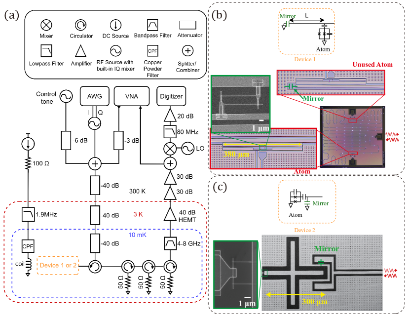
The combined input signal is directed towards the device, which consists of the atom-mirror system (orange dashed box) situated in a dilution refrigerator (blue dashed box) at a base temperature of T=10mK𝑇10mKT=10\,\mathrm{mK}. This low temperature ensures that the atom has a negligible thermal population (kBTω10much-less-thansubscript𝑘𝐵𝑇Planck-constant-over-2-pisubscript𝜔10k_{B}T\ll\hbar\omega_{10}, where kBsubscript𝑘𝐵k_{B} is Boltzmann’s constant) and therefore is in its ground state when an experiment begins. After interacting with the atom, the reflected signal undergoes amplification and filtering processes before returning to room temperature. The signal is split in half by the splitter and directed to the receiver parts of the two measurement systems separately.

In the DR, two devices are measured individually and undergo identical characterization procedures. Device 1 [see Fig. S1(b)] incorporates an artificial atom positioned at a distance L66mm𝐿66mmL\approx 66\,\mathrm{mm} from the mirror. By adjusting the global magnetic flux to set the flux through the superconducting quantum interference device (SQUID) formed by the Josephson junctions of the artificial atom, we modify the transition frequencies ω10subscript𝜔10\omega_{10} such that the atom can be selectively positioned at either an antinode or a node of the resonant electric field. In contrast, Device 2 [see Fig. S1(c)] features an artificial atom positioned at the mirror (L=0𝐿0L=0), which always is at the antinode of the electric field.

S2 Reflection coefficient as a function of probe power and probe frequency

In this section, we first perform reflection spectroscopy with a single tone on Devices 1 and 2 to extract parameters of the |0|1ket0ket1|0\rangle\leftrightarrow|1\rangle transition: the transition frequency ω10subscript𝜔10\omega_{10}, the relaxation rate Γ10subscriptΓ10\Gamma_{10}, the decoherence rate γ10subscript𝛾10\gamma_{10}, and the atom-field coupling constant k10subscript𝑘10k_{10}. Next, we investigate the phenomenon of positive and negative group delays using a weak continuous probe in the frequency domain.

For a continuous probe of frequency ωpsubscript𝜔𝑝\omega_{p} interacting with an atom in front of a mirror, the reflection coefficient is given by [2]

r=1Γ10γ101i(δp,10/γ10)1+δp,102/γ102+Ωp2/Γ10γ10,𝑟1subscriptΓ10subscript𝛾101𝑖subscript𝛿𝑝10subscript𝛾101superscriptsubscript𝛿𝑝102superscriptsubscript𝛾102superscriptsubscriptΩ𝑝2subscriptΓ10subscript𝛾10r=1-\frac{\Gamma_{10}}{\gamma_{10}}\frac{1-i\left(\delta_{p,10}/\gamma_{10}\right)}{1+\delta_{p,10}^{2}/\gamma_{10}^{2}+\Omega_{p}^{2}/\Gamma_{10}\gamma_{10}}, (S1)

where δp,10=ωpω10subscript𝛿𝑝10subscript𝜔𝑝subscript𝜔10\delta_{p,10}=\omega_{p}-\omega_{10} is the detuning between the probe frequency and the atom resonance frequency, and ΩpsubscriptΩ𝑝\Omega_{p} is the Rabi frequency of the probe, which is proportional to the voltage amplitude Vpsubscript𝑉𝑝V_{p} of the probe, or, equivalently, to the square root of chip-level power Ppsubscript𝑃𝑝P_{p}, i.e., Ωp=k10PpsubscriptΩ𝑝subscript𝑘10subscript𝑃𝑝\Omega_{p}=k_{10}\sqrt{P_{p}}. The non-radiative decay rate of the atom is

Γ10n=γ10Γ10/2,subscriptsuperscriptΓ𝑛10subscript𝛾10subscriptΓ102\Gamma^{n}_{10}=\gamma_{10}-\Gamma_{10}/2, (S2)

and is defined to contain both pure dephasing and intrinsic loss (i.e., decay to other environments than the transmission line).

If a weak probe (Ωpγ10much-less-thansubscriptΩ𝑝subscript𝛾10\Omega_{p}\ll\gamma_{10}) is used, Eq. (S1) becomes Eq. (1) in the main text. Furthermore, if the probe also is resonant (δp,10=0subscript𝛿𝑝100\delta_{p,10}=0), Eq. (S1) becomes

r=1Γ10γ10.𝑟1subscriptΓ10subscript𝛾10r=1-\frac{\Gamma_{10}}{\gamma_{10}}. (S3)

In the case of strong coupling, where Γ10Γ10nmuch-greater-thansubscriptΓ10subscriptsuperscriptΓ𝑛10\Gamma_{10}\gg\Gamma^{n}_{10}, Eq. (S2) is simplified and incorporated into Eq. (S3), resulting in r=1𝑟1r=-1. It thus turns out that a resonant weak probe field is fully reflected with a π𝜋\pi phase shift.

Refer to caption
Figure S2: Characterization of the |0|1ket0ket1|0\rangle\leftrightarrow|1\rangle transition of Device 2. (a) Reflection magnitude |r|𝑟|r| response as a function of detuning frequency (δp,10/2πsubscript𝛿𝑝102𝜋\delta_{p,10}/2\pi) and probe power Ppsubscript𝑃𝑝P_{p}. (b) Horizontal line cut at the position marked by the black arrow in (a). (c) Phase response of the line cut in (b). (d) Reflection coefficient plotted in the IQ plane for a weak probe (Ωp/2π=0.166MHzsubscriptΩ𝑝2𝜋0.166MHz\Omega_{p}/2\pi=0.166\,\mathrm{MHz}). (e) Vertical line cut at the position marked by the green arrow in (a). (f) Calculated group delay time from (c) using Eq. (S4). On resonance, a π𝜋\pi phase shift within a small linewidth γ10subscript𝛾10\gamma_{10} results in a steep slope and therefore a high τdsubscript𝜏𝑑\tau_{d}. The red dots are the measured data points. The black curves in the figures represent theoretical fits obtained using Eq. (S1) [for curves in (b-e)] and Eq. (S4) [for curve in (f)] with extracted parameters listed in Table S1.

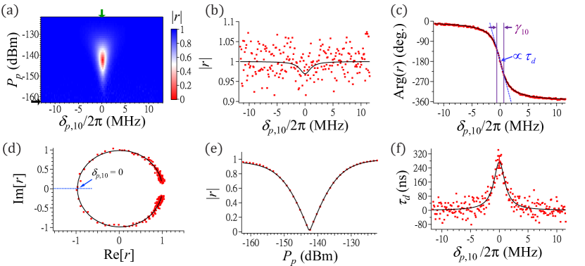
During the calibration process for Device 2, we select the lowest power from Fig. S2(a) (black arrow); this line cut is shown in Fig. S2(b). The incident field is here almost fully reflected by the atom, with |r|0.97similar-to-or-equals𝑟0.97|r|\simeq 0.97, which indicates that Ωpγ10much-less-thansubscriptΩ𝑝subscript𝛾10\Omega_{p}\ll\gamma_{10} and Γ10Γ10nmuch-greater-thansubscriptΓ10subscriptsuperscriptΓ𝑛10\Gamma_{10}\gg\Gamma^{n}_{10}. Due to the low signal-to-noise ratio of the weak probe, there is a significant fluctuation in the magnitude of |r|𝑟|r|. However, when mapping r𝑟r in the IQ plane, as shown in Fig. S2(d), this fluctuation has a relatively lesser impact. This enables us to employ a circle-fit method [3, 4], which is less affected by the fluctuations and provides a more robust estimation of the parameters. By fitting the data points on the IQ plane to a circle, we can accurately determine the relevant parameters despite the presence of noise in |r|𝑟|r|. Utilizing this method, we extract the parameters Γ10subscriptΓ10\Gamma_{10} and γ10subscript𝛾10\gamma_{10} using Eq. (S1); the results are summarized in Table S1 together with other extracted parameters.

Device ω10/2πsubscript𝜔102𝜋\omega_{10}/2\pi Γ10/2πsubscriptΓ102𝜋\Gamma_{10}/2\pi γ10/2πsubscript𝛾102𝜋\gamma_{10}/2\pi Γ10n/2πsuperscriptsubscriptΓ10𝑛2𝜋\Gamma_{10}^{n}/2\pi k10subscript𝑘10k_{10} Γ21/2πsubscriptΓ212𝜋\Gamma_{21}/2\pi γ20/2πsubscript𝛾202𝜋\gamma_{20}/2\pi Γ20n/2πsuperscriptsubscriptΓ20𝑛2𝜋\Gamma_{20}^{n}/2\pi
- MHz MHz MHz MHz Hz/WW\sqrt{\text{W}} MHz MHz MHz
1a 7605.7 ±plus-or-minus\pm 0.7 6.96 ±plus-or-minus\pm 0.29 11.8 ±plus-or-minus\pm 0.8 8.3 ±plus-or-minus\pm 0.8 9.37 \cdot 1014superscript101410^{14} - - -
1b 7799.0 ±plus-or-minus\pm 0.4 33.07 ±plus-or-minus\pm 0.28 22.6 ±plus-or-minus\pm 0.4 6.1 ±plus-or-minus\pm 0.4 2.0185 \cdot 1015superscript101510^{15} - - -
2 4761.62 ±plus-or-minus\pm 0.013 2.316 ±plus-or-minus\pm 0.018 1.176 ±plus-or-minus\pm 0.013 0.017 ±plus-or-minus\pm 0.016 6.8363 \cdot 1014superscript101410^{14} 4.632 ±plus-or-minus\pm 0.037 2.364 ±plus-or-minus\pm 0.042 0.048 ±plus-or-minus\pm 0.046
Table S1: Extracted parameters of the artificial atoms in Devices 1 and 2. The Device labels 1a and 1b are used to refer to the typical parameters of Device 1 measured at two different |0|1ket0ket1|0\rangle\leftrightarrow|1\rangle transition frequencies. The label 1a corresponds to measurements taken near the node (the node is at 7534MHz7534MHz7534\,\mathrm{MHz}) and 1b denotes measurements conducted near the antinode (the antinode is at 7982MHz7982MHz7982\,\mathrm{MHz}). The |2|0ket2ket0|2\rangle\leftrightarrow|0\rangle decoherence rate is given by γ20=Γ21/2+Γ20nsubscript𝛾20subscriptΓ212subscriptsuperscriptΓ𝑛20\gamma_{20}=\Gamma_{21}/2+\Gamma^{n}_{20} [5], where Γ21subscriptΓ21\Gamma_{21} and Γ20nsubscriptsuperscriptΓ𝑛20\Gamma^{n}_{20} are the |2|1ket2ket1|2\rangle\rightarrow|1\rangle decay rate and the combined non-radiative decay rate for the |2|0ket2ket0|2\rangle\leftrightarrow|0\rangle transition, respectively. The value of Γ21subscriptΓ21\Gamma_{21} is determined by considering its relation to Γ10subscriptΓ10\Gamma_{10} based on the coupling matrix element, which is twice the value of Γ10subscriptΓ10\Gamma_{10}.

In Fig. S2(e), where the probe is resonant with the atom (δp,10=0subscript𝛿𝑝100\delta_{p,10}=0), we fit the power dependence with Eq. (S1), extract k10subscript𝑘10k_{10} and determine ΩpsubscriptΩ𝑝\Omega_{p} (see Table S1) with corresponding VNA power, thus obtaining the effective attenuation A𝐴A and gain G𝐺G [6]. These calibration steps can be applied to both frequency-domain and time-domain measurements. The extracted data (A𝐴A, G𝐺G) are shown in Table S2. The parameter difference between the time- and frequency-domain setups is from the additional attenuation in the up-converting IQ modulator and the down-converting mixing in the time-domain setup.

Afreqsubscript𝐴freqA_{\rm freq} Gfreqsubscript𝐺freqG_{\rm freq} Atimesubscript𝐴timeA_{\rm time} Gtimesubscript𝐺timeG_{\rm time}
dB dB dB dB
132.3132.3132.3 60.660.660.6 143.7143.7143.7 101.4101.4101.4
Table S2: Extracted effective attenuations A𝐴A and gains G𝐺G. The subscripts for A𝐴A and G𝐺G represent the time-domain and frequency-domain systems, respectively [see Fig. S1(a)]. Details of the calibration method are shown in Ref. [6].

A π𝜋\pi phase shift occurs when the probe is resonant with the atom in Fig. S2(c). It suggests again that the atom-mirror system is in the strong coupling regime, where the coherent coupling Γ10subscriptΓ10\Gamma_{10} is much larger that any loss or pure dephasing in the system, i.e., γ10Γ10/2similar-to-or-equalssubscript𝛾10subscriptΓ102\gamma_{10}\simeq\Gamma_{10}/2. Even in the strong coupling regime, we maintain a narrow linewidth of γ10/2π1MHzsimilar-to-or-equalssubscript𝛾102𝜋1MHz\gamma_{10}/2\pi\simeq 1\,\mathrm{MHz}. Consequently, there is a steep slope in the phase response, as shown in the blue curve in Fig. S2(c). The slope is directly linked to the group delay time τdsubscript𝜏𝑑\tau_{d}, according to Ref. [7]:

τd=Arg(r)ωp,subscript𝜏𝑑Arg𝑟subscript𝜔𝑝\tau_{d}=-\frac{\partial\mathrm{Arg}(r)}{\partial\omega_{p}}, (S4)

where Arg(r)Arg𝑟\mathrm{Arg}(r) is the phase of the complex reflection coefficient. The calculated τdsubscript𝜏𝑑\tau_{d} from Fig. S2(c), according to Eq. (S4), is presented in Fig. S2(f) and provides a prediction of τdsubscript𝜏𝑑\tau_{d} prior to the time-domain measurement. The predicted maximum τdsubscript𝜏𝑑\tau_{d} is approximately 274ns274ns274\,\mathrm{ns}. Further details of the derivation of τdsubscript𝜏𝑑\tau_{d} are presented in Sec. S7.

We perform the same measurements to characterize Device 1; some of the results are shown in Fig. S3. The diameter of the resonant circle, given by Γ10/γ10subscriptΓ10subscript𝛾10\Gamma_{10}/\gamma_{10}, decreases as ω10/2πsubscript𝜔102𝜋\omega_{10}/2\pi approaches to the node frequency in Fig. S3(a). This decrease indicates that the coupling is reduced. We perform time-domain measurements in the subsequent sections.

Refer to caption
Figure S3: Characterization of Device 1: In (a) and (b), the black curves represent theoretical fittings based on Eq. (S1). The colored dots are the measured data points with the atom bias set at ω10/2πsubscript𝜔102𝜋\omega_{10}/2\pi of 7.6057GHz7.6057GHz7.6057\,\mathrm{GHz} (orange) and 7.799GHz7.799GHz7.799\,\mathrm{GHz} (red), respectively. (a) The reflection coefficient plotted in the IQ plane for a weak probe at Ωp/2π=0.64MHzsubscriptΩ𝑝2𝜋0.64MHz\Omega_{p}/2\pi=0.64\,\mathrm{MHz} (orange) and 1.29MHz1.29MHz1.29\,\mathrm{MHz} (red). (b) The on-resonance |r|𝑟|r| as a function of power for the two values of ω10/2πsubscript𝜔102𝜋\omega_{10}/2\pi. (c) The extracted Γ10/2πsubscriptΓ102𝜋\Gamma_{10}/2\pi (red), γ10/2πsubscript𝛾102𝜋\gamma_{10}/2\pi (orange), and Γ10n/2πsubscriptsuperscriptΓ𝑛102𝜋\Gamma^{n}_{10}/2\pi (green) when the atom is biased at different ω10/2πsubscript𝜔102𝜋\omega_{10}/2\pi. All three rates shift slightly between two cooldowns. The panels (a)–(b) and the spectroscopic data in Fig. 2(a)–(e) in the main text correspond to the parameters obtained from the first cooldown (represented by circles), while the time-domain-related results in Fig. 2(e)–(f) are associated with the qubit parameters obtained from the second cooldown (represented by triangles). The red arrow indicates Γ10/2=Γ10nsubscriptΓ102subscriptsuperscriptΓ𝑛10\Gamma_{10}/2=\Gamma^{n}_{10}, where a singularity occurs for the group delay time. This separates regions of negative group delay (τd<0subscript𝜏𝑑0\tau_{d}<0) and positive group delay region (τd>0subscript𝜏𝑑0\tau_{d}>0). It is important to note that the frequency of the singularity remains nearly the same between the two cooldowns.

S3 Group delay time as a function of pulse width

We send a weak (162.3dBm162.3dBm-162.3\,\mathrm{dBm}) probing Gaussian pulse with a variable pulse width σ𝜎\sigma to the atom-mirror system (Device 2). The dependence of the group delay time τdsubscript𝜏𝑑\tau_{d} on the probe power is discussed in Sec. S5. The carrier frequency of the probe is provided by an RF source, and the amplitude modulation signal is produced by the AWG (see Fig. S1).

Refer to caption
Figure S4: Sending Gaussian pulses (with a time resolution of 1ns1ns1\,\mathrm{ns}) to the atom-mirror system for Device 2. Pulse envelope changes of the output signals are displayed for three different pulse widths σ𝜎\sigma: (a) 105ns105ns105\,\mathrm{ns}, (b) 728ns728ns728\,\mathrm{ns}, and (c) 1040ns1040ns1040\,\mathrm{ns}. Experimental data are shown in red dots (with the atom) and green dots (without the atom, which then is far detuned). The orange curves are based on Gaussian fitting, and the black curves are based on optical Bloch equations and the input-output relation [8] with the parameters of Device 2 in Table S1. The theory curves maintain good agreement with the experimental data to extract τdsubscript𝜏𝑑\tau_{d}: (a) τd=159nssubscript𝜏𝑑159ns\tau_{d}=159\,\mathrm{ns}, (b) τd=269nssubscript𝜏𝑑269ns\tau_{d}=269\,\mathrm{ns}, and (c) τd=273nssubscript𝜏𝑑273ns\tau_{d}=273\,\mathrm{ns}. (d) Summary of τdsubscript𝜏𝑑\tau_{d} as a function of σ𝜎\sigma when the pulse is resonant with the atom. The red dots are measured data and the dashed curve is the simulated prediction.

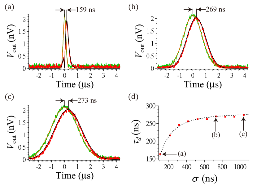
The theoretical simulation procedure is as follows: first, a Gaussian function is employed to fit the reference Gaussian pulse measured when the atom is far-detuned. The parameters obtained from the fitted Gaussian pulse, represented by the orange curves in Fig. S4, are then combined with the parameters given in Table S1. Subsequently, the evolution of the output pulses is simulated using optical Bloch equations and the input-output relation [8]. The simulated results of the output pulse are depicted as the black solid curves in Fig. S4. Finally, τdsubscript𝜏𝑑\tau_{d} is calculated as the time difference between the two peaks.

As depicted in Fig. S4, the simulation curves exhibit good agreement with the experimental data (red dots). As the value of σ𝜎\sigma increases, τdsubscript𝜏𝑑\tau_{d} increases. The larger σ𝜎\sigma indicates a narrower signal bandwidth distribution in frequency domain. When σ𝜎\sigma is 1040ns1040ns1040\,\mathrm{ns} [see Fig. S4(c)], τdsubscript𝜏𝑑\tau_{d} reaches up to 273 ns. In this scenario, the bandwidth of the incoming field (1MHzsimilar-to-or-equalsabsent1MHz\simeq 1\,\mathrm{MHz}) lies within the linewidth of the artificial atom (γ102π×1.2MHzsimilar-to-or-equalssubscript𝛾102𝜋1.2MHz\gamma_{10}\simeq 2\pi\times 1.2\,\mathrm{MHz}). Consequently, the incoming field resides in the linear dispersive region, where all the spectral components are subject to the same group delay.

In the case where σ𝜎\sigma is 105ns105ns105\,\mathrm{ns} [see Fig. S4(a)], two distinct sharp peaks emerge in the output. This phenomenon occurs because the signal bandwidth (10MHzsimilar-to-or-equalsabsent10MHz\simeq 10\,\mathrm{MHz}) for σ=105ns𝜎105ns\sigma=105\,\mathrm{ns} is wider than the linewidth of the atom (γ10subscript𝛾10\gamma_{10}). Consequently, the output signal experiences distortions caused by the non-homogeneous reflection magnitude and group delay. The interference between the input wave and the atom emission, characterized by opposite phases, gives rise to the observed double sharp peaks.

S4 Group delay time as a function of probe-frequency detuning

Refer to caption
Figure S5: Pulse-envelope dependence on the probe frequency of weak Gaussian pulses with σ1μssimilar-to-or-equals𝜎1μs\sigma\simeq 1\,\mathrm{\upmu s}. The probe frequency of the Gaussian pulse is detuned away from the atom by δp,10/2πsubscript𝛿𝑝102𝜋\delta_{p,10}/2\pi = (a) 5MHz5MHz-5\,\mathrm{MHz}, (b) 1MHz1MHz-1\,\mathrm{MHz}, and (c) 0MHz0MHz0\,\mathrm{MHz}. Experimental data are shown as red dots (with the atom) and green dots (without the atom, which then is far detuned). The orange curves are based on Gaussian fitting, and the black curves are based on optical Bloch equations and the input-output relation [8] with the parameters of Device 2 in Table S1. The extracted τdsubscript𝜏𝑑\tau_{d} is (a) 15 ns, (b) 161 ns, and (c) 271 ns. (d) Summary of extracted τdsubscript𝜏𝑑\tau_{d} as a function of δp,10/2πsubscript𝛿𝑝102𝜋\delta_{p,10}/2\pi. The red dots are extracted data and the dashed curve is a simulation.

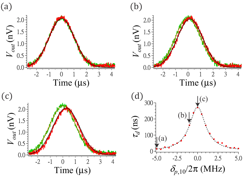
In this section, for Device 2 with a fixed ω10=4761.62MHzsubscript𝜔104761.62MHz\omega_{10}=4761.62\,\mathrm{MHz}, the probe frequency ωp/2πsubscript𝜔𝑝2𝜋\omega_{p}/2\pi of the Gaussian pulses is swept from ω10/2π5MHzsubscript𝜔102𝜋5MHz\omega_{10}/2\pi-5\,\mathrm{MHz} to ω10/2π+5MHzsubscript𝜔102𝜋5MHz\omega_{10}/2\pi+5\,\mathrm{MHz}, where σ1μssimilar-to-or-equals𝜎1μs\sigma\simeq 1\,\mathrm{\upmu s}. The simulation procedure follows the same steps as described in Sec. S3. In Fig. S5, the simulated black curves show good agreement with the measured data (red dots). The values of the group delay time τdsubscript𝜏𝑑\tau_{d} obtained from the simulation in Fig. S5(d) are consistent with the results from the frequency-domain measurements in Fig. S2(f), but display reduced fluctuations. The maximum τdsubscript𝜏𝑑\tau_{d} occurs when the probe frequency of the Gaussian pulse is on resonance with the atom. This corresponds to the most significant change in phase response, as shown in Fig. S2(c).

In Fig. S5(b), when the detuning δp,10/2π=1MHzsubscript𝛿𝑝102𝜋1MHz\delta_{p,10}/2\pi=-1\,\mathrm{MHz}, τdsubscript𝜏𝑑\tau_{d} decreases from its maximum 271 ns (on resonance, δp,10=0subscript𝛿𝑝100\delta_{p,10}=0) to 161 ns. In Fig. S5(a), where the detuning is increased to δp,10/2π=5MHzsubscript𝛿𝑝102𝜋5MHz\delta_{p,10}/2\pi=-5\,\mathrm{MHz}, τdsubscript𝜏𝑑\tau_{d} decreases further to 15 ns. Therefore, by detuning the probe frequency of the Gaussian pulses, we can adjust τdsubscript𝜏𝑑\tau_{d} in the range of 0 to 271 ns to control the effect of positive group delay. This approach complements two methods presented in the main text, enhancing our ability to manipulate the group delay of the light.

S5 Pulse-envelope evolution as a function of probe power

Refer to caption
Figure S6: Pulse-envelope variation for different probe powers (Ppsubscript𝑃𝑝P_{p}) of the Gaussian pulse with σ1μssimilar-to-or-equals𝜎1μs\sigma\simeq 1\,\mathrm{\upmu s}: (a) 147.7dBm147.7dBm-147.7\,\mathrm{dBm}, (b) 141.7dBm141.7dBm-141.7\,\mathrm{dBm}, (c) 137.7dBm137.7dBm-137.7\,\mathrm{dBm}, and (d) 123.7dBm123.7dBm-123.7\,\mathrm{dBm}. Experimental data are shown in red dashed curves (with the atom) and green dashed curves (without the atom, which then is far detuned). The orange curves are based on Gaussian fitting and the black curves are based on optical Bloch equations and the input-output relation [8] with the parameters of Device 2 in Table S1.

In this section, we investigate the behavior of Device 2 by sending Gaussian pulses with different probe powers, while keeping the detuning δp,10=0subscript𝛿𝑝100\delta_{p,10}=0 and the pulse width σ1μssimilar-to-or-equals𝜎1μs\sigma\simeq 1\,\mathrm{\upmu s} constant. As discussed in Sec. S3, for this pulse width the bandwidth of the incoming Gaussian pulses (1MHzsimilar-to-or-equalsabsent1MHz\simeq 1\,\mathrm{MHz}) falls within the linewidth of the artificial atom (γ10subscript𝛾10\gamma_{10}). Hence, in the time domain, where σ1μssimilar-to-or-equals𝜎1μs\sigma\simeq 1\,\mathrm{\upmu s} is much larger than the atom’s response time T2=1/γ10135nssubscript𝑇21subscript𝛾10similar-to-or-equals135nsT_{2}=1/\gamma_{10}\simeq 135\,\mathrm{ns}, the atom sees the input approximately as a continuous wave. With this approximation, we can estimate the output response by utilizing the reflection coefficient given in Eq. (S1). In Fig. S6, we observe that the time-domain results indeed exhibit the same trend as the power dependence of |r|𝑟|r| at δp,10=0subscript𝛿𝑝100\delta_{p,10}=0 shown in Fig. S2(e).

The cases depicted in Fig. S6 can be divided into two regions based on the input voltage of 24.3nV24.3nV24.3\,\mathrm{nV}, which corresponds to the singularity point |r|=0𝑟0|r|=0 at Pp=142.3dBmsubscript𝑃𝑝142.3dBmP_{p}=-142.3\,\mathrm{dBm} in Fig. S2(e). The input voltage is equivalent to the far-detuned curves in Fig. S6 (orange curves). In Fig. S6(a), when the peak input voltage is smaller than 24.3 nV, the input pulse undergoes distortion in both magnitude and phase due to the power dependence of r𝑟r.

As depicted in Fig. S6(b)–(d), when the peak input voltage exceeds 24.3 nV, indicated by horizontal lines, the amplitude around the peak corresponds to Re[r]>0Redelimited-[]𝑟0\text{Re}{[r]}>0. When the input voltage <24.3nVabsent24.3nV<24.3\,\mathrm{nV}, the other amplitude corresponds to Re[r]<0Redelimited-[]𝑟0\text{Re}{[r]}<0. This leads to the emergence of two dips in the output waveform, indicating that the input amplitudes have reached the singularity point. Moreover, with a further increase in the probe power, the atom becomes saturated, causing the output waveform to approach the input waveform, corresponding to r𝑟r reaching unity.

S6 Autler–Townes splitting as a function of control power

Refer to caption
Figure S7: (a) Dressed 3-level system diagram showing the Autler–Townes splitting. A strong control tone dresses the |1|2ket1ket2|1\rangle\leftrightarrow|2\rangle transition of the artificial atom, splitting the levels |1ket1|1\rangle and |2ket2|2\rangle individually into dressed states with a splitting of ΩcsubscriptΩ𝑐\Omega_{c} for each. (b) Theoretical simulation of |r|𝑟|r| [corresponds Fig. 3(a) in the main text], illustrating the Autler–Townes splitting of the artificial atom, based on Eq. (S5) with the parameters in Table S1 for Device 2. (c) The theoretical group delay time τdsubscript𝜏𝑑\tau_{d} [corresponds to Fig. 3(b) in the main text] as a function of δp,10subscript𝛿𝑝10\delta_{p,10} and Pcsubscript𝑃𝑐P_{c}. When δp,10=0subscript𝛿𝑝100\delta_{p,10}=0, the theoretical τdsubscript𝜏𝑑\tau_{d} along the dashed line corresponds to the solid deep blue curve in Fig. 3(e) in the main text. (d) Measured Voutsubscript𝑉outV_{\rm out} of the Gaussian-pulse (σ1μssimilar-to-or-equals𝜎1μs\sigma\simeq 1\,\mathrm{\upmu s}) probe field as a function of time and the control-tone power Pcsubscript𝑃𝑐P_{c}. The extracted τdsubscript𝜏𝑑\tau_{d} corresponds to the pink data points in Fig. 3(e) in the main text. (e) The corresponding theoretical prediction for (d) is simulated based on Eqs. (S6)–(S8) and the input-output relation [8] with the parameters in Table S1 for Device 2. The arrows in (d) and (e) indicate line cuts in Fig. 3(f) in the main text.

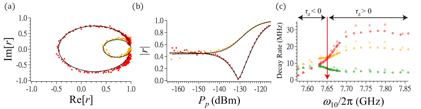
In this section, we employ two-tone spectroscopy to investigate our system in Device 2. On top of the sweeping weak probe tone (approximately 162.3dBm162.3dBm-162.3\,\mathrm{dBm}), we apply a control tone that is resonant with the |1|2ket1ket2|1\rangle\leftrightarrow|2\rangle transition of the atom. By utilizing the Autler–Townes splitting (ATS) effect depicted in Fig. S7(a), we demonstrate effective switching on and off of the group delay of the light. This allows us to explore fine-tuning the system from positive to negative group delay for the light. In Fig. S7(b), as the power of the control tone (Pcsubscript𝑃𝑐P_{c}) increases, the |0|1ket0ket1|0\rangle\leftrightarrow|1\rangle transition gradually splits into two transitions from the ground state to dressed states due to ATS.

The reflection coefficient for the weak probe in this case is given by [2]

r=12Γ102(γ10+iδp,10)+Ωc2/[2γ20+2i(δp,10+δc,21)],𝑟12subscriptΓ102subscript𝛾10𝑖subscript𝛿𝑝10superscriptsubscriptΩ𝑐2delimited-[]2subscript𝛾202𝑖subscript𝛿𝑝10subscript𝛿𝑐21r=1-\frac{2\Gamma_{10}}{2\left(\gamma_{10}+i\delta_{p,10}\right)+\Omega_{c}^{2}/\left[2\gamma_{20}+2i\left(\delta_{p,10}+\delta_{c,21}\right)\right]}, (S5)

were δc,21=ωcω21subscript𝛿𝑐21subscript𝜔𝑐subscript𝜔21\delta_{c,21}=\omega_{c}-\omega_{21} is the detuning of the control-tone frequency ωcsubscript𝜔𝑐\omega_{c} from the |1|2ket1ket2|1\rangle\leftrightarrow|2\rangle transition frequency ω21subscript𝜔21\omega_{21} and the Rabi frequency Ωc=k21PcsubscriptΩ𝑐subscript𝑘21subscript𝑃𝑐\Omega_{c}=k_{21}\sqrt{P_{c}} of the control tone is proportional to the square root of the control-tone power. We can extract γ20subscript𝛾20\gamma_{20} from experimental data [Fig. 3(a) in the main text] using Eq. (S5), utilizing the parameters γ10subscript𝛾10\gamma_{10}, Γ10subscriptΓ10\Gamma_{10}, and k10subscript𝑘10k_{10}) from Table S1 (Device 2), and the coupling-constant relationship between k21subscript𝑘21k_{21} and k10subscript𝑘10k_{10}. Given that Γ21subscriptΓ21\Gamma_{21} is estimated to be twice Γ10subscriptΓ10\Gamma_{10} [1], and k10subscript𝑘10k_{10} is proportional to the square root of Γ10subscriptΓ10\Gamma_{10} [6], we can approximate k212k10similar-to-or-equalssubscript𝑘212subscript𝑘10k_{21}\simeq\sqrt{2}k_{10}. The value of γ20subscript𝛾20\gamma_{20} is listed in Table S1. Consequently, we plot the theoretical ATS spectrum based on Eq. (S5), illustrated in Fig. S7(b). All the fitting is performed without any free parameters. The results demonstrate excellent agreement between theoretical simulations and experimental results.

In the time domain, we send Gaussian pulses with σ1μssimilar-to-or-equals𝜎1μs\sigma\simeq 1\,\mathrm{\upmu s} to the system, while simultaneously applying a continuous control tone with varying power levels. The output Gaussian pulses for different control power levels are shown in Fig. S7(d), which matches well with simulation results in Fig. S7(e). Notably, the negative-group-delay light is observed in the power range of 139.24dBm139.24dBm-139.24\,\mathrm{dBm} to 136.21dBm136.21dBm-136.21\,\mathrm{dBm}, as shown in Fig. 3(e) in the main text.

For the simulations in the time domain, we assume that the atom starts in its ground state. The time evolution of the elements of the density matrix for the three-level atom is then given by [2]

tρ10subscript𝑡subscript𝜌10\displaystyle\partial_{t}\rho_{10} =(iδp,10γ10)ρ10+i2Ωc(t)ρ20+i2Ωp(t)ρ00,absent𝑖subscript𝛿𝑝10subscript𝛾10subscript𝜌10𝑖2subscriptΩ𝑐𝑡subscript𝜌20𝑖2subscriptΩ𝑝𝑡subscript𝜌00\displaystyle=\left(-i\delta_{p,10}-\gamma_{10}\right)\rho_{10}+\frac{i}{2}\Omega_{c}(t)\rho_{20}+\frac{i}{2}\Omega_{p}(t)\rho_{00}, (S6)
tρ20subscript𝑡subscript𝜌20\displaystyle\partial_{t}\rho_{20} =i2Ωc(t)ρ10[i(δp,10+δc,21)+γ20]ρ20i2Ωp(t)ρ21,absent𝑖2subscriptΩ𝑐𝑡subscript𝜌10delimited-[]𝑖subscript𝛿𝑝10subscript𝛿𝑐21subscript𝛾20subscript𝜌20𝑖2subscriptΩ𝑝𝑡subscript𝜌21\displaystyle=\frac{i}{2}\Omega_{c}(t)\rho_{10}-\left[i\left(\delta_{p,10}+\delta_{c,21}\right)+\gamma_{20}\right]\rho_{20}-\frac{i}{2}\Omega_{p}(t)\rho_{21}, (S7)
tρ21subscript𝑡subscript𝜌21\displaystyle\partial_{t}\rho_{21} =i2Ωp(t)ρ20(iδc,21+γ21)ρ21.absent𝑖2subscriptΩ𝑝𝑡subscript𝜌20𝑖subscript𝛿𝑐21subscript𝛾21subscript𝜌21\displaystyle=-\frac{i}{2}\Omega_{p}(t)\rho_{20}-\left(i\delta_{c,21}+\gamma_{21}\right)\rho_{21}. (S8)

Combined with the input-output relation [8], the positive- and negative-group-delay time dynamics of the output response can be numerically solved, as shown in Fig. S7(e).

S7 Group delay and reflection coefficient in the weakly probed atom-waveguide system

In this section, we begin by deriving the output response of the atom-mirror system in the frequency domain for a given input signal. Then, we use the narrowband property of our input signal to simplify the output expression and derive the expression for the group delay time utilized in this work.

An artificial atom is typically a nonlinear system characterized by its power dependence. The emission of the artificial atom is determined by its state, which naturally decays over time, resulting in a time-variant system. To use the atom as a filter in our work, we consider the following schemes: firstly, by utilizing the weak probe, the system experiences a weak excitation. This results in the atom predominantly remaining in its ground state and linearizes the system response. Secondly, the use of a dilution refrigerator helps to maintain the system in a stable ground state with negligible thermal fluctuations until the input probe pulse arrives. Under these conditions, the system remains linear and time-invariant throughout the entire duration of the experiment.

Based on the power dependence of the spectroscopy Fig. S2(e), we know that the atom exhibits a linear response at low probe power. To analyze this linear region, we apply perturbation theory [9] to derive an analytical solution. Specifically, the small parameter used for determining the order of perturbation is Ωp/γ10subscriptΩ𝑝subscript𝛾10\Omega_{p}/\gamma_{10}. We expand the system density matrix to the first order:

ρ^(t)=ρ^(0)(t)+ρ^(1)(t).^𝜌𝑡superscript^𝜌0𝑡superscript^𝜌1𝑡\hat{\rho}(t)=\hat{\rho}^{(0)}(t)+\hat{\rho}^{(1)}(t). (S9)

Thorough this section, the superscript indicates the order of perturbation.

We consider a three-level Hamiltonian with corresponding dissipator [10]

H^=2(0Ωp(t)0Ωp(t)2δp,10Ωc0Ωc2(δp,10+δc,21)),^𝐻Planck-constant-over-2-pi2matrix0subscriptΩ𝑝𝑡0subscriptΩ𝑝𝑡2subscript𝛿𝑝10subscriptΩ𝑐0subscriptΩ𝑐2subscript𝛿𝑝10subscript𝛿𝑐21\displaystyle\hat{H}=\frac{\hbar}{2}\begin{pmatrix}0&\Omega_{p}(t)&0\\ \Omega_{p}(t)&-2\delta_{p,10}&\Omega_{c}\\ 0&\Omega_{c}&-2\left(\delta_{p,10}+\delta_{c,21}\right)\\ \end{pmatrix}, (S10)
[ρ^]=(Γ10ρ11γ10ρ01γ20ρ02γ10ρ10Γ21ρ22Γ10ρ11γ21ρ12γ20ρ20γ21ρ21Γ21ρ22).delimited-[]^𝜌matrixsubscriptΓ10subscript𝜌11subscript𝛾10subscript𝜌01subscript𝛾20subscript𝜌02subscript𝛾10subscript𝜌10subscriptΓ21subscript𝜌22subscriptΓ10subscript𝜌11subscript𝛾21subscript𝜌12subscript𝛾20subscript𝜌20subscript𝛾21subscript𝜌21subscriptΓ21subscript𝜌22\displaystyle\mathcal{L}\left[\hat{\rho}\right]=\begin{pmatrix}\Gamma_{10}\rho_{11}&-\gamma_{10}\rho_{01}&-\gamma_{20}\rho_{02}\\ -\gamma_{10}\rho_{10}&\Gamma_{21}\rho_{22}-\Gamma_{10}\rho_{11}&-\gamma_{21}\rho_{12}\\ -\gamma_{20}\rho_{20}&-\gamma_{21}\rho_{21}&-\Gamma_{21}\rho_{22}\\ \end{pmatrix}. (S11)

We then solve the master equation

dρ^dt=i[ρ^,H^]+[ρ^].𝑑^𝜌𝑑𝑡𝑖Planck-constant-over-2-pi^𝜌^𝐻delimited-[]^𝜌\frac{d\hat{\rho}}{dt}=-\frac{i}{\hbar}\left[\hat{\rho},\hat{H}\right]+\mathcal{L}\left[\hat{\rho}\right]. (S12)

by employing the Laplace transform with the initial condition that the atom is in its ground state. Iteratively solving each order of perturbation, we acquire the first-order expansion, which is expressed as

ρ^(s)=(1ρ10(1)(s)ρ20(1)(s)ρ10(1)(s)00ρ20(1)(s)00),^𝜌𝑠matrix1superscriptsubscript𝜌101superscript𝑠superscriptsubscript𝜌201superscript𝑠superscriptsubscript𝜌101𝑠00superscriptsubscript𝜌201𝑠00\hat{\rho}(s)=\begin{pmatrix}1&\rho_{10}^{(1)}(s)^{*}&\rho_{20}^{(1)}(s)^{*}\\ \rho_{10}^{(1)}(s)&0&0\\ \rho_{20}^{(1)}(s)&0&0\\ \end{pmatrix}, (S13)

where

ρ10(1)(s)=i2Ωp(s)s+i(δp,10+δc,21)+γ20(s+iδp,10+γ10)[s+i(δp,10+δc,21)+γ20]+Ωc24,superscriptsubscript𝜌101𝑠𝑖2subscriptΩ𝑝𝑠𝑠𝑖subscript𝛿𝑝10subscript𝛿𝑐21subscript𝛾20𝑠𝑖subscript𝛿𝑝10subscript𝛾10delimited-[]𝑠𝑖subscript𝛿𝑝10subscript𝛿𝑐21subscript𝛾20superscriptsubscriptΩ𝑐24\displaystyle\rho_{10}^{(1)}(s)=\frac{i}{2}\Omega_{p}(s)\frac{s+i\left(\delta_{p,10}+\delta_{c,21}\right)+\gamma_{20}}{\left(s+i\delta_{p,10}+\gamma_{10}\right)\left[s+i\left(\delta_{p,10}+\delta_{c,21}\right)+\gamma_{20}\right]+\frac{\Omega_{c}^{2}}{4}}, (S14)
ρ20(1)(s)=i2Ωp(s)iΩc/2(s+iδp,10+γ10)[s+i(δp,10+δc,21)+γ20]+Ωc24.superscriptsubscript𝜌201𝑠𝑖2subscriptΩ𝑝𝑠𝑖subscriptΩ𝑐2𝑠𝑖subscript𝛿𝑝10subscript𝛾10delimited-[]𝑠𝑖subscript𝛿𝑝10subscript𝛿𝑐21subscript𝛾20superscriptsubscriptΩ𝑐24\displaystyle\rho_{20}^{(1)}(s)=\frac{i}{2}\Omega_{p}(s)\frac{i\Omega_{c}/2}{\left(s+i\delta_{p,10}+\gamma_{10}\right)\left[s+i\left(\delta_{p,10}+\delta_{c,21}\right)+\gamma_{20}\right]+\frac{\Omega_{c}^{2}}{4}}. (S15)

Here, we denote by f(s)={f(t)}𝑓𝑠𝑓𝑡f(s)=\mathscr{L}\{f(t)\} the Laplace transform of a time-varying function f(t)𝑓𝑡f(t) throughout this section. Further investigation of the second-order expansion allows us to obtain non-zero corrections for coherence and population. The first-order expansion allows us to approximate the atom to be predominantly in its ground state, exhibiting time invariance.

The input-output relation for the probe tone [8] after Laplace transformation can be expressed as

Ωout(s)=Ωp(s)+2iΓ10ρ10(s),subscriptΩout𝑠subscriptΩ𝑝𝑠2𝑖subscriptΓ10subscript𝜌10𝑠\Omega_{\rm out}(s)=\Omega_{p}(s)+2i\Gamma_{10}\rho_{10}(s), (S16)

where ΩoutsubscriptΩout\Omega_{\rm out} is the coherent output voltage in Rabi-frequency scale. Plugging Eq. (S14) into Eq. (S16), we obtain the transfer function

T(s)=Ωout(s)Ωp(s)=1Γ10s+iδp,10+γ10+Ωc24[s+i(δp,10+δc,21)+γ20].𝑇𝑠subscriptΩout𝑠subscriptΩ𝑝𝑠1subscriptΓ10𝑠𝑖subscript𝛿𝑝10subscript𝛾10superscriptsubscriptΩ𝑐24delimited-[]𝑠𝑖subscript𝛿𝑝10subscript𝛿𝑐21subscript𝛾20\begin{split}T(s)=\frac{\Omega_{\rm out}(s)}{\Omega_{p}(s)}=1-\frac{\Gamma_{10}}{s+i\delta_{p,10}+\gamma_{10}+\frac{\Omega_{c}^{2}}{4\left[s+i\left(\delta_{p,10}+\delta_{c,21}\right)+\gamma_{20}\right]}}.\end{split} (S17)

The independence of Eq. (S17) from Ωp(t)subscriptΩ𝑝𝑡\Omega_{p}(t) shows the linearity of the system. Here we assign s=iωe𝑠𝑖subscript𝜔𝑒s=i\omega_{e} to investigate the frequency response, where ωesubscript𝜔𝑒\omega_{e} represents the relative distance from the carrier frequency ωpsubscript𝜔𝑝\omega_{p}. The reflection coefficient r𝑟r used in the spectroscopy, obtained from solving the steady-state solution of Eq. (S12) as Ωp(t)=Ωpγ10subscriptΩ𝑝𝑡subscriptΩ𝑝much-less-thansubscript𝛾10\Omega_{p}(t)=\Omega_{p}\ll\gamma_{10}, corresponds to the case r=T(0)𝑟𝑇0r=T(0) and is given in Eq. (S5).

Given an input pulse Ωp(t)=Ωpexp[(tt0)2/(2σ2)]subscriptΩ𝑝𝑡subscriptΩ𝑝superscript𝑡subscript𝑡022superscript𝜎2\Omega_{p}(t)=\Omega_{p}\exp\left[-\left(t-t_{0}\right)^{2}/\left(2\sigma^{2}\right)\right], where the pulse arrival time t0subscript𝑡0t_{0} is much later than the origin t=0𝑡0t=0 (i.e., t0σmuch-greater-thansubscript𝑡0𝜎t_{0}\gg\sigma), we can neglect the truncation effect in Ωp(s)subscriptΩ𝑝𝑠\Omega_{p}(s). This approximation allows us to treat Ωp(s)subscriptΩ𝑝𝑠\Omega_{p}(s) as the Fourier transform of Ωp(t)subscriptΩ𝑝𝑡\Omega_{p}(t), which is also a Gaussian. The spectral width of Ωp(s)subscriptΩ𝑝𝑠\Omega_{p}(s), which is σ1superscript𝜎1\sigma^{-1} for a Gaussian pulse, is assumed to be much narrower than both the carrier frequency ωpsubscript𝜔𝑝\omega_{p} and the atom linewidth γ10subscript𝛾10\gamma_{10}. Under this assumption, the entire envelope can be approximated as evolving with the nominal carrier frequency ωpsubscript𝜔𝑝\omega_{p}, which corresponds to δp,10=ωpω10subscript𝛿𝑝10subscript𝜔𝑝subscript𝜔10\delta_{p,10}=\omega_{p}-\omega_{10} in Eq. (S5).

Inside Ωp(s)subscriptΩ𝑝𝑠\Omega_{p}(s), the phase of each spectral component of the envelope is given by Arg({Ωp(t)})(ωe)=ωet+ϕωeArgsubscriptΩ𝑝𝑡subscript𝜔𝑒subscript𝜔𝑒𝑡subscriptitalic-ϕsubscript𝜔𝑒\mathrm{Arg}(\mathscr{L}\{\Omega_{p}(t)\})(\omega_{e})=\omega_{e}t+\phi_{\omega_{e}}, where ϕωesubscriptitalic-ϕsubscript𝜔𝑒\phi_{\omega_{e}} is a constant in time and ωesubscript𝜔𝑒\omega_{e} denotes the frequency of the envelope spectral component. This phase is subject to a phase shift

Arg(T)(ωe)Arg(T)(0)+ωeArg(T)ωe|s=0.Arg𝑇subscript𝜔𝑒Arg𝑇0evaluated-atsubscript𝜔𝑒Arg𝑇subscript𝜔𝑒𝑠0\mathrm{Arg}(T)(\omega_{e})\approx\mathrm{Arg}(T)(0)+\omega_{e}\left.\frac{\partial\mathrm{Arg}(T)}{\partial\omega_{e}}\right|_{s=0}. (S18)

Defining the group delay [11]

τd=Arg(T)ωe,subscript𝜏𝑑Arg𝑇subscript𝜔𝑒\tau_{d}=-\frac{\partial\mathrm{Arg}(T)}{\partial\omega_{e}}, (S19)

we see that the negative sign in Eq. (S19) leads to a positive τdsubscript𝜏𝑑\tau_{d} when the slope in Eq. (S18) is negative. Using Eqs. (S17)–(S19), the output phase is

Arg({Ωout(t)})(ωe)=Arg(T)(ωe)+Arg({Ωp(t)})(ωe)ωe(tτd)+ϕωe+Arg(T)(0)=Arg({Ωp(tτd)})(ωe)+Arg(r).ArgsubscriptΩout𝑡subscript𝜔𝑒Arg𝑇subscript𝜔𝑒ArgsubscriptΩ𝑝𝑡subscript𝜔𝑒subscript𝜔𝑒𝑡subscript𝜏𝑑subscriptitalic-ϕsubscript𝜔𝑒Arg𝑇0ArgsubscriptΩ𝑝𝑡subscript𝜏𝑑subscript𝜔𝑒Arg𝑟\begin{split}\mathrm{Arg}(\mathscr{L}\{\Omega_{\rm out}(t)\})(\omega_{e})&=\mathrm{Arg}(T)(\omega_{e})+\mathrm{Arg}(\mathscr{L}\{\Omega_{p}(t)\})(\omega_{e})\\ &\approx\omega_{e}(t-\tau_{d})+\phi_{\omega_{e}}+\mathrm{Arg}(T)(0)\\ &=\mathrm{Arg}(\mathscr{L}\{\Omega_{p}(t-\tau_{d})\})(\omega_{e})+\mathrm{Arg}(r).\end{split} (S20)

From Eq. (S20) we can see that the output envelope is delayed by a time τgsubscript𝜏𝑔\tau_{g} compared to the input from the phase perspective. Using the change of variable ω=ωe+ωp𝜔subscript𝜔𝑒subscript𝜔𝑝\omega=\omega_{e}+\omega_{p}, we can rewrite Eq. (S19) as

τd=Arg(T(0))ω=Arg(r)ω.subscript𝜏𝑑Arg𝑇0𝜔Arg𝑟𝜔\begin{split}\tau_{d}&=-\frac{\partial\mathrm{Arg}(T(0))}{\partial\omega}\\ &=-\frac{\partial\mathrm{Arg}(r)}{\partial\omega}.\end{split} (S21)

Similarly, for the magnitude dispersion:

|T(iωe)||T(0)|+ωe|T|ωe|s=0=|r|.𝑇𝑖subscript𝜔𝑒𝑇0evaluated-atsubscript𝜔𝑒𝑇subscript𝜔𝑒𝑠0𝑟\begin{split}|T(i\omega_{e})|&\approx|T(0)|+\omega_{e}\left.\frac{\partial|T|}{\partial\omega_{e}}\right|_{s=0}\\ &=|r|.\end{split} (S22)

In Eq. (S22), the expression |T|ωe|s=0=|r|δp,10evaluated-at𝑇subscript𝜔𝑒𝑠0𝑟subscript𝛿𝑝10\left.\frac{\partial|T|}{\partial\omega_{e}}\right|_{s=0}=\frac{\partial|r|}{\partial\delta_{p,10}} is complicated, but we can observe that the slope is zero at δp,10=0subscript𝛿𝑝100\delta_{p,10}=0 from the fitting curve in Fig. S2(b), resulting in the only contribution |T(0)|=|r|𝑇0𝑟|T(0)|=|r|. When δp,100subscript𝛿𝑝100\delta_{p,10}\neq 0, the magnitude error can be minimized by selecting a larger σ𝜎\sigma, which has a narrower spectrum width, as shown by the results in Sec. S3.

Summarizing from Eq. (S20) to Eq. (S22), the output response is

Ωout(t)=1{T(s){Ωp(t)}}1{r{Ωp(tτd)}}=r1{{Ωp(tτd)}}=rΩp(tτd).subscriptΩout𝑡superscript1𝑇𝑠subscriptΩ𝑝𝑡superscript1𝑟subscriptΩ𝑝𝑡subscript𝜏𝑑𝑟superscript1subscriptΩ𝑝𝑡subscript𝜏𝑑𝑟subscriptΩ𝑝𝑡subscript𝜏𝑑\begin{split}\Omega_{\rm out}(t)&=\mathscr{L}^{-1}\{T(s)\mathscr{L}\{\Omega_{p}(t)\}\}\\ &\approx\mathscr{L}^{-1}\{r\mathscr{L}\{\Omega_{p}(t-\tau_{d})\}\}\\ &=r\mathscr{L}^{-1}\{\mathscr{L}\{\Omega_{p}(t-\tau_{d})\}\}\\ &=r\Omega_{p}(t-\tau_{d}).\end{split} (S23)

Based on Eq. (S23), the output corresponds to the delayed/advanced version of the input and is additionally rescaled by r𝑟r, given that the spectral content of the envelope is concentrated near the carrier frequency. This provides a straightforward interpretation of our time-domain results and establishes a direct connection to the spectroscopy results. Furthermore, this interpretation holds true for our weakly probed two- or three-level systems because the phenomenon of positive/negative group delay for light is a fundamental characteristic of linear systems. The expressions provided in Eqs. (S21) and (S23) are used in Eq. (2) and Fig. 1 of the main text, respectively.

S8 Deriving effective two-level system reflection coefficient for Device 2

In this section, we derive the effective reflection coefficient of our three-level-atom case for Device 2. Starting from Eq. (S5), we make a Taylor expansion of the denominator in Eq. (S5) near δp,10=0subscript𝛿𝑝100\delta_{p,10}=0, with δp,10/γ101much-less-thansubscript𝛿𝑝10subscript𝛾101\delta_{p,10}/\gamma_{10}\ll 1 the small parameter (δp,10/γ20subscript𝛿𝑝10subscript𝛾20\delta_{p,10}/\gamma_{20} is also small because γ20>γ10subscript𝛾20subscript𝛾10\gamma_{20}>\gamma_{10}). Equation (S5) can then be expanded to

r1Γ101(Ωc2γ20)21γ101+Ωc24γ10γ201(Ωc2γ20)2+iδp,10.𝑟1subscriptΓ101superscriptsubscriptΩ𝑐2subscript𝛾2021subscript𝛾101superscriptsubscriptΩ𝑐24subscript𝛾10subscript𝛾201superscriptsubscriptΩ𝑐2subscript𝛾202𝑖subscript𝛿𝑝10r\approx 1-\frac{\Gamma_{10}}{1-\left(\frac{\Omega_{c}}{2\gamma_{20}}\right)^{2}}\frac{1}{\gamma_{10}\frac{1+\frac{\Omega_{c}^{2}}{4\gamma_{10}\gamma_{20}}}{1-\left(\frac{\Omega_{c}}{2\gamma_{20}}\right)^{2}}+i\delta_{p,10}}. (S24)

By direct comparison to the reflection coefficient for the case of the two-level system, we define the effective rates

ΓΓ\displaystyle\Gamma =Γ101(Ωc2γ20)2,absentsubscriptΓ101superscriptsubscriptΩ𝑐2subscript𝛾202\displaystyle=\frac{\Gamma_{10}}{1-\left(\frac{\Omega_{c}}{2\gamma_{20}}\right)^{2}}, (S25)
γ𝛾\displaystyle\gamma =γ101+Ωc24γ10γ201(Ωc2γ20)2,absentsubscript𝛾101superscriptsubscriptΩ𝑐24subscript𝛾10subscript𝛾201superscriptsubscriptΩ𝑐2subscript𝛾202\displaystyle=\gamma_{10}\frac{1+\frac{\Omega_{c}^{2}}{4\gamma_{10}\gamma_{20}}}{1-\left(\frac{\Omega_{c}}{2\gamma_{20}}\right)^{2}}, (S26)
ΓnsuperscriptΓ𝑛\displaystyle\Gamma^{n} =γΓ2=Γ10n1+Ωc24Γ10nγ201(Ωc2γ20)2.absent𝛾Γ2subscriptsuperscriptΓ𝑛101superscriptsubscriptΩ𝑐24subscriptsuperscriptΓ𝑛10subscript𝛾201superscriptsubscriptΩ𝑐2subscript𝛾202\displaystyle=\gamma-\frac{\Gamma}{2}=\Gamma^{n}_{10}\frac{1+\frac{\Omega_{c}^{2}}{4\Gamma^{n}_{10}\gamma_{20}}}{1-\left(\frac{\Omega_{c}}{2\gamma_{20}}\right)^{2}}. (S27)

We then immediately arrive at the effective two-level reflection coefficient, which is expressed as

r=1Γγ+iδp,10.𝑟1Γ𝛾𝑖subscript𝛿𝑝10r=1-\frac{\Gamma}{\gamma+i\delta_{p,10}}. (S28)

This expression is used as Eq. (1) in the main text.

For the group-delay calculation, we can plug Eq. (S28) into Eq. (S21), yielding

τd=Γγ1+(δp,10γ)2Γ2(Γnδp,102γ)(Γ2Γn)2+δp,102.subscript𝜏𝑑Γ𝛾1superscriptsubscript𝛿𝑝10𝛾2Γ2superscriptΓ𝑛superscriptsubscript𝛿𝑝102𝛾superscriptΓ2superscriptΓ𝑛2superscriptsubscript𝛿𝑝102\tau_{d}=\frac{\frac{\Gamma}{\gamma}}{1+\left(\frac{\delta_{p,10}}{\gamma}\right)^{2}}\frac{\frac{\Gamma}{2}-\left(\Gamma^{n}-\frac{\delta_{p,10}^{2}}{\gamma}\right)}{\left(\frac{\Gamma}{2}-\Gamma^{n}\right)^{2}+\delta_{p,10}^{2}}. (S29)

This expression is applicable to the region where δp,100subscript𝛿𝑝100\delta_{p,10}\approx 0 in the case of a three-level system for Device 2, and it is valid for the entire spectrum of a two-level system as long as Ωc=0subscriptΩ𝑐0\Omega_{c}=0. The expression for τdsubscript𝜏𝑑\tau_{d} used as Eq. (2) in the main text is derived by setting δp,10=0subscript𝛿𝑝100\delta_{p,10}=0 in Eq. (S29). For the case of the two-level system, according to Eq. (S29), when twice the magnitude of |δp,10|=γ10(Γ10nΓ10/2)subscript𝛿𝑝10subscript𝛾10superscriptsubscriptΓ10𝑛subscriptΓ102|\delta_{p,10}|=\sqrt{\gamma_{10}\left(\Gamma_{10}^{n}-\Gamma_{10}/2\right)} at τd=0subscript𝜏𝑑0\tau_{d}=0, it separates the negative-group-delay and positive-group-delay regions. The second term in the numerator of Eq. (S29) suggests that the detuning δp,10subscript𝛿𝑝10\delta_{p,10} can attenuate the effect of the non-radiative decay rate, resulting in the generation of an off-resonance positive-group-delay region in the section related to radiative decay tuning as discussed in the main text in Fig. 2(d) (orange).

References

  • Koch et al. [2007] J. Koch, T. M. Yu, J. Gambetta, A. A. Houck, D. I. Schuster, J. Majer, A. Blais, M. H. Devoret, S. M. Girvin, and R. J. Schoelkopf, Charge-insensitive qubit design derived from the cooper pair box, Physical Review A 76, 042319 (2007).
  • Hoi [2013] I. C. Hoi, Quantum optics with propagating microwaves in superconducting circuits, Ph.D. thesis, Chalmers University of Technology (2013).
  • Lu et al. [2021] Y. Lu, A. Bengtsson, J. J. Burnett, E. Wiegand, B. Suri, P. Krantz, A. F. Roudsari, A. F. Kockum, S. Gasparinetti, G. Johansson, and P. Delsing, Characterizing decoherence rates of a superconducting qubit by direct microwave scattering, npj Quantum Information 7, 35 (2021).
  • Probst et al. [2015] S. Probst, F. B. Song, P. A. Bushev, A. V. Ustinov, and M. Weides, Efficient and robust analysis of complex scattering data under noise in microwave resonators, Review of Scientific Instruments 8610.1063/1.4907935 (2015), 024706.
  • Peropadre et al. [2013] B. Peropadre, J. Lindkvist, I.-C. Hoi, C. M. Wilson, J. J. Garcia-Ripoll, P. Delsing, and G. Johansson, Scattering of coherent states on a single artificial atom, New Journal of Physics 15, 035009 (2013).
  • Cheng et al. [2024] Y.-T. Cheng, C.-H. Chien, K.-M. Hsieh, Y.-H. Huang, P. Y. Wen, W.-J. Lin, Y. Lu, F. Aziz, C.-P. Lee, K.-T. Lin, C.-Y. Chen, J. C. Chen, C.-S. Chuu, A. F. Kockum, G.-D. Lin, Y.-H. Lin, and I.-C. Hoi, Tuning atom-field interaction via phase shaping, Physical Review A 109, 023705 (2024).
  • Novikov et al. [2016] S. Novikov, T. Sweeney, J. E. Robinson, S. P. Premaratne, B. Suri, F. C. Wellstood, and B. S. Palmer, Raman coherence in a circuit quantum electrodynamics lambda system, Nature Physics 12, 75 (2016).
  • Lin et al. [2022] W.-J. Lin, Y. Lu, P. Y. Wen, Y.-T. Cheng, C.-P. Lee, K. T. Lin, K. H. Chiang, M. C. Hsieh, C.-Y. Chen, C.-H. Chien, J. J. Lin, J.-C. Chen, Y. H. Lin, C.-S. Chuu, F. Nori, A. Frisk Kockum, G. D. Lin, P. Delsing, and I.-C. Hoi, Deterministic loading of microwaves onto an artificial atom using a time-reversed waveform, Nano Letters 22, 8137 (2022).
  • Bender and Orszag [1999] C. M. Bender and S. A. Orszag, Asymptotic methods and perturbation theory, in Advanced Mathematical Methods for Scientists and Engineers (Springer, New York, 1999) Chap. 7, pp. 319–395.
  • Kumar et al. [2016] K. S. Kumar, A. Vepsäläinen, S. Danilin, and G. S. Paraoanu, Stimulated raman adiabatic passage in a three-level superconducting circuit, Nature Communications 7, 10628 (2016).
  • Oppenheim et al. [1997] A. V. Oppenheim, A. S. Willsky, and S. H. Nawab, Signals and systems, in Signals and Systems (Prentice Hall, Upper Saddle River, NJ, 1997) 2nd ed., Chap. 6, pp. 430–436.