Surface Patterns Shaped by Additives in Crystals
Abstract
One technique for creating semiconductor crystals with new, desired properties involves replacing some atoms in the crystal lattice with additives — atoms of a different type. This substitution not only alters the bulk properties of the crystal but also affects the patterns formed on its surface. A surface that is smooth and regular in a uniform crystal can become bunched or meandered under the same growth conditions if some atoms are replaced by additives. The Vicinal Cellular Automaton (VicCA) model is used to study this behavior, analyzing the mechanism of pattern formation when additives are introduced into the system. It has also been shown that the newly formed structures resulting from the presence of additives can be smoothed by applying successive layers of a homogeneous composition on top for a sufficiently long time. Additives can also serve as smoothing agents for bunched or meandered surface patterns formed in a homogeneous crystal. However, this method is less effective for spatially extended patterns such as nanowires. In most cases, the surface structure obtained after applying homogeneous crystal layers to spatial structures is not completely smoothed but instead takes on a different shape. This behavior is demonstrated, and its underlying mechanism is analyzed.
1 Introduction
The development of nanotechnology, the application of new techniques, and the design of novel nanodevices require a deeper understanding and control of the processes occurring during crystal growth, particularly in terms of surface dynamics. Recently, a significant driving force behind this research has been the search for a solid platform for quantum computing with topological protection [1, 2, 3]. Extremely precise operations are necessary to prepare structures that will form the basis for building quantum computers, enabling the storage and processing of information recorded in qubits. Other examples of emerging nanoscale technologies include giant magnetoresistance (GMR) [4, 5, 6], light-emitting diodes (LEDs) [7], and electronic circuits based on memristors [8, 9]. The surface of crystals serves as the primary front for their growth, and its shape and stability during evolution determine both the speed and quality of crystal growth. This surface is where the final structure of the growing crystal, as well as the number of defects and incorporated impurities, are established.
One of the key goals in the electronics industry is to avoid rough surfaces in grown crystals, thereby achieving narrow interfaces between the layers of semiconductor structures. Wide interfaces degrade the quality of these structures and, consequently, the performance of semiconductor devices. Crystals used in electronic device production are expected to have regular structures, such as evenly spaced steps. As a result, determining the regions in the parameter space where smooth structures appear and identifying factors to avoid is an area of ongoing research. Conversely, the popularity of reconstructed but regular surface morphologies, such as step bunches or meanders, has recently increased due to their use as templates for the growth of nanowires — low-dimensional structures that are gaining widespread interest [10, 11]. The mechanisms of surface evolution, the causes of pattern formation, and the identification of growth conditions that ensure smooth or patterned morphologies are subjects of both experimental [12, 13, 14, 15, 16] and theoretical [17, 18, 19, 20, 21, 22, 23, 24] research. Bunched structures can emerge as a result of surface evolution in the presence of a driving force [21] or be induced by an inverse Schwoebel barrier (iSB) [22, 23, 24, 25, 26, 27], which can be explained by the attachment of particles to a step originating from the upper rather than the lower terrace. It is easy to show that in such a situation, the regular pattern of equidistant steps becomes unstable, making step bunching highly likely. Another aspect of this instability is the meandering of steps, which forms on the surface of a growing crystal when a direct Schwoebel barrier (SB) is present [15, 16, 22, 23, 28, 29]. Both bunched and meandered patterns can serve as templates for nanostructure growth. Nanowires (NWs) appear to grow only on substrates with specific characteristic features. J. Kang et al. [30] demonstrated experimentally and theoretically that gold droplets start to nucleate and guide NW growth only when the {111}B facets become sufficiently large and regular. Results from Monte Carlo simulations show that a minimal stepless region is required to maintain supersaturation conditions in the Au droplet that initiates NW growth. The authors concluded that the substrate surface morphology, including the {111} facet structure, plays a key role in the NW crystallization process. Understanding surface dynamics also enables better control over the growth of structures with desired geometry and properties. For example, as shown in Ref. [31], vicinal surfaces were used as nanotemplates for the growth of low-dimensional systems. To obtain regular planar Co NW systems, the authors used highly regular, periodic step-bunched surfaces of n-type doped vicinal Si(111).
From our perspective, the most intriguing aspect is the analysis of vicinal surfaces. Previous studies have primarily focused on various aspects of crystal growth [32, 33, 34, 35, 36, 37], including step bunching and meandering [38, 39, 40, 41]. Specifically, the emergence of step bunching instability has been systematically investigated [38, 41, 42]. Using the Vicinal Cellular Automaton (VicCA) model, F. Krzyżewski et al. [38] examined the stability of step bunching during one-dimensional (1D) growth and sublimation of vicinal surfaces under two destabilization modes — step-down and step-up currents. They demonstrated that it is possible to reproduce step bunching instability caused by two opposite drift directions in a system where sublimation balances growth. The step bunching process has also been reported for two-dimensional (2D) surfaces. The step bunching process has also been reported for 2D surfaces [43]. It has been shown that simply controlling the presence and height of direct and inverse Ehrlich–Schwoebel barriers and properly selecting the well potential between them leads to the growth of nanocolumns, nanowires, and nanopyramids or meanders in the same system. Another study focused on the two-dimensional vicinal surface, revealing that the formation of different structures is not only influenced by the combination of step barriers but also by the diffusion rate [44]. We presented an analysis of how diffusion rate affects surface patterns, including changes in surface structure features. Step bunches, meanders, nanowires, islands, and mounds of various shapes are structures sought after as foundations for implementing new, technologically significant concepts. To achieve the desired surface shape, different types of internal properties at the nanoscale must be considered. In this study, we analyze the influence of impurities or additives — where some crystal atoms are replaced by atoms of different types with distinct properties in the crystal lattice — on pattern formation. We assume that an atom of a different type, when placed in a lattice site, introduces an additional potential into the system, thereby influencing the diffusion of adatoms along the surface for all atoms and leading to the formation of specific patterns. We discuss three examples of such behavior. In the first example, additives in the system induce inverse Schwoebel barriers near their location, causing step bunching. In the second example, Schwoebel barriers appear due to the presence of additives on the steps, leading to step meandering. Interestingly, both of these patterning processes can be reversed by growing layers of homogeneous composition on top of the pattern for a sufficiently long time. In cases where three-dimensional (3D) structures such as nanowires or mounds form on the surface, smoothing the surface is more challenging, though still possible to some extent, as illustrated in the third example. We demonstrate one possible mechanism by which additives influence pattern formation. Several other potential consequences of adding different particles to the system can be analyzed in a similar manner. The approach presented here for analyzing pattern formation in binary or ternary crystals is quite general and can be applied as is or adapted for other scenarios.
2 Model
The model which we use in this work is (2 + 1)D vicinal Cellular Automaton model, introduced and studied before in various (1 + 1)D contexts [32, 38, 39, 40, 41, 42] and (2 + 1)D context [43, 44]. It is built as a combination of two essentially different modules: the Cellular Automaton (CA) one responsible for the evolution of the vicinal crystal surface and the Monte Carlo (MC) one representing the diffusion of the adatoms. The CA module realizes the growth of the surface according to pre-defined rules in a parallel fashion while MC module realizes the diffusion of the adatoms in the serial mode, adatom after adatom.
One diffusional step is completed when each adatom is visited once (on average). A single time step of the simulation is represented by the diffusion of all adatoms along the surface (MC unit), then one growth update (CA unit) and finally compensating the adatoms to their initial concentration . This design allows the study of large systems in long simulations. Between two growth modules, all adatoms try diffusional jumps, but only those that point to neighboring unoccupied lattice site are made. As grows, it goes from diffusion-limited growth (DL) towards kinetic-limited growth mode (KL) and at the same time the transparency of the step increases.
The system is described by two elements — the surface of crystal represented by a table with the height of the crystal, given by the number of build-in atom layers, and the second part — the layer of adatoms. The surface usually consists of descending steps. They fall from left to right and are initially separated by length terraces. In the direction along the steps, periodic boundary conditions are imposed, while across steps, helical periodic boundary conditions are applied to maintain the step differences.
The CA rules determine when an adatom is incorporated into the crystal. There are three different situations where an adatom becomes part of the crystal: one when adatom is at kink position — it is adsorbed unconditionally. Second is for atoms that are at straight steps. They are adsorbed into the crystals, but with a lower probability. Such lower probability in the realization used below is provided by the rule that at least one neighboring site is also occupied. We assumed that the particles are easily built in the crystal at kinks, and more difficult at the straight part of the step. The step stiffness can be regulated, making a second event to be more or less likely. A step is stiffer when it is harder to build an adatom into the straight step. And the third possibility — island creation, it is adsorption of the atom if three or more adatoms are neighboring. This last conditions is sometimes weakened by demand of four neighboring atoms. More details about the model are described in Ref. [43, 44].
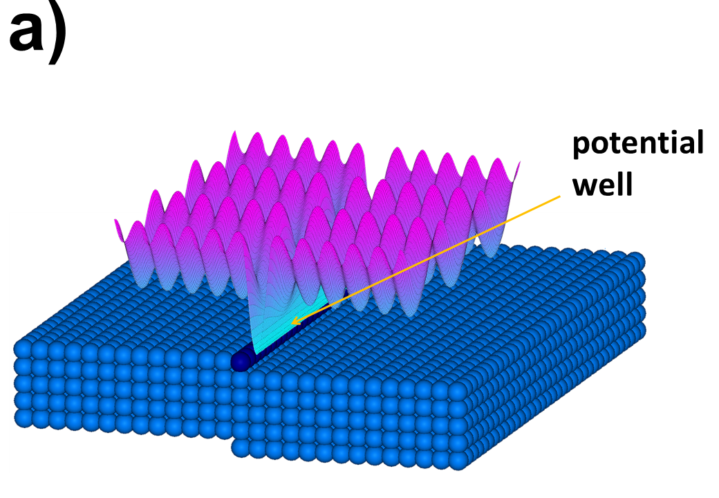
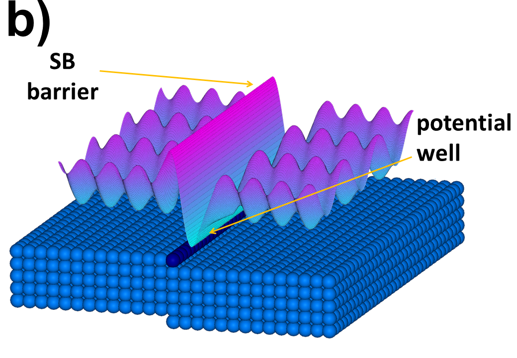
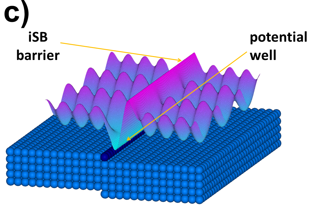
A very important element of the model is energy potential landscape in which all atoms diffuse. Its structure, in particular some important elements of it decide about the formed surface pattern. Three examples of such potentials are shown in Figure 1. We assume that all jumps along the terraces, except for those in the immediate vicinity of the step, are performed with the same probability, which is equal to 1 after the equal choice of jump direction. Sites at the bottom of step have different energy, this is energy well related to the interaction energy with the step [45, 46, 47]. Such situation is illustrated in Fig. 1a. The surface energy landscape in general can have very complex shape, it depends on many different factors, like lattice deformations, surface reconstruction, and all broken bonds at each crystal surface. Due to this there are in this landscape not only potential wells, but also barriers of different types, among them two are the most important ones, having the largest consequences. That are the direct SB barrier at top of the step — illustrated in the Fig. 1b and the inverse iSB barrier at the bottom of steps. They make jumping across the step in the first case or towards step in the second more difficult. We set the probability of such jump and , where is temperature factor and are energies of barriers that have to be overpass by jumping atom. Similarly, probability of jumping out from the potential well is equal to with being the energy difference between of potential well and average energy level.
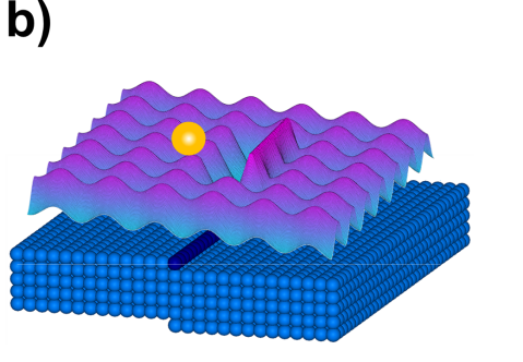
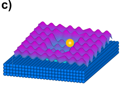
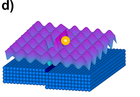
Usually, iSB barrier together with potential well are responsible for the step bunching, while the presence of SB barrier causes meandering process. The aim of our study is to check how additives introduced to the system in binary or ternary crystal can be responsible for step bunching or meandering. To model such situation we prepared system with such surface potential that crystal with it grows smoothly and regularly. It means regular smooth potential with small energy well of order . Such factor means that at temperature of about 700 K the energy is 0.06 eV. Then additives of given concentration replaced atoms at randomly chosen lattice sites. We assume that each of such atoms modifies energy landscape in the way shown in Fig. 2. It means that when the additive is placed at the step, an additional potential well appears below it, and at two neighboring sites. This additional potential well is accompanied by iSB barrier in the first case (Fig. 2a) and SB barrier in the second case (Fig. 2b). We see that both, energy well and energy barrier spread out by three consecutive sites.
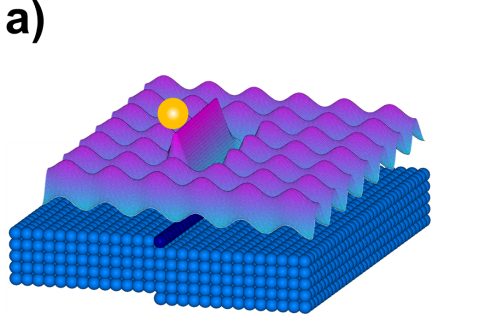
The next case illustrated in Fig. 2c shows the energy well, which causes the molecules to gather inside and increases the probability of nucleation. Then, if this potential appears at the top of the cluster, it becomes the seed for the growth of a nanowire. We will demonstrate such 3D growth in the third example below.
3 Results
3.1 Step bunching and meandering
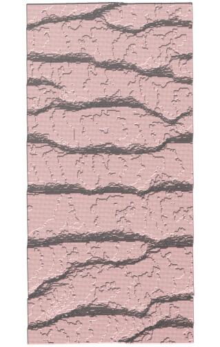
The presence of an inverse barrier at the step is one of the possible and most obvious reasons for the formation of step bunches in the system [19, 22, 23, 26, 38, 40, 44]. It is an energy barrier, occurring at the bottom of the step, one lattice site away from it, as shown in Fig. 2a. Such a barrier stops the flow of particles towards the step from the bottom, which, as can be easily shown by stability analysis, causes the step bunching. Using the VicCA approach, the influence of the inverse step barrier on the step bunching process has been investigated and discussed earlier under different conditions given by the model parameters in 1D [40] and 2D [43] systems. In this work, we show that step bunching is also induced when iSB occurs only at the locations where the additives are attached and in their vicinity, and not along the entire step length.
The simulation typically begins with a regular array with uniformly spaced steps. In our system, we assume low barrier at the bottom of steps, , no barriers of any type present. We started with this low potential value to ensure it would not cause any meandering and that the system would evolve smoothly without any additives, as shown in Fig. 3a. Next we randomly replaced 30% lattice sites with other atoms. Each of these atoms, when positioned on a step, introduces an additional potential well with a depth and an inverse Schwoebel barrier of . Both extend to the next nearest neighboring sites, as shown in Figure 2. Other parameters used in this simulation were , and a system size of . After simulation steps, well-defined bunches were formed, as shown in Fig. 3b. It is clear that the presence of additives, each introducing potential well and an inverse Schwoebel barrier, causes step bunching in an otherwise unbunched system.
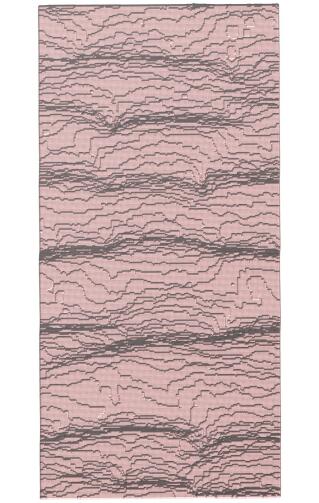
The next case we wanted to study is the opposite situation: the presence SB not iSB in the system. This barrier is known to induce step meandering at the surface [15, 22, 23, 29]. Again we start with the system that has a low potential well at the step, , and replace 20% of the lattice sites with additives. Each additive is associated with a potential well extending over three sites, , and an SB with . Other parameters used were , and the system size was with a simulation time of time steps. After this duration, we observe a well formed meandered structure, which actually develops very quickly.
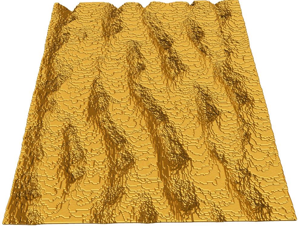
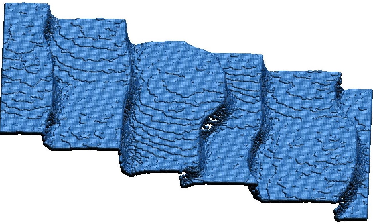
The question now is whether we can smooth the system by eliminating the source of the bunching or meandering process. To test this, after obtaining the bunched structure, we begin supplying the system with only one type of particle. In the Figure 4, the left shows the bunches that formed in the system after simulation steps. The middle panel displays the system after an additional steps, during which only one type of atom was delivered. The final plot on the right illustrates the outcome of the system evolution after growth steps with a single component. It is evident that the crystal continues to grow, and during this process, the step bunches quickly disintegrate, returning to an even distribution once the cause of their formation is removed.
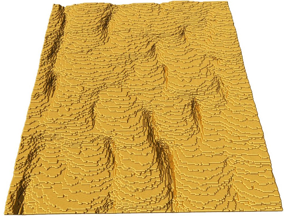
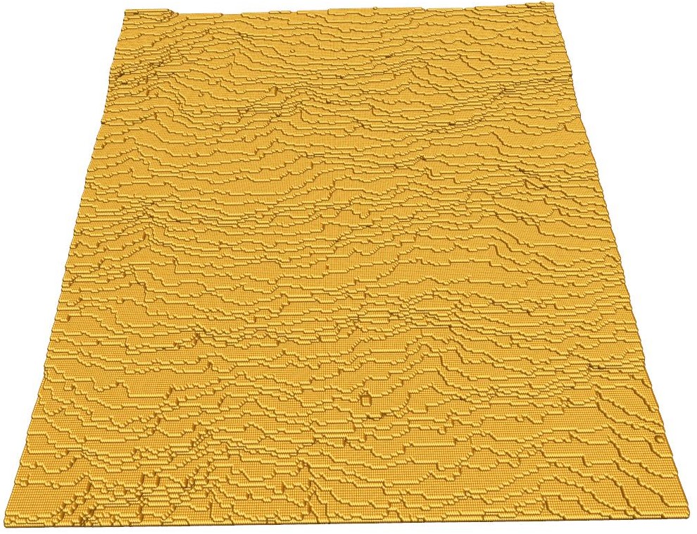
Let’s explore whether the procedure has a similar effect on meandered structures. We applied the method to the system depicted in Fig. 3c, using a slightly smaller system of size while keeping all other parameters identical to those in the previous example. Initially, we generated the meandered structure trough simulation steps (see Fig. 5a). Next, we removed the additives from the incoming flux and allowed a single-component crystal to grow on the meandered structure for additional steps. The resulting configuration is shown in Fig. 5b. The meandered structure appears to smooth out even more rapidly than the bunched structure. The final plot presents the system after evolution steps with single-component flux, where the surface remained notably smooth.
We also examined whether it’s possible to smooth a surface by adding additives instead of removing them. We tested this approach on both bunched and meandered structures by introducing additives with very weak energy potentials into systems with well-formed surface patterns. In both cases, adding these weak potential additives did indeed result in a smoothing effect on the surface shape. However, this method was effective only when the original structures were not too extensive. It appears that large, three-dimensional formations on the surface are significantly more challenging to smooth out.
3.2 3D structures
The examples provided demonstrate that typical surface patterning induced by modifications in surface energy potential due to additives is reversible. Specifically, once a surface patterning mechanism, such as iSB for bunches or SB for meanders, is established, it is relatively straightforward to return to a smooth surface by simply removing the source of instability. However, it remains to be seen whether this observation holds true for all types of surface structures formed during crystal growth. Of particular interest is the behavior of nanowires and similar structures. NWs, for instance, are commonly formed on crystal surfaces under liquid metal droplets, with gold often being used for this purpose. Investigating whether these nanowire structures can be similarly smoothed or removed could provide valuable insights into the generalizability of this reversal process for various surface structures.
The role that the droplet plays in the development of NWs is to accumulate particles under it, so that at higher concentration they can group and build a crystal structure. This accumulation is confined to the area directly under the droplet. Translating this into the context of surface potentials, the droplet effectively creates a potential well in the region it covers, similar to the potential well illustrated in Fig. 2c. This potential well acts as a trap for diffusing atoms, leading to their accumulation and subsequent domain formation. As the NW grows beneath the liquid droplet, the droplet remains positioned atop the NW, causing the process to repeat and the NW to increase in height. This top potential can be accurately modeled using the VicCA approach, as demonstrated in [43, 44].
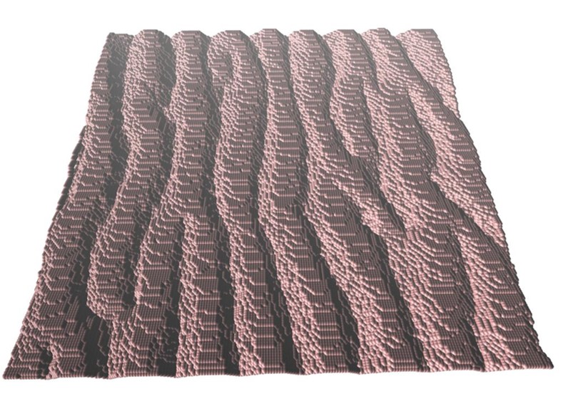
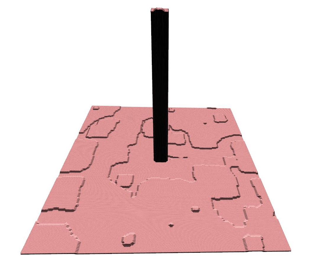
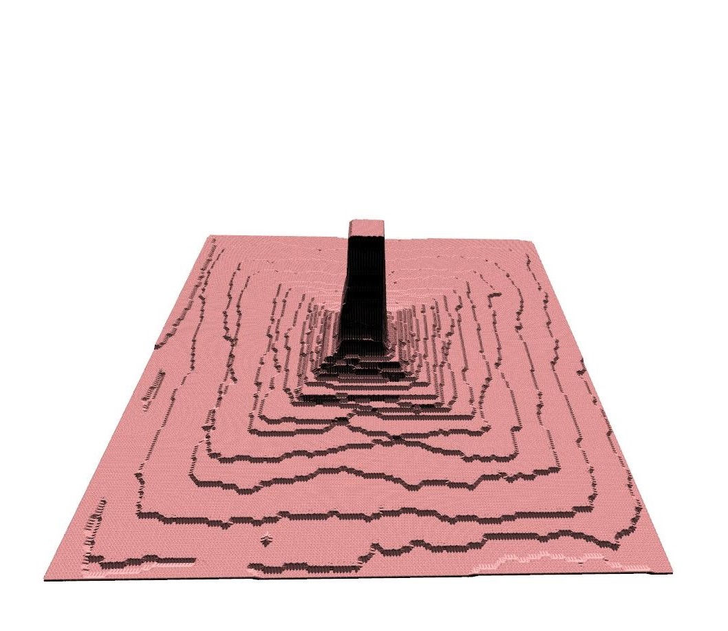
In Figure 6 we present results from simulations where a potential energy well was located at the center of the system. In a lattice area, a potential of was established and maintained for simulation steps. This potential effectively simulates the presence of a gold droplet at the tip of a NW. Under these conditions, the NW forms robustly beneath the droplet and continues to grows as long as the potential conditions are upheld. The surface beneath the NW exhibits square-shaped domains. These domains form with two types of potential wells: one half with at the base of each step for half of the atoms, and the other with at the bottom of the steps for the remaining atoms. The potential energy well helps in concentrating the particles and attaching to the step.A local depression is visible at the foot of the NW. This is because the atoms from the nearest neighborhood tend to the tip of the NW and are adsorbed, powering its growth. The presence of these potential wells aids in concentrating particles and facilitating their attachment to the steps. The simulation assumes a high number of diffusion steps, , corresponding to an effective diffusion coefficient of . The growth process was carried out with a relatively high incoming atom flux, resulting in . After the initial growth step, we removed the central potential well, which physically translates to removing the droplet from the apex of the nanowire. We then continued the growth using the same parameters. Two notable effects occurred: the NW ceased to grow, and an increasing number of atoms began to attach to its base, resulting in the formation of a square pyramid with the remaining fragment of the NW embedded in the center. The outcome after growth steps is illustrated in Figure 6 on the right. During this phase of time evolution, we also set at all sites at the bottom of the steps, which contributed to the rounding of islands. It is evident that further growth, in the absence of the well potential at the top of the NW, begins to smooth the surface; the NW becomes shorter, and a hill forms at its base. This process gradually levels the surface, although significant smoothing is expected only over a very long time. Moreover, various other factors could influence the course of this smoothing process. It is important to note that in real systems, and particularly at considerable heights of NWs, complete surface smoothing is unlikely to be achieved.
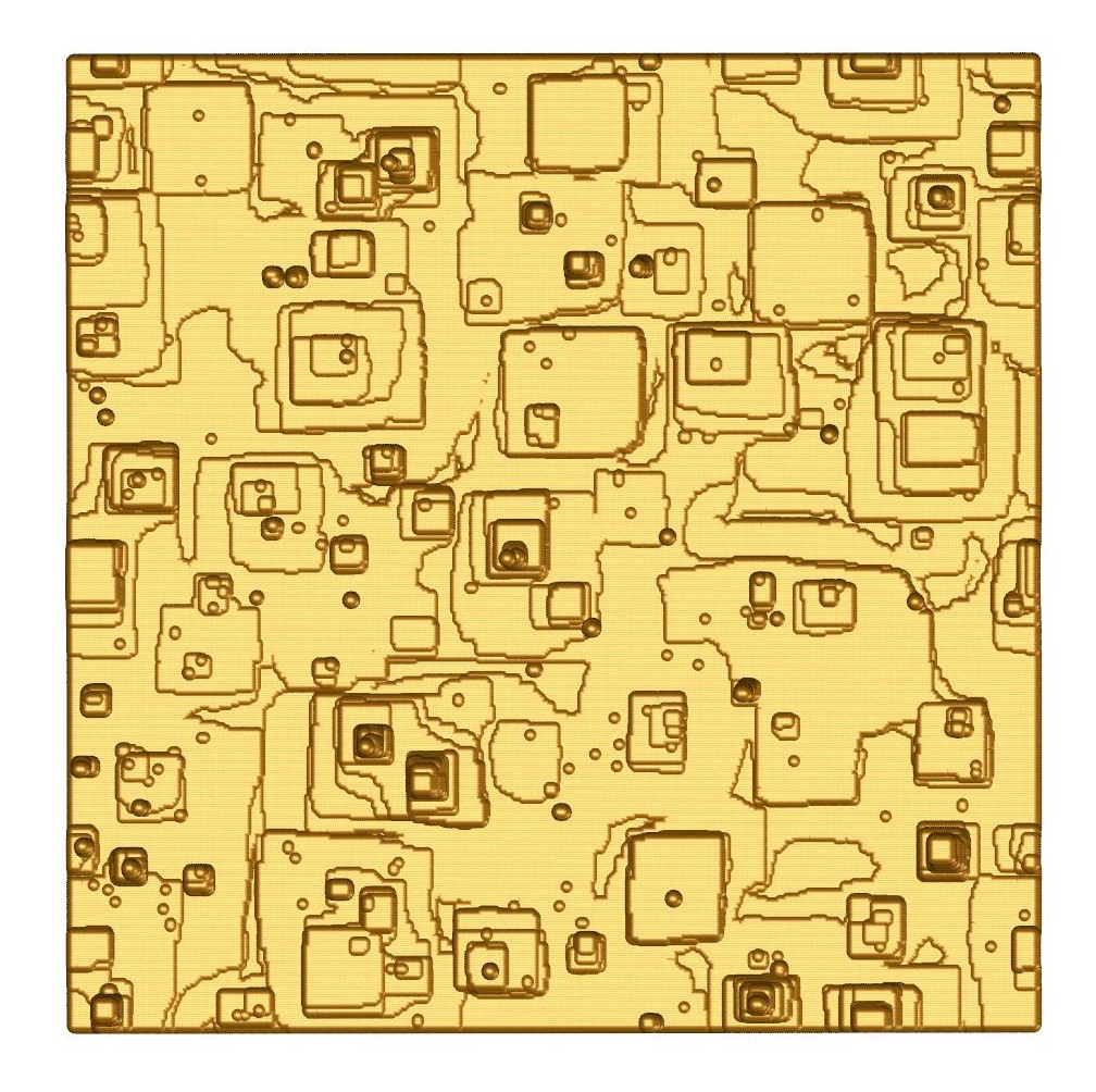
The example provided illustrates the formation of NWs in a homogeneous system, where all atoms adhere to the same rules despite variations in local energy potential. Next, we aim to investigate the behavior of a mixed system containing additives within the crystal to determine whether they can facilitate the formation of NWs. We simulated the system with 40% additives. The majority of the atoms were neutral, without barriers, and a potential well was present at the bottom of the step, specified as . We assumed that the additives create an additional potential well at the edge of the step, as illustrated in Fig. 2d. Each additive, when integrated into the crystal structure at the bottom of the step, introduces a potential well with a depth of , extending along the upper edge of the step for a length covering three adjacent sites. Furthermore, at the position occupied by the additive at the bottom of the step, there exists a small potential well with , and a Svhwoebel barrier of exists between these two sites. Consequently, we constructed the potential structure as follows: the lowest potential is located at the bottom of each step, where a regular atom resides. A slightly higher, yet still low, potential exists at the top of the step, extending to the next three positions and associated with the additive incorporated at the step’s bottom. The smallest potential well corresponds to the site occupied by the additive. It is important to note that in this case, when aiming to grow nanowire structures, we link the additional potential well to the additives at the bottom of the step, rather than at the edges, which is the approach taken when meandering or bunching processes are induced by additional atoms in the crystal structure. To facilitate NW growth, we also modified the cellular automaton rules governing atom attachment to a step. Our intention was to make the attachment process more challenging. Thus, we imposed the condition that two adjacent sites, rather than just one, must be occupied by other atoms for a given atom to attach to the crystal structure at a step. The kink position remains active and does not require any additional conditions. Consequently, we increase the necessity for a higher concentration of adatoms at the step to enable the incorporation of atoms into the crystal structure.
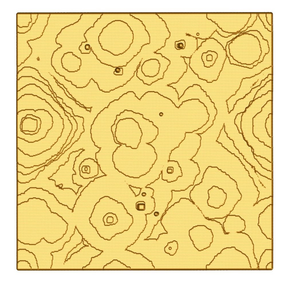
The system was a lattice, starting with very wide terraces of 100 lattice sites each. The simulation results are depicted in Figure 7, showing the top and side views at two different stages of evolution. On the left, we see the structure after simulation steps. On the vicinal surface, two distinct types of structures are visible: flat, square, large islands, and very thin, tall, needle-like nanowires. The simulation was paused at this stage, with the NWs having grown to only about 50 lattice constants in height. Next, we removed the additives from the external stream and continued the simulation for another steps. The right side of the figure shows that the structures have smoothed out over time, with only remnants of the NWs persisting after this extended growth period. Interestingly, the domains transitioned from square to round shapes, a change attributed to the shift from the potential associated with the additives to that of the main atom type. The potential well at the bottom of the steps is much shallower for the basic atom type compared to the additional atoms. As a result, the density of adatoms at the steps increases significantly when the crystal consists solely of the basic atom type. The differences between kink and step positions diminish, leading to the formation of round islands. Consequently, the structures become larger, flatter, and more circular. This simulation highlights how surface potentials, particularly at step edges, critically influence the crystal growth process and the resulting surface patterns. The transition from square to round islands upon changing the external conditions underscores the complex interplay between atomic interactions and external factors such as additives.
4 Conclusions
We conducted an analysis of a process in which semiconductor crystals are modified by substituting some of the atoms in the crystal lattice with additives. This study sheds light on the complex relationship between additives and surface patterns in semiconductor crystals, providing valuable insights into techniques for manipulating and controlling these patterns. To explore this interaction, we used the VicCa model to investigate how the introduction of additives influences the formation of new surface structures. These patterns arise due to the altered interactions and dynamics within the crystal lattice induced by the additives. In the model, we can precisely control the effects of additives on the crystal structure by altering the potential energy landscape. By adjusting this potential, we can induce various surface phenomena, such as meandering, bunching, or the formation of more intricate structures like nanowires. Once these new surface structures are formed, they can be smoothed by applying successive layers of a homogeneous composition over the modified crystal. Over time, this process helps to reduce the irregularities introduced by the additives.
Additives can also be employed to smooth pre-existing surface patterns in a homogeneous crystal. However, the effectiveness of this approach depends on the nature of the surface pattern. For simpler patterns, this method can be quite effective, but for more complex, spatially extended patterns like nanowires, applying homogeneous layers is less successful. In such cases, the surface may not be fully smoothed; instead, it may adopt a different shape after treatment. Our study delves into the mechanisms underlying this behavior, exploring how both the presence of additives and the application of homogeneous layers influence the final surface structure of the crystal. This research enhances our understanding of how to control and optimize surface morphologies in semiconductor materials.
Acknowledgments
The authors thank The Polish National Center for Research and Development (grant no. EIG CONCERT-JAPAN/9/56/AtLv-AlGaN/2023) for financial support.
References
- [1] Y. Oreg, G. Refael, F. von Oppen, Helical Liquids and Majorana Bound States in Quantum Wires, Phys. Rev. Lett. 105 (2010), 177002. https://doi.org/10.1103/PhysRevLett.105.177002.
- [2] R. M. Lutchyn, J. D. Sau, S. Das Sarma, Majorana Fermions and a Topological Phase Transition in Semiconductor-Superconductor Heterostructures, Phys. Rev. Lett. 105 (2010), 077001. https://doi.org/10.1103/PhysRevLett.105.077001.
- [3] V. Mourik, K. Zuo, S. M. Frolov, S. R. Plissard, E. P. A. M. Bakkers, L. P. Kouwenhoven, Signatures of Majorana Fermions in Hybrid Superconductor-Semiconductor Nanowire Devices, Science 336 (2012),1003–1007. https://doi.org/10.1126/science.1222360.
- [4] P. Grünberg, R. Schreiber, Y. Pang, M. B. Brodsky, H. Sowers, Layered Magnetic Structures: Evidence for Antiferromagnetic Coupling of Fe Layers across Cr Interlayers, Phys. Rev. Lett. 57 (1986), 2442. https://doi.org/10.1103/PhysRevLett.57.2442.
- [5] M. N. Baibich, J. M. Broto, A. Fert, V. D. F. Nguyen, F. Petroff, P. Etienne, G. Creuzet, A. Friederich, J. Chazelas, Giant Magnetoresistance of (001)Fe/(001)Cr Magnetic Superlattices, Phys. Rev. Lett. 61 (1988), 2472. https://doi.org/10.1103/PhysRevLett.61.2472.
- [6] C. Fermon, M. Pannetier-Lecoeur, Noise in GMR and TMR Sensors, in: C. Reig, S. Cardoso, S.C. Mukhopadhyay (Eds.), Giant Magnetoresistance (GMR) Sensors. Smart Sensors, Measurement and Instrumentation; Springer: Berlin/Heidelberg, Germany, 2013; Volume 6, pp. 47–70.
- [7] N. Zheludev, The life and times of the LED — A 100-year history, Nat. Photonics 1 (2007), 189–192. https://doi.org/10.1038/nphoton.2007.34.
- [8] J. J. Yang, M. D. Pickett, X. Li, D. A. A. Ohlberg, D. R. Stewart, R. S. Williams, Memristive switching mechanism for metal/oxide/metal nanodevices, Nat. Nanotechnol. 3 (2008), 429–433. https://doi.org/10.1038/nnano.2008.160.
- [9] J. J. Yang, D. B. Strukov, D. R. Stewart, Memristive Devices for Computing, Nat. Nanotechnol. 8 (2013), 13–24. https://doi.org/10.1038/nnano.2012.240.
- [10] R. Verre, K. Fleisher, J. F. McGlip, D. Fox, G. Behan, H. Zhang, I. V. Shvets, Controlled in situ growth of tunable plasmonic self-assembled nonoparticle array, Nanotechnology 23 (2012), 035606. https://dx.doi.org/10.1088/0957-4484/23/3/035606.
- [11] G. Yao, M. Gao, Y. Ji, W. Liang, L. Gao, S. Zheng, Y. Wang, B. Pang, Y. B. Chen, H. Zeng, H. Li, Z. Wang, J. Liu, C. Chen, Y. Lin, Surface step terrace tuned microstructures and dielectric properties of highly epitaxial CaCu3Ti4O12 thin films on vicinal LaAlO3 substrates, Sci. Rep. (2016), 6, 34683. https://doi.org/10.1038/srep34683.
- [12] V. Usov, C. O. Coileain, I. V. Shvets Experimental quantitive study into the efects of electromigration field moderation on step bunching instability, Phys. Rev. B (2011), 83, 155321. https://doi.org/10.1103/PhysRevB.83.155321.
- [13] X. Q. Shen, H. Okamura, Surface step morphologies of GaN films grown on vicinal sapphire (0001) substrate by rf-MBE, J. Cryst. Growth (2007), 300, 75-78. https://doi.org/10.1016/j.jcrysgro.2006.10.206.
- [14] H. Omi, Y. Homma, V. Tonchev, A. Pimpinelli, New Types of Unstable Step-Flow Growth on Si(111)-(7x7) during Molecular Beam Epitaxy: Scaling and Univeraslity, Phys. Rev. Lett. (2005), 95, 216101. https://doi.org/10.1103/PhysRevLett.95.216101.
- [15] H. Turski, F. Krzyżewski, A. Feduniewicz-Żmuda, P. Wolny, M. Siekacz, G. Muziol, C. Cheze, K. Nowakowski-Szukudlarek, H. G. Xing, D. Jena, M. Załuska-Kotur, C. Skierbiszewski, Unusual step meandering due to Ehrlich-Schwoebel barrier in GaN epitaxy on the N-polar surface, Appl. Surf. Sci. (2019), 484, 771–780. https://doi.org/10.1016/j.apsusc.2019.04.082.
- [16] M. Sawicka, H. Turski, K. Sobczak, A. Feduniewicz-Żmuda, N. Fiuczek, O. Gołyga, M. Siekacz, G. Muziol, G. Nowak, J. Smalc-Koziorowska, C. Skierbiszewski, Nanostars in Highly Si-Doped GaN, Cryst. Growth Des. (2023), 23, 5093–5101. https://pubs.acs.org/doi/10.1021/acs.cgd.3c00317
- [17] D. J. Liu, J. D. Weeks, Quantitive theory of current-induced step bunching on Si(111), Phys. Rev. B (1998), 57, 14891-14900. https://doi.org/10.1103/PhysRevB.57.14891.
- [18] A. Pimpinelli, V. Tonchev, A. Videcoq, M. Vladimirova, Scaling and Universality of Self-Organized Patterns on Unstable Vicinal Surfaces, Phys. Rev. Lett. (2002), 88, 206103. https://doi.org/10.1103/PhysRevLett.88.206103.
- [19] J. Krug, V. Tonchev, S. Stoyanov, A. Pimpinelli, Scaling properties of step bunches induced by sublimation and related mechanisms, Phys. Rev. B (2005), 71, 045412. https://doi.org/10.1103/PhysRevB.71.045412.
- [20] V. Tonchev, B. Ranguelov, H. Omi, A. Pimpinelli, Scaling and universality in models of step bunching: the ”C+-C-” model, Eur. Phys. J. B (2010), 73, 539-546. https://doi.org/10.1140/epjb/e2010-00036-3.
- [21] S. Stoyanov, Current induced step bunching at vicinal surfaces during crystal evolution, Surface Science (1997), 370, 345-354. https://doi.org/10.1016/S0039-6028(96)00966-1.
- [22] F. Krzyżewski, M. Załuska Kotur, Stability diagrams for surface patterns of GaN() as a function of Schwoebel barrier height, J. Crys. Growth (2017), 457, 80-84. https://doi.org/10.1016/j.jcrysgro.2016.04.043.
- [23] C. Misbah, O. Pierre-Louis, Y. Saito, Crystal surfaces in and out of equilibrium: A modern view, Rev. Mod. Phys. (2010), 82, 981-1040. https://doi.org/10.1103/RevModPhys.82.981.
- [24] S. Krukowski, K. Sakowski, P. Strak, P. Kempisty, J. Piechota, I. Grzegory, Macrosteps dynamics and the growth of crystals and epitaxial layers, Progress in Crystal Growth and Characterization of Materials (2022), 68, 100581. https://doi.org/10.1016/j.pcrysgrow.2022.100581.
- [25] R. L. Schwoebel, Step motion on crystal surfaces. II, J. Appl. Phys. (1969), 40, 614-618. https://doi.org/10.1063/1.1657442.
- [26] M. Sato, M. Uwaha, Growth law of step bunches induced by the Ehrlich-Schwoebel efect, Surface Sci. (2001), 493, 494-498. https://doi.org/10.1016/S0039-6028(01)01258-4.
- [27] M. H. Xie, S. Y. Leung, S. Y. Tong, What causes step bunching - negative Ehrlich-Schwoebel barrier versus positive incorporation barrier, Surface Sci. (2002), 515, L459-L463. https://doi.org/10.1016/S0039-6028(02)01976-3
- [28] R. L. Schwoebel, E. J. Shipsey, Step motion on crystal surfaces, J. Appl. Phys. (1966), 37, 3682-3686. https://doi.org/10.1063/1.1707904.
- [29] F. Krzyżewski, M. A. Załuska-Kotur, Coexistence of bunching and meandering instability in simulated growth of 4H-SiC(0001) surface, J. Appl. Phys. (2014), 115, 213517. https://doi.org/10.1063/1.4881816.
- [30] J.-H. Kang, F. Krizek, M. Za luska-Kotur, P. Krogstrup, P. Kacman, H. Beidenkopf, H. Shtrikman, Au-Assisted Substrate-Faceting for Inclined Nanowire Growth, Nano Letters (2018), 18, 4115-4122. https://doi.org/10.1021/acs.nanolett.8b00853
- [31] S. K. Arora, B. J. O’Dowd, B. Ballesteros, P. Gambardella, I. V. Shvets, Magnetic properties of planar nanowire arrays of Co fabricated on oxidized step-bunched silicon templates, Nanotechnology (2012), 23, 235702. https://doi.org/10.1088/0957-4484/23/23/235702
- [32] A. Krasteva, H. Popova, F. Krzyżewski, M. Załuska-Kotur, V. Tonchev, Unstable vicinal crystal growth from cellular automata, AIP Conf. Proc. (2016), 1722, 220014. https://doi.org/10.1063/1.4944246.
- [33] K. Sudoh, H. Iwasaki, Step dynamics in faceting on vicinal Si(113) surfaces, J. Phys.: Condens. Matter (2003), 15, S3241. https://doi.org/10.1088/0953-8984/15/47/004
- [34] N. Néel, T. Maroutian, L. Douillard and H.-J. Ernst, Spontaneous structural pattern formation at the nanometre scale in kinetically restricted homoepitaxy on vicinal surfaces, J. Phys.: Condens. Matter (2003), 15, S3227. https://doi.org/10.1088/0953-8984/15/47/003
- [35] T. S. Rahman, A. Kara, S. Durukanoglu, Structural relaxations, vibrational dynamics and thermodynamics of vicinal surfaces, J. Phys.: Condens. Matter (2003), 15, S3197. https://doi.org/10.1088/0953-8984/15/47/002.
- [36] H. Minoda, Direct current heating effects on Si(111) vicinal surfaces, J. Phys.: Condens. Matter (2003), 15, S3255. https://doi.org/10.1088/0953-8984/15/47/005.
- [37] S. Rousset, V. Repain, G. Baudot, Y. Garreau, J. Lecoeur, Self-ordering of Au(111) vicinal surfaces and application to nanostructure organized growth, J. Phys.: Condens. Matter (2003), 15, S3363. https://doi.org/10.1088/0953-8984/15/47/009.
- [38] F. Krzyżewski, M. A. Załuska-Kotur, A. Krasteva, H. Popova, V. Tonchev, Step bunching and macrostep formation in 1D atomistic scale model of unstable vicinal crystal growth, J. Cryst. Growth (2017), 474, 135-139. https://doi.org/10.1016/j.jcrysgro.2016.11.121.
- [39] O. Toktarbaiuly, V. O. Usov, C. Coileáin, K. Siewierska, S. Krasnikov, E. Norton, S. I. Bozhko, V. N. Semenov, A. N. Chaika, B. E. Murphy, O. Lübben, F. Krzyżewski, M. A. Załuska-Kotur, A. Krasteva, H. Popova, V. Tonchev, I. V. Shvets, Step bunching with both directions of the current: Vicinal W(110) surfaces versus atomistic-scale model, Phys. Rev. B (2018), 97, 035436. https://doi.org/10.1103/PhysRevB.97.035436.
- [40] F. Krzyżewski, M. A. Załuska-Kotur, A. Krasteva, H. Popova, V. Tonchev, Scaling and Dynamic Stability of Model Vicinal Surfaces, Cryst. Growth Des. (2019), 19, 821-831. https://doi.org/10.1021/acs.cgd.8b01379.
- [41] H. Popova, F. Krzyżewski, M. A. Załuska-Kotur, V. Tonchev, Quantifying the Effect of Step–Step Exclusion on Dynamically Unstable Vicinal Surfaces: Step Bunching without Macrostep Formation, Cryst. Growth Des. (2020), 20, 7246-7259. https://doi.org/10.1021/acs.cgd.0c00927
- [42] H. Popova, Analyzing the Pattern Formation on Vicinal Surfaces in Diffusion-Limited and Kinetics-Limited Growth Regimes: The Effect of Step–Step Exclusion, Cryst. Growth Des. (2023), 23, 8875–8888. https://doi.org/10.1021/acs.cgd.3c00952.
- [43] M. Załuska-Kotur, H. Popova, V. Tonchev, Step Bunches, Nanowires and Other Vicinal ”Creatures” - Ehrlich–Schwoebel Effect by Cellular Automata, Crystals (2021), 11, 1135. https://doi.org/10.3390/cryst11091135.
- [44] M. A. Chabowska, M. Załuska-Kotur, Diffusion-Dependent Pattern Formation on Crystal Surfaces, ACS Omega, (2023), 8, 45779-45786. https://doi.org/10.1021/acsomega.3c06377.
- [45] T. Ohka, T. Akiyama, A. Muizz Pradipto, K. Nakamura, T. Ito, Effect of Step Edges on Adsorption Behavior for GaN(0001) Surfaces during Metalorganic Vapor Phase Epitaxy: An Ab Initio Study, Cryst. Growth Des. (2020), 20, 4358-4365. https://doi.org/10.1021/acs.cgd.0c00117
- [46] T. Akiyama, T. Ohka, K. Nagai, T. Ito, Effect of step edges on the adsorption behavior on vicinal AlN(0001) surface during metal-organic vapor phase epitaxy: An ab initio study, J. Cryst. Growth (2021), 571, 126244. https://doi.org/10.1016/j.jcrysgro.2021.126244.
- [47] T. Akiyama, T. Kawamura, Ab initio study for adsorption behavior on AlN(0001) surface with steps and kinks during metal-organic vapor-phase epitaxy, Jpn. J. Appl. Phys. (2024), 63, 02SP71. https://doi.org/10.35848/1347-4065/ad1896