Digital stabilization of an IQ modulator in the carrier suppressed single side-band (CS-SSB) mode for atom interferometry
††journal: opticajournal††articletype: Research ArticleWe present an all-digital method for stabilising the phase biases in an electro-optic I/Q modulator for carrier-suppressed single-sideband modulation. Building on the method presented in S. Wald et al., Appl. Opt. 62, 1-7 (2023), we use the Red Pitaya STEMlab 125-14 platform to digitally generate and demodulate an auxiliary radio-frequency tone whose beat with the optical carrier probes the I/Q modulator’s phase imbalances. We implement a multiple-input, multiple-output integral feedback controller which accounts for unavoidable cross-couplings in the phase biases to lock the error signals at exactly zero where optical power fluctuations have no impact on phase stability. We demonstrate suppression of the optical carrier relative to the desired sideband at over a period of hours and over temperature variations of .
1 Introduction
Many quantum technologies, such as sensors [1, 2, 3, 4, 5, 6, 7, 8, 9], memories [10, 11, 12, 13, 14], and computers [15, 16, 17], rely on the coherent manipulation of quantum states of neutral atoms using two or more lasers at different frequencies which have a stable phase relationship while simultaneously being tunable [18], spectrally pure [19], and high power [20, 21, 18]. In the case of systems using alkali metal atoms, such as rubidium and cesium, these frequencies are often separated by several GHz corresponding to the ground-state hyperfine splitting [1, 13, 15], which complicates coherent frequency synthesis. Quantum sensors and memories may also be deployed in the field [22, 23, 24, 6] which further requires the laser system to be robust to environmental changes and, particularly for quantum sensors, to have low size, weight, and power (SWaP) [20, 8].
One method for generating phase-coherent frequencies at GHz separations is to modulate the phase of the laser using an electro-optic modulator (EOM) [25, 23, 26]. Sinusoidal modulation of the phase yields sidebands symmetrically located on either side of the carrier frequency at multiples of the modulation frequency. By interferometrically combining the output laser fields from several EOMs, usually in a single fibre-coupled waveguide structure, unwanted spectral components can be suppressed. In particular, the so-called dual-parallel Mach-Zehnder interferometer (MZI) structure creates an I/Q modulator that allows independent control of the amplitude and phase of the light [27]. Careful tuning of the phase biases of the internal MZIs allows the modulator to operate in the carrier-suppressed single sideband (CS-SSB) mode where nearly all of the optical power is in one of the sidebands. As these phase biases are prone to drift, especially due to temperature but also due to photorefractive damage [28, 29], they need to be actively stabilised at the correct operating point. The most common scheme involves modulating the phase biases at the level [30, 18] which is transferred to the optical signal and then detected and demodulated to form an error signal. The disadvantage of this method is that the output laser power now varies at the modulation frequency, which can lead to pulse area errors in the manipulation of quantum states.
An alternative stabilisation method was proposed by Wald et al.[31] in which a weak auxiliary radio-frequency (RF) tone is added to the main microwave tone. Demodulation of the measured optical power at the RF tone and its second harmonic yields signals that measure the amplitude of the carrier and unwanted sideband. When operating in CS-SSB mode only one sideband from each frequency is present, and the beatnote between these frequencies is on the order of GHz, eliminating the effect of amplitude modulation on the manipulation of quantum states. Stabilisation of the phase biases was achieved using analog electronics and three independent feedback loops; however, cross-coupling between the interferometer phase biases meant that the error signals had to be stabilised away from zero. This leads to the possibility that the spectral purity of the output mode can be compromised by changes in the input laser power or in the environment.
Building on the work presented in [31], we present an all-digital system for stabilising the phase biases in an I/Q modulator for CS-SSB operation. We use the fast analog input and output capabilities of the Red Pitaya STEMlab 125-14 platform, combined with high-speed programmable logic, to implement a digital multiple-input, multiple-output (MIMO) feedback loop that compensates for cross-coupling of the phase biases and allows locking of the measured signals at exactly zero. Direct access to the system’s transfer function allows us to automatically and efficiently tune the feedback loop. We demonstrate stable operation of our system over long periods of time () and large temperature variations ().
2 Carrier-suppressed single sideband generation
We consider an I/Q modulator in the dual parallel Mach-Zehnder interferometer (MZI) configuration as shown in Fig. 1 with a single modulation frequency . A field of amplitude with carrier frequency is applied to the I/Q modulator which gets split into four initial paths, each of which goes through a phase modulator. These phase modulators are arranged in a pair of MZIs, with one pair (1-2) being driven by signals and the other (3-4) being driven by . In addition to the modulation, we also apply phases , , , and to each of the phase modulators. The output fields and of the sub-MZIs are subject to additional phase shifts and and are then passed through the outer MZI to get the final output field .
Consider a phase modulation of the form with an amplitude such that
| (1) |
The fields for the sub-MZIs 1-2 are given by
| (2) | ||||
| (3) |
and hence the field at the output of sub-MZI at is
| (4) |
where we have defined the average phase and differential phase . When the carrier at is suppressed, and we are left with only sideband amplitudes at . For good suppression, which is when the carrier amplitude is much less than the sideband amplitude, the condition must be satisfied. Similarly, the field at can be written as
| (5) |
where and . The output field is then
| (6) |
with and . The carrier is suppressed when , and by setting the positive or negative sideband can be selected to give CS-SSB operation.

The relative amplitudes of the various sidebands can be determined by measuring the total power using a photodetector with a bandwidth and is
| (7) |
where the first line is the DC power in the different frequency components, the second line is the beatnote between the carrier and sidebands, and the third line is the beatnote between the sidebands. Near the CS-SSB operating point, where and , we have
| (8) |
which implies that the amplitudes of the photodetector signals at and are linear in the phase biases and thus can be used as error signals for locking the phase biases at the correct operating points [31]. Note that according to Eq. (7) if , which corresponds to carrier-only operation, our error signals will also be near zero and linear in phase deviations about that point, so for this locking scheme to work it needs to start close to the desired CS-SSB set-point by using auxiliary information such as known voltage biases for the I/Q modulator or an optical spectrum analyzer.
3 Experimental setup
Our optical and electronic setup is shown in Fig. 2. A narrow-linewidth fiber laser (NKT Photonics Koheras Basik) is used as a seed laser that generates of laser light at . The laser beam is then passed through a fiber beam-splitter where is used as an input to the I/Q modulator (iXblue MXIQ-LN-30), while the remainder is used as a source for a fibre-coupled acousto-optic modulator (AOM, G&H 80MHz Fiber-Q). A microwave synthesizer generates a high frequency signal at which is first amplified and then passed through a hybrid power splitter (Mini Circuits ZX 100-2-34-S+) to get two signals with a phase difference of at a power of . We combine the microwave signals with two low-frequency () signals that are out of phase generated by the fast analog outputs of a Red Pitaya STEMlab 125-14 board (power of ) using a pair of diplexers (Marki DPXN-OR5) which then also drive the two RF ports of the I/Q modulator. Three pulse-width modulation (PWM) outputs from the RP with bit resolution clocked at are amplified and filtered with a corner frequency of to drive the three phase biases on the I/Q modulator.
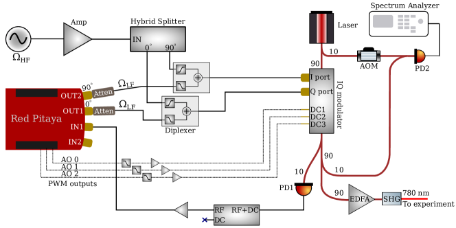
After the I/Q modulator, we split the laser using two fiber beam-splitters such that of the light impinges on the feedback photodetector (PD1, Thorlabs DET01CFC), is combined with the light that passes through the AOM and is measured with a fast photodetector (PD2, Thorlabs DET08C), and passes through an erbium-doped fiber amplifier (Civil Laser EDFA-C-BA-23-PM-M) which is then frequency doubled using a waveguide second harmonic generator (SHG, Covesion WGCO-H-1560-40) crystal to produce light at for our rubidium atom interferometry experiments [18, 20]. All fibre components use polarization maintaining fibre.
The signal from PD1 passes through an RF bias-tee to remove the DC component and is then amplified by before being recorded using one of the fast analog inputs on the RP, and this serves as the source for feedback error signals. With the AOM shifting the frequency of the carrier by , the spectrum measured at PD2 can unambiguously measure the power in each of the frequencies produced by the I/Q modulator and allows for out-of-loop measurements of the system’s performance.
4 Digital stabilisation of phase biases
We use the field-programmable gate array (FPGA) on-board the RP for digital stabilization of the phase biases of the I/Q modulator. Digital feedback loops offer several advantages over analog feedback loops: set-points have no noise or drift, the system is both easily modified and highly portable to other experiments, and complex control laws are readily implemented. The major disadvantages of digital loops are that they can suffer from digitisation noise on inputs and outputs, and they tend to have lower loop bandwidths due to the latency of digital operations. However, for stabilising the phase biases neither of these potential drawbacks cause problems. We amplify the input signal and use a sufficiently large PWM bit depth so that digitisation noise is not a limiting factor. Changes in the phase biases are typically thermally-driven, with timescales on the order of , which are long enough that digital latency (on the order of ) is a negligible contribution to the loop delay.
Our implementation uses three direct digital synthesis (DDS) modules, one of which drives the two analog outputs at and . The other two DDSs generate signals , , and with demodulation phases and which are multiplied with the input signal and then filtered using third-order cascaded integrator-comb (CIC) filters to produce a vector of measurements . The CIC filters also reduce the sampling rate so that the measurements can be more easily processed and stored for later analysis: we use a rate reduction of for a sample rate of which is much faster than the timescales at which the phase biases change. From Eqs. (7) and (8), the measurements are approximately
| (9) |
with overall measurement scaling . Ideally, the phase biases can be adjusted independently, so by correctly choosing the demodulation phases (in this instance ) we maximize the measurement amplitudes and minimize cross-coupling between measurements. In practice, the DC voltages used to change the phase biases couple significantly to the other biases, and it is impossible to entirely eliminate cross-coupling.
To appropriately account for cross-coupling between and we use a discretized multiple-input multiple-output (MIMO) integral control law, so that for static set-points and feedback matrix . We implement the control law in programmable logic using a time-shared multiplier to reduce system resources ( multiplier instead of ), as the additional latency () is negligible compared to other timescales. We model the response of the measurements to changes in near the CS-SSB operating point as a first-order low-pass filter with steady-state transfer function and diagonal decay rate matrix
| (10) |
where the decay rates are dominated by the PWM low-pass filter rather than the inherent response of the I/Q modulator’s phase bias ports or by the measurement filter response. The closed-loop behaviour is then a second-order dynamical system
| (11) |
By measuring and , we can choose a feedback matrix such that is diagonal, which minimizes cross-coupling of measurement noise and environmental perturbations, and has eigenvalues close to those required for critical damping.
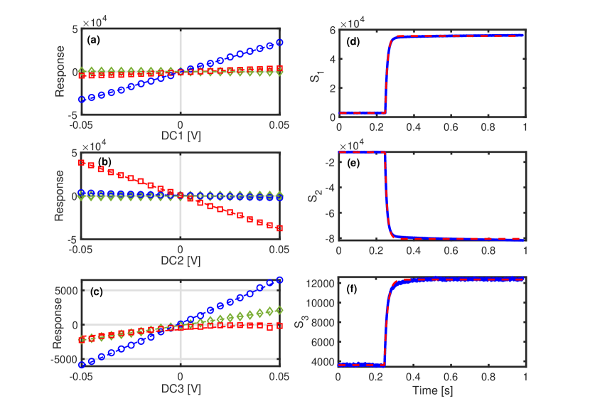
We automatically tune our control system in several steps. First, we determine the demodulation phase by fixing DC1 and DC2 and varying DC3 over its full range for demodulation phases : the optimum value of is where the amplitude of as a function of DC3 is maximal as seen in Eq. (7). At this demodulation phase, we then vary DC3 and locate the values at which which correspond to . Picking the desired sideband, we then vary DC2 with DC1 and DC3 fixed for several demodulation phases and measure where the response of is a maximum as a function of DC2: this is the optimum phase . We individually measure versus DC1 and versus DC2 and find where ; here, one needs additional information because = 0 both when the carrier is suppressed and when both sidebands are suppressed. After picking the correct operating point, we measure by making small changes to each of the DC voltages and measuring the linear response of in the steady state as shown in Figs. 3a-c. We measure by making a step change in and measuring the relaxation of to its steady state as shown in Figs. 3d-f. We then choose a diagonal target feedback matrix such that ; the elements of are the squares of the natural frequencies of the decoupled harmonic oscillators in Eq. (11). One then aims for to achieve critical damping.
5 Characterization
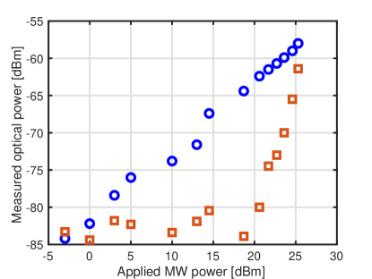
In order to investigate the stability of the I/Q bias lock and to characterise the quality of CS-SSB operation, we use the out-of-loop measurement scheme shown in Fig. 2 which overlaps the output of the I/Q modulator with a frequency-shifted copy of the carrier and measures the resulting signal using a fast photodiode and spectrum analyzer. We first measure the suppression of the carrier relative to the positive sideband for different applied microwave powers as shown in Fig. 4. We engage the bias lock with set-points of zero for all signals at the lowest microwave power, and then we gradually increase the microwave power with the lock engaged while measuring the optical power in the carrier and positive sideband. We find that the sideband power increases linearly with microwave power over the entire investigated range, implying that we are operating in a phase modulation regime where we can neglect higher modulation sidebands. However, the carrier power is constant only for low microwave powers and increases as otherwise. Further investigation has shown that the combined presence of signals at and leads to the generation of additional amplitude on the optical signal which interferes with the signal used for bias stabilisation. This leads to the condition no longer being the CS-SSB operating point. Choosing allows us to reduce the measured carrier power, but this raises the possibility that the lock stability now depends on the input optical power, insertion loss, and modulation depth which can change with environmental conditions or with time [28, 29]. Instead, we reduce the microwave power to so that we can continue operating with at the cost of a factor of two in sideband power, which in our case can be compensated with an optical pre-amplifier.
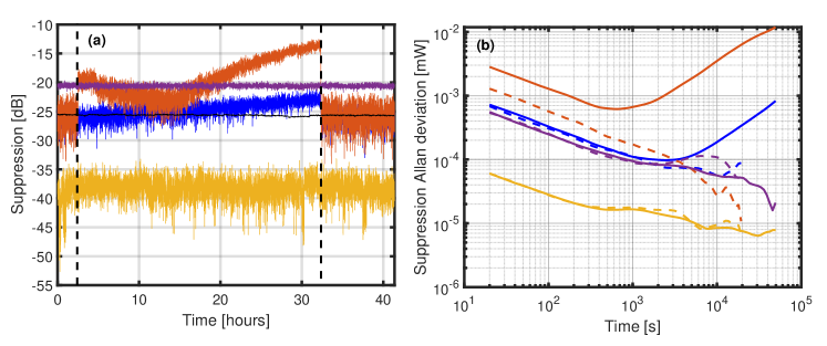
Figure 5a presents a time-series measurement illustrating the difference in stability between the locked and unlocked states. When the biases are unlocked there is significant drift in the carrier suppression over the course of about day with a much smaller change in the suppression of the sideband. The power in the sidebands remains approximately constant. When the biases are locked, the carrier and sideband are stabilised to powers that are on average below the positive sideband. This suppression is limited by noise on the measurements , corresponding to noise on the signal within the CIC filter bandwidth of . This noise is likely from the photodetector and amplifiers used to measure the optical power, as the expected noise contributed by the RP ADC is a factor of lower than what is measured. An Allan deviation analysis of the locked and unlocked data (in between the vertical black dashed lines) is shown in Fig. 5b, which shows that the I/Q modulator tends to drift away from CS-SSB operation on the time-scale of about when feedback is disengaged. When the biases are locked, suppression remains stable for times .
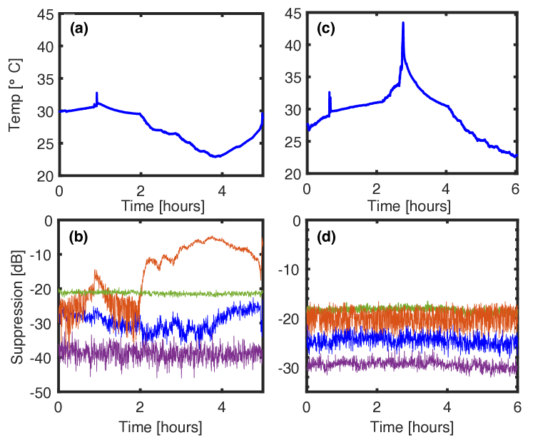
Figure 6 demonstrates time-series measurements of the suppressed carrier and unwanted sidebands with large temperature swings that we induce with a heat gun and by changing the temperature of the laboratory. We observe that the locked system remains stable against large temperature variations over many hours, whereas the unlocked system displays large excursions from the CS-SSB operating mode. Stability against temperature variations is especially critical for field-deployable quantum technologies such as quantum sensors or repeaters which may be subjected to large changes in their operating environment.
Stable, high suppression of unwanted frequency components is especially critical for atom interferometry, as the additional spectral components can cause large systematic phase shifts through longitudinal variation in the phase of the two-photon Raman Rabi frequency [19, 18]. In our experiment, the I/Q modulator path drives one of the lasers in the Raman transition, while the other laser is generated by amplifying and doubling the seed laser but with no frequency modifications to produce a laser at the same frequency as the carrier from the I/Q modulator. Adapting the model presented in Ref. [18], and assuming that the ratio of optical powers in the carrier frequency and positive sideband frequency are chosen to minimise the differential AC Stark shift [32], we calculate the maximum systematic error that would be seen with our laser system in Fig. 7.
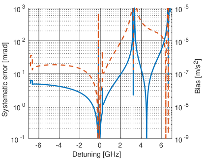
We find that the unwanted sidebands contribute at most ( for a interferometer) to the systematic error for Raman laser detunings from to , while the unlocked system can reach systematic errors of up to () in that same region when ignoring detunings close to zero.
6 Conclusions
In this article, we presented a laser system based on digital stabilization of an I/Q modulator in the CS-SSB mode for state preparation and manipulation in quantum technologies and especially atom interferometers for inertial sensing. The phase biases of the I/Q modulator were measured and stabilized by an all-digital feedback circuit utilizing the programmable logic and fast analog input/output capabilities of the Red Pitaya STEMlab 125-14 platform. Careful application of microwave power and the use of a MIMO integral feedback controller allowed us to stabilise the measured signals at set-points of zero, reducing sensitivity of the lock to changes in input power, insertion loss, or modulation depth. We demonstrated carrier and negative sideband suppression of relative to the desired positive sideband with the auxiliary tone at being below the sideband. CS-SSB operation was demonstrated with the lock engaged for and under severe temperature changes. We have already deployed our system for two atom interferometry experiments and have observed that the lock is maintained for weeks at a time even though the I/Q modulator is located next to the heating and cooling system for the laboratory. Calculations predict that the systematic error resulting from the residual sidebands will be on the order of , which corresponds to a part-per-billion accuracy in the measurement of terrestrial gravity using a modest interferometer time of .
The fast analog and digital control system presents opportunities for future improvements for reducing statistical and systematic errors. Suppression of unwanted sidebands is likely limited by detection noise, but the signal-to-noise ratio of the measurement can be improved by using higher power in the driving signal. Although increased power in the sideband will increase the systematic error in atom interferometers, it is simple to implement a digital sample-and-hold on the control loop that pauses feedback and simultaneously disables the driving signals. Given that the analog outputs have a bandwidth of , and the main system clock is , this sample-and-hold system can be switched on only during the Raman pulses with durations on the order of . Furthermore, after frequency-doubling, the sideband (now at from the carrier) can be used to phase lock the I/Q modulator path and the carrier-only path using the same FPGA system, which will suppress low-frequency phase noise that occurs due to path length variations and improve interferometer sensitivity.
Acknowledgments This work is supported by the Australia-India Strategic Research Fund (AISRF) grant no. AIRXIV000025. RJT and SL were supported by DP190101709 and LP19010062. The authors would like to thank Callum Sambridge and Jiri Janousek for their help with 1560 nm laser components. AU acknowledges fruitful discussions with Yosri Ben-Aïcha, Rhys Eagle, and Ryan Husband. \bmsectionDisclosures
The authors declare no conflicts of interest.
Data Availability Statement
Hardware definition language (HDL) code for the FPGA architecture, as well as supporting software, is publicly available on GitHub [33].
References
- [1] M. Kasevich and S. Chu, “Atomic interferometry using stimulated Raman transitions,” \JournalTitlePhysical Review Letters 67, 181–184 (1991). Publisher: American Physical Society.
- [2] M. Kasevich and S. Chu, “Measurement of the gravitational acceleration of an atom with a light-pulse atom interferometer,” \JournalTitleApplied Physics B 54, 321–332 (1992).
- [3] A. Peters, K. Y. Chung, and S. Chu, “Measurement of gravitational acceleration by dropping atoms,” \JournalTitleNature 400, 849–852 (1999). Number: 6747 Publisher: Nature Publishing Group.
- [4] A. Peters, K. Y. Chung, and S. Chu, “High-precision gravity measurements using atom interferometry,” \JournalTitleMetrologia 38, 25–61 (2001). Publisher: IOP Publishing.
- [5] K. Hardman, P. Everitt, G. McDonald, et al., “Simultaneous Precision Gravimetry and Magnetic Gradiometry with a Bose-Einstein Condensate: A High Precision, Quantum Sensor,” \JournalTitlePhysical Review Letters 117, 138501 (2016). Publisher: American Physical Society.
- [6] C. Freier, M. Hauth, V. Schkolnik, et al., “Mobile quantum gravity sensor with unprecedented stability,” \JournalTitleJournal of Physics: Conference Series 723, 012050 (2016). Publisher: IOP Publishing.
- [7] Y. Bidel, N. Zahzam, C. Blanchard, et al., “Absolute marine gravimetry with matter-wave interferometry,” \JournalTitleNature Communications 9, 627 (2018). Publisher: Nature Publishing Group.
- [8] Y. Bidel, N. Zahzam, A. Bresson, et al., “Airborne absolute gravimetry with a quantum sensor, comparison with classical technologies,” (2022). ArXiv:2210.07865 [physics, physics:quant-ph].
- [9] P. Asenbaum, C. Overstreet, M. Kim, et al., “Atom-interferometric test of the equivalence principle at the level,” \JournalTitlePhysical Review Letters 125, 191101 (2020). Publisher: American Physical Society.
- [10] D. F. Phillips, A. Fleischhauer, A. Mair, et al., “Storage of Light in Atomic Vapor,” \JournalTitlePhysical Review Letters 86, 783–786 (2001). Publisher: American Physical Society.
- [11] J. Appel, E. Figueroa, D. Korystov, et al., “Quantum Memory for Squeezed Light,” \JournalTitlePhysical Review Letters 100, 093602 (2008). Publisher: American Physical Society.
- [12] A. I. Lvovsky, B. C. Sanders, and W. Tittel, “Optical quantum memory,” \JournalTitleNature Photonics 3, 706–714 (2009). Publisher: Nature Publishing Group.
- [13] M. Hosseini, B. M. Sparkes, G. Campbell, et al., “High efficiency coherent optical memory with warm rubidium vapour,” \JournalTitleNature Communications 2, 174 (2011). Publisher: Nature Publishing Group.
- [14] M. Hosseini, G. Campbell, B. M. Sparkes, et al., “Unconditional room-temperature quantum memory,” \JournalTitleNature Physics 7, 794–798 (2011). Publisher: Nature Publishing Group.
- [15] D. Bluvstein, H. Levine, G. Semeghini, et al., “A quantum processor based on coherent transport of entangled atom arrays,” \JournalTitleNature 604, 451–456 (2022). Publisher: Nature Publishing Group.
- [16] H. Levine, D. Bluvstein, A. Keesling, et al., “Dispersive optical systems for scalable Raman driving of hyperfine qubits,” \JournalTitlePhysical Review A 105, 032618 (2022). Publisher: American Physical Society.
- [17] D. Bluvstein, S. J. Evered, A. A. Geim, et al., “Logical quantum processor based on reconfigurable atom arrays,” \JournalTitleNature 626, 58–65 (2024). Publisher: Nature Publishing Group.
- [18] S. Templier, J. Hauden, P. Cheiney, et al., “Carrier-Suppressed Multiple-Single-Sideband Laser Source for Atom Cooling and Interferometry,” \JournalTitlePhysical Review Applied 16, 044018 (2021). Publisher: American Physical Society.
- [19] O. Carraz, R. Charrière, M. Cadoret, et al., “Phase shift in an atom interferometer induced by the additional laser lines of a Raman laser generated by modulation,” \JournalTitlePhysical Review A 86, 033605 (2012). Publisher: American Physical Society.
- [20] J. Lee, R. Ding, J. Christensen, et al., “A compact cold-atom interferometer with a high data-rate grating magneto-optical trap and a photonic-integrated-circuit-compatible laser system,” \JournalTitleNature Communications 13, 5131 (2022). Number: 1 Publisher: Nature Publishing Group.
- [21] S. S. Sané, S. Bennetts, J. E. Debs, et al., “11 W narrow linewidth laser source at 780nm for laser cooling and manipulation of Rubidium,” \JournalTitleOptics Express 20, 8915–8919 (2012). Publisher: Optical Society of America.
- [22] Y. Wang, A. N. Craddock, R. Sekelsky, et al., “Field-Deployable Quantum Memory for Quantum Networking,” \JournalTitlePhysical Review Applied 18, 044058 (2022). Publisher: American Physical Society.
- [23] V. Ménoret, P. Vermeulen, N. Le Moigne, et al., “Gravity measurements below g with a transportable absolute quantum gravimeter,” \JournalTitleScientific Reports 8, 12300 (2018). Number: 1 Publisher: Nature Publishing Group.
- [24] X. Wu, Z. Pagel, B. S. Malek, et al., “Gravity surveys using a mobile atom interferometer,” \JournalTitleScience Advances 5, eaax0800 (2019). Publisher: American Association for the Advancement of Science Section: Research Article.
- [25] F. Theron, O. Carraz, G. Renon, et al., “Narrow linewidth single laser source system for onboard atom interferometry,” \JournalTitleApplied Physics B 118, 1–5 (2015).
- [26] R. Li, X. Sun, and D. Yang, “A Novel Decoupling Bias Control Technique for Dual Parallel Mach-Zehnder Modulator,” \JournalTitleIEEE Photonics Technology Letters 32, 815–818 (2020). Conference Name: IEEE Photonics Technology Letters.
- [27] M. Izutsu, S. Shikama, and T. Sueta, “Integrated optical SSB modulator/frequency shifter,” \JournalTitleIEEE Journal of Quantum Electronics 17, 2225–2227 (1981). Conference Name: IEEE Journal of Quantum Electronics.
- [28] T. J. Hall, R. Jaura, L. M. Connors, and P. D. Foote, “The photorefractive effect—a review,” \JournalTitleProgress in Quantum Electronics 10, 77–146 (1985).
- [29] Y. Kong, S. Liu, and J. Xu, “Recent Advances in the Photorefraction of Doped Lithium Niobate Crystals,” \JournalTitleMaterials 5, 1954–1971 (2012). Number: 10 Publisher: Molecular Diversity Preservation International.
- [30] D. T. Bui, C. T. Nguyen, I. Ledoux-Rak, et al., “Instrumentation system for determination and compensation of electro-optic modulator transfer function drift,” \JournalTitleMeasurement Science and Technology 22, 125105 (2011).
- [31] S. Wald, F. Diorico, and O. Hosten, “Analog stabilization of an electro-optic I/Q modulator with an auxiliary modulation tone,” \JournalTitleApplied Optics 62, 1–7 (2023). Publisher: Optica Publishing Group.
- [32] C. Freier, “Atom interferometry at geodetic observatories,” Ph.D. thesis (2017). Accepted: 2017-06-18T16:04:41Z Publisher: Humboldt-Universität zu Berlin, Mathematisch-Naturwissenschaftliche Fakultät.
- [33] R. Thomas, “VHDL and MATLAB code for I/Q bias stabilisation,” https://github.com/atomlaser-lab/iq-bias-control (2024).