Gain/Loss-free Non-Hermitian Metamaterials
Abstract
Because of the ease of using optical gain or loss, it’s widely believed that photonics provides an ideal platform to explore various non-Hermitian (NH) paradigms. Here, without any gain or loss, the non-Bloch wave transport that is unique to NH systems is demonstrated at the junction of the two dimensional Chern insulator and the normal conductor. In the band gap of the non-trivial Chern insulator, the interface between two material types can be effectively described by a one-dimensional NH Hamiltonian—such NH character of the interface is ascribed to the conductor self-energy of a reservoir. As a consequence of asymmetric hopping terms in the interface Hamiltonian, theoretical analysis shows that the wave propagation along the interface exhibits dissipative non-reciprocity (dubed non-Bloch transport). What’s more, this anomaly transport is verified in the junction formed by the electromagnetic metamaterial which is constructed by the reverse-design strategy; the strategy enables the general solution of metamaterial structures for emulating any tight-binding models. Further, implementing this strategy, we also investigate the gapless boundary modes in the Haldane-like hyperbolic metamaterial. Our work provides a conceptually rich avenue to construct NH systems for both optics and electronics.
I Introduction
Generally, the overall behavior of the open system is mainly extracted from its Hermitian counterpart if we treat the non-Hermtian (NH) part as a perturbation. A crucial lesson learned from recent related investigations is that NH contributions to a system can drastically alter its behavior compared to its Hermitian counterpart. One example of this striking phenomenon is the emergence of exceptional points [1], at which both eigenvalues and their associated eigenvectors coalesce. In a special family of NH Hamiltonians known as parity-time symmetric (or pseudo-Hermitian) systems [2, 3], those peculiar degeneracies are transition points between the symmetric phases, which support entirely real eigenvalue spectra, and the spontaneously broken symmetry phase. In parallel with those developments, the advent of extending topological phases to NH systems reveals a plethora of uniquely NH aspects [4], such as anomalous bulk-boundary correspondence accompanied by the NH skin effect [5, 6, 7].
Although the above theoretical explorations originated in the quantum realm, optics and photonics under classical Maxwell’s framework have proven to be the ideal experimental platform to observe the rich physics of NH systems [8, 9, 10, 11]. This is because they share a similar mathematical structure, despite the distinct physical origins of the two branches of physics. Most importantly, as a consequence of the abundance of nonconservative processes, photonics provides the essential ingredients to construct NH systems in a controllable manner. Indeed, dissipation can be introduced by the material absorption [12] or the radiation leakage to the surroundings [13]; the optical gain can be implemented through simulated emission [14], which is principal in lasering, or through the parametric processes.
The ease of using optical gain and loss provides such a fertile ground for experimental explorations of NH physics, can we realize a NH optical system involving neither gain nor loss? An affirmative answer is obtained in this work.
Here, we propose the junction between a topological insulator in the non-trivial phase and a conductor for realizing NH systems. This interface has one dimension lower than its constituents, and its effective Hamiltonian consists of (i) the gapless edge state Hermitian Hamiltonian of the topological insulator (ii) and the NH self-energy of the conductor that is considered to be a thermal reservoir. Therefore, the effective junction Hamiltonian is NH even though the total system is Hermitian. To illustrate this idea, we study a junction of the Haldane model coupled with a conductor. We show that this interface Hamiltonian is Hatano-Nelson-like and hopping between lattice sites is non-symmetric, leading to the non-Bloch transmission. Moreover, we discuss the meta-materialization of this junction through a reverse-design strategy; the strategy allows one to determine the electromagnetic metamaterial structure for any tight-binding models. The electromagnetic simulation is remarkably consistent with our prediction of non-Bloch transmission. We conclude by considering the outlook for further application in topological states of the hyperbolic lattice. The proposed junction structure together with the reverse-design strategy extends the scope of the NH photonics.
II Non-Bloch transport
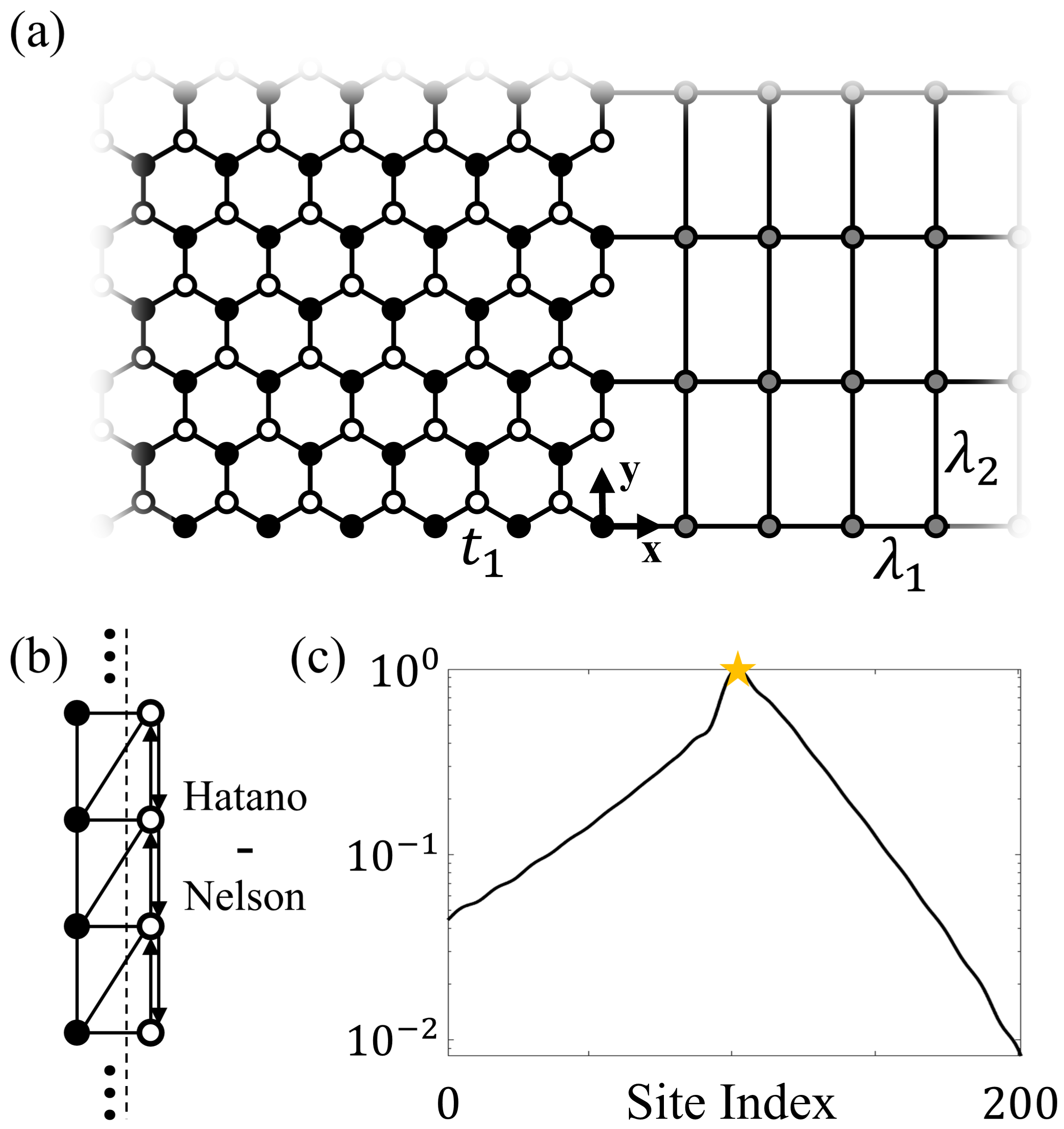
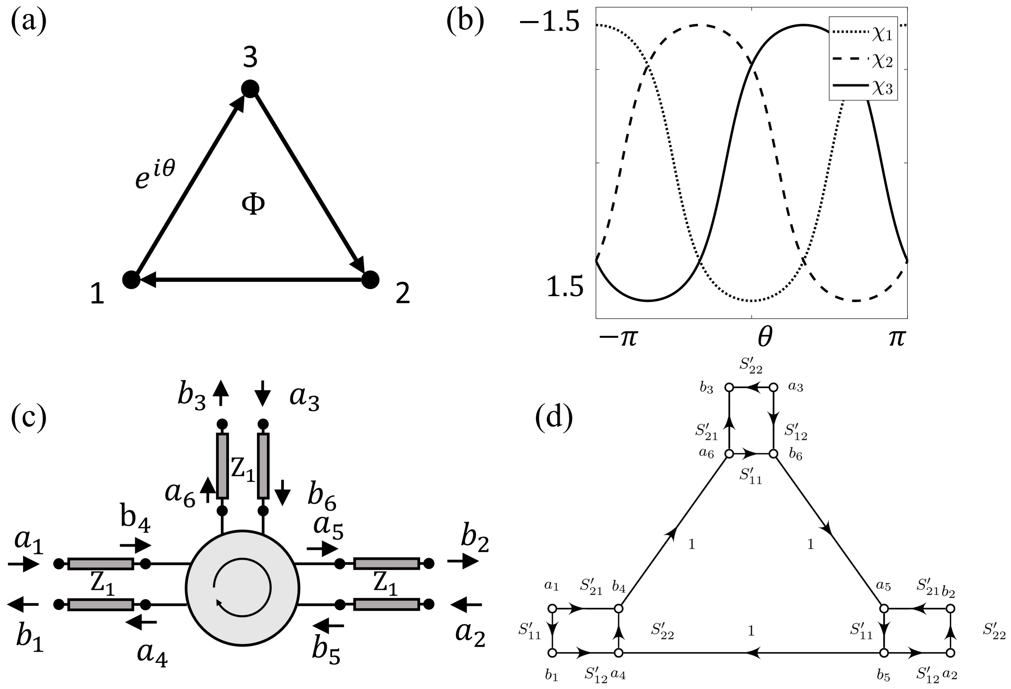
We consider a two-dimensional Chern insulator (CI) coupled to a conductor, and the line separates them (see Fig. 1a). The whole system is described by the Hamiltonian with hermiticity .
| (1) |
is the Hamiltonian of the Haldane model without breaking the inversion symmetry, and are the nearest and next-nearest neighbor hopping of the honeycomb sublattice (let’s denote the sublattice as and ), depending on the vectors along the two bonds. By referring to the phase diagram of the Haldane model, one can find is in the topological phase and the two bands are separated by , indicating the topological states in the gap. The Hamiltonian
| (2) |
describes the conductor with its band spanning . denotes the on-site energy and is the nearest neighbor hopping along of the square lattice.
| (3) |
gives the coupling on the interface.
Several cases are rather trivial or well-studied and hence been excluded here: (i) the excitation energy is in the conduction bands of CI and the conductor, the transport perpendicular to the interface is much like that between conductors; (ii) the excitation energy is in the conduction band of CI and the band gap of the conductor, the perpendicular transport is blocked; (iii) the energy is in their gaps, it’s well known that the transport along the interface is unidirectional and the number of the channel equals the Chern number [16, 17]. We consider the transport parallel to the interface when . In that case, can be reduced to the effective Hamiltonian for the edge states, and the reservoir assumption leads to that the effect of and can be replaced by the self-energy of the conductors [18, 19]. That is (more details see Appendix B)
| (4) |
where . Here, we represent in -momentum space by noticing the translation symmetry along -axis. but if hence the effective Hamiltonian of the interface is NH even though the whole system is Hermitian. Note that an extra eigenstate whose eigenvalue is zero appears in constructing , we need to drop it in the calculation.
It’s very hard to find a tight-binding chain lattice that corresponds to , so to give it an intuition, we consider the approximation model (e.g., ) around and set , and . Correspondingly,
| (5) |
where and . Figure 1b depicts the approximation tight-binding chain. The complex constant in the equation results in a global dissipation. By inspection, is nothing but the Hatano-Nelson model [20] describing the vortex pinning in superconductors. The hopping in this model is asymmetric, i.e. from site j to i while from site i to j, and ; it follows that the bulk states pile up at the boundary, namely, the NH skin effect. To describe the dispersion correctly, one needs to generalize to the complex domain [5, 21].
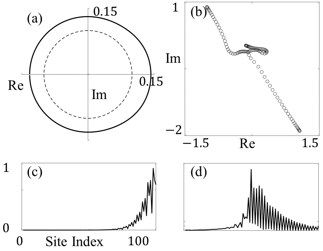
The response profile at the interface corresponding to an excitation is an indicator of the non-Bloch transport due to . If the chain eigenenergy and , the profile because of the skin effect. Inversely, if and , due to the dissipation (let the excitation at ). Therefore, in general cases, . So, the different decay (or growth) rates away from the excitation in the opposite direction indicate the non-Bloch transport.
The non-Bloch wave at the TI-conductor junction is universal. The reason is two-fold: (i) As part of the junction, the TI does not have to be the type of CI. The localized edge states make it possible to construct an effective one-dimensional system through the interface of two-dimensional materials. So, in principle, the CI (class A) used here can be replaced by other types of TI (e.g. class AII). In a separate work [22], we realize the NH skin effect at the interface between a time-reversal TI and a conductor; (ii) In contrast to Ref. [23], no extra requirement for the conductor is adopted here. In there, a relative momentum shift between the reservoir and the nanowire leads to asymmetric hopping. However, this asymmetry in our model results from the interaction between the unidirectional topological states and the reservoir self-energy.
III possible realization under reverse design
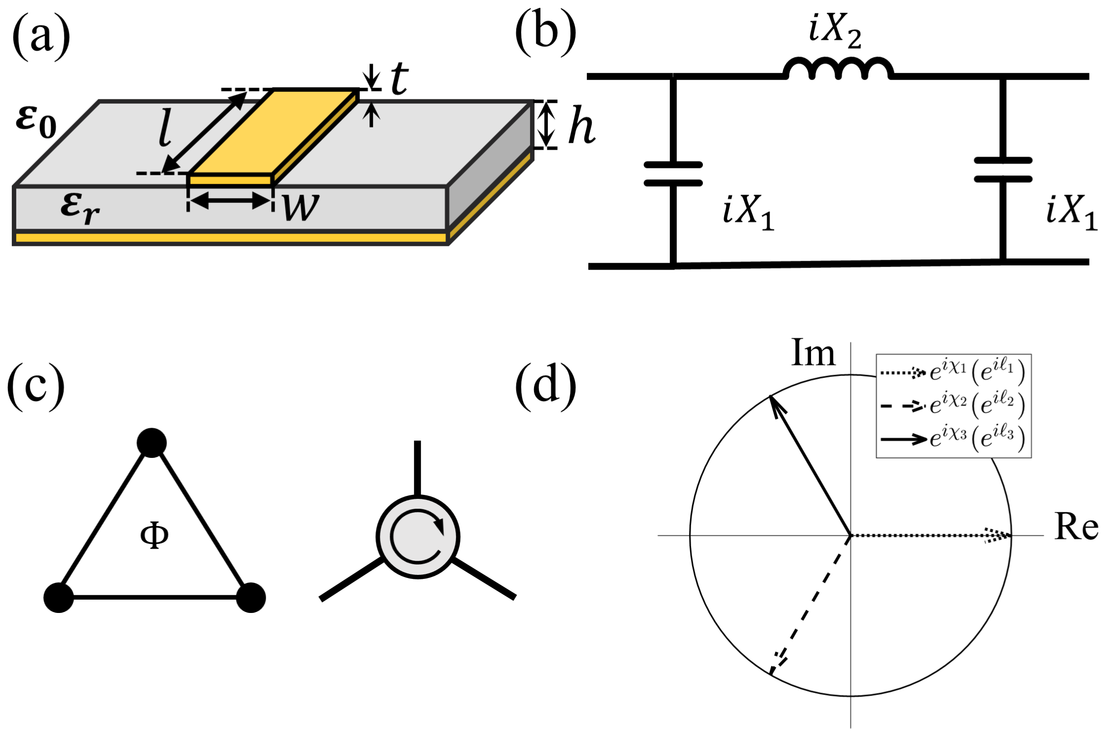
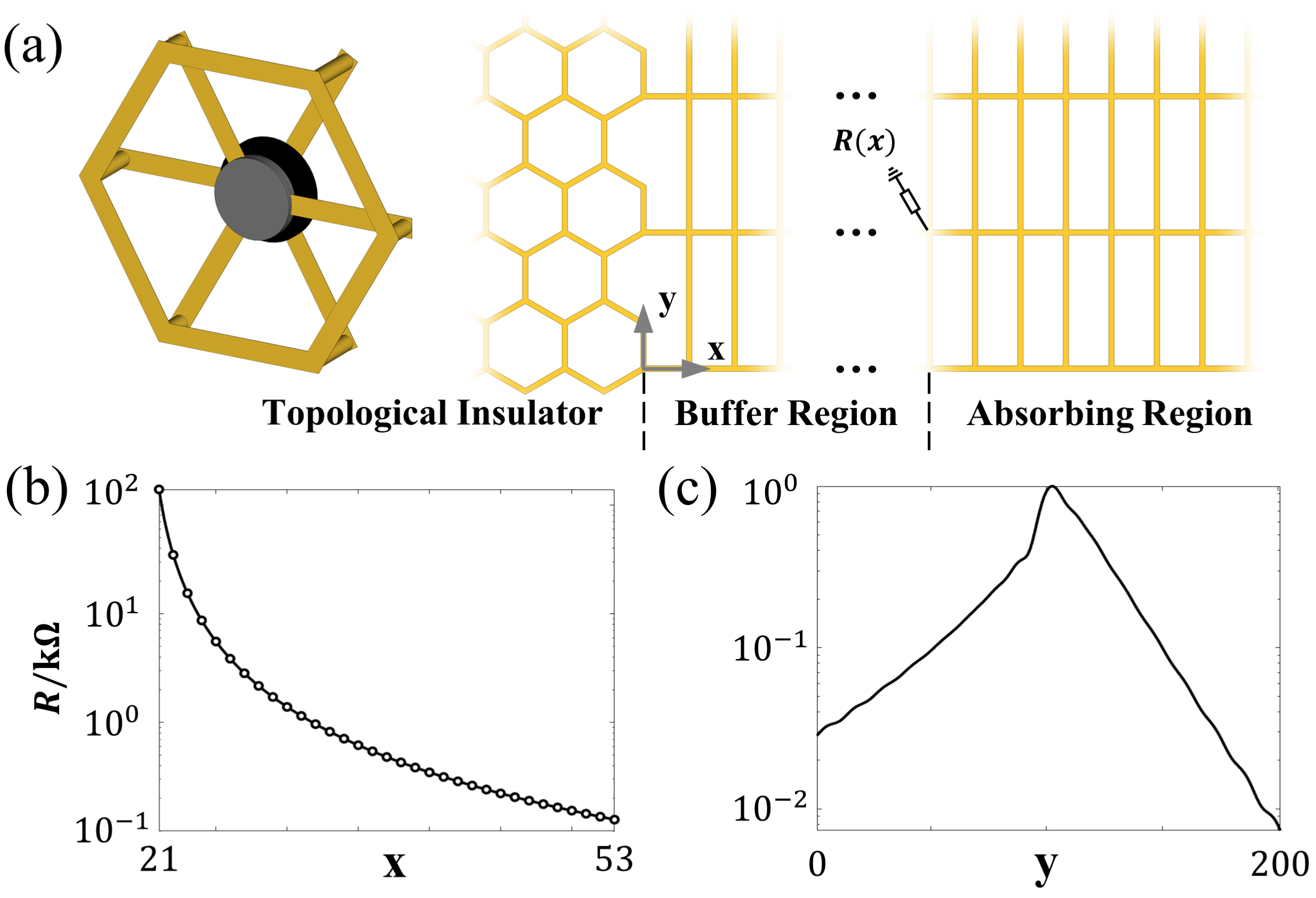
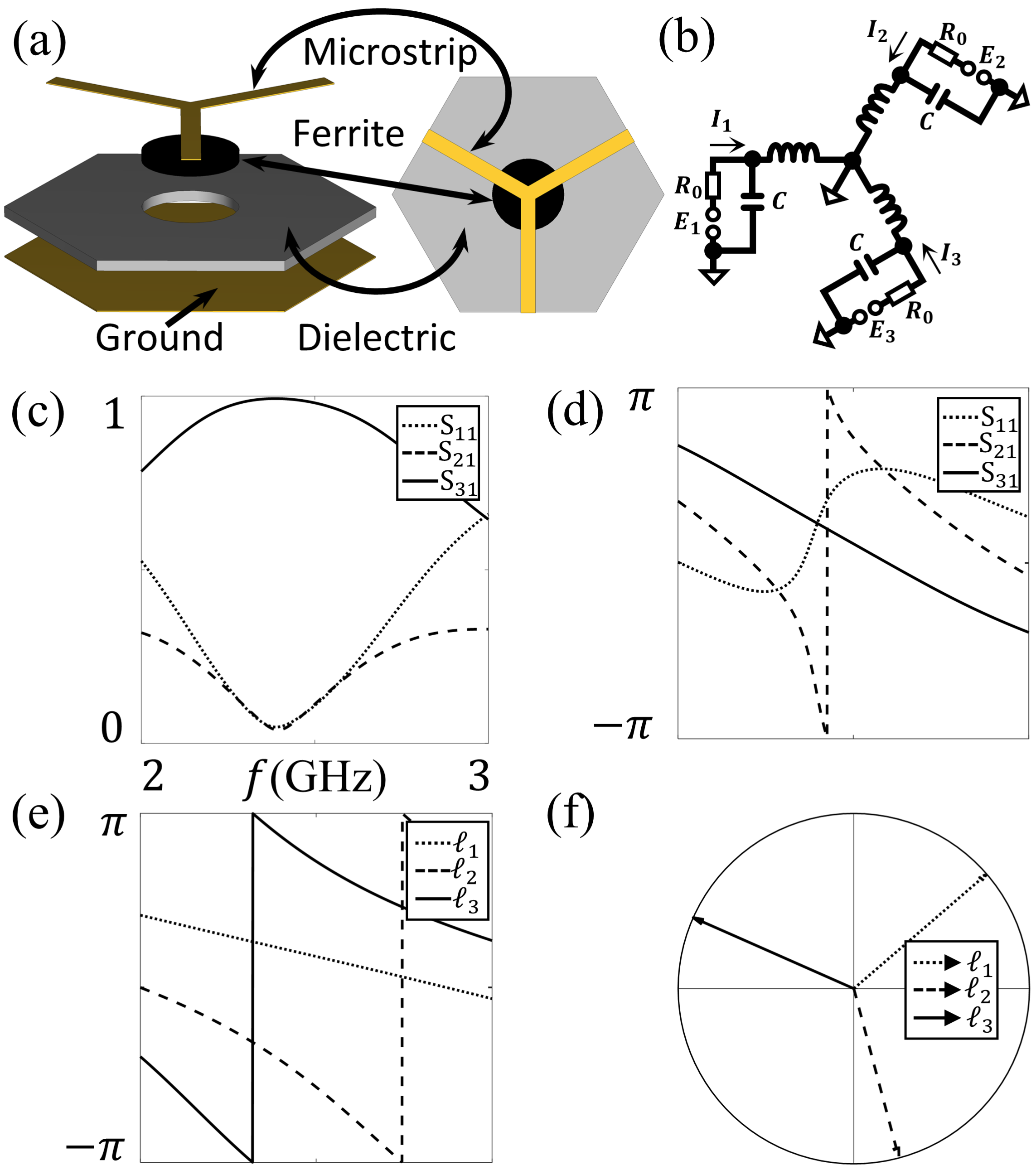
For the normal design procedure of topological metamaterials, one starts with some necessary parameters, such as lattice parameters, material parameters, unit cell structure, and so on; with those parameters, the dispersion relation of the metamaterials can be calculated with the help of the finite element simulation; if the band from the simulation is not topological, we tune the parameters and start over. That iterative procedure costs a huge of computing resources because of lack of generality, and the design may pose a challenge to sample fabrication (e.g., [24]). The starting point of the reverse design proposed here is the tight-binding model, and in principle, the design does not need the aid of finite element simulation. As a proof of concept, we illustrate this idea by realizing the junction mentioned above in the S band ( GHz) range, and the design scheme is readily generalized to the optical range.
First, consider the of Eq. 1 when (i.e., a graphene model). Implementing temporal topolectrical circuit (TTC) theory [25, 26], we can construct a circuit lattice with those correspondences, Halmiltonian admittance , eigenvalues self-admittance . The spirit of reverse design is that a waveguide with length (e.g., a microstrip line in Fig. 2a) is equivalent to a lumped circuit model (Fig. 2b). This equivalence enables one to ‘update’ a circuit lattice to a metamaterial in wave systems very effectively. More details about design including the graphene circuit, the converted waveguide metamaterial and its optimization can be found in Appendix F. Compared to the existing topolectrical circuits [27, 28], TTC is more suitable to be the starting point of the reverse design, because the impedance measurements required by existing circuits are out of reach in scattering experiments while scattering measurements are more accessible for electromagnetic metamaterials.
Next, we show how to introduce the next neighbor T-breaking hopping of which is critical to the Haldane model. It’s well-known this T-breaking term can be realized by nonreciprocal devices [29, 30, 31, 32], e.g., a RF circulator. In reality, a nonreciprocal device has very limited bandwidth, for example, the typical bandwidth is a few hundreds for a RF circulator working at , thus the frequency range of resonant-based metamaterials emulating the tight-binding Haldane model should be in this bandwidth. This frequency concern should not bother us since our TTC or TTC-based design operates at a fixed frequency and is not resonance-based. According to our previous works [25, 26], it looks like introducing the hopping can be easily achieved by finding out the admittance of the RF circulator, however, in general, the circulator does not have a well-defined admittance (Part 1 in Appendix E).
To solve that, let’s first understand the hopping in a geometric manner. Without loss of generality, we consider a minimal model containing three identical sites with hopping connecting them. The flux in the plaquette leads to a phase in , and the Hamiltonian is where are the Gell-Mann matrices. When , respects D3h symmetry, thus it has two-fold degeneracy eigenvalues. When pumping the flux, the symmetry is lifted down to C3, resulting in the splitting of the degeneracy (note that when with , respects D3h up to a gauge). So, we can use the frame of , with . Performing a bilinear transform, we have . is unitary: , and . So, in the frame of , characteristics uniquely specify the hopping relation between the sites (see Fig. 2d). On the other hand, compared to the admittance, the scattering-parameter of a circulator is always well-defined. In Appendix E, we demonstrate that three similar characteristics in a circulator uniquely determine the connectivity of the three nodes; this gives us an correspondence of T-breaking hopping between tight-binding models and the metamaterials (Fig. 2c): . In Appendix F, the simulation result establishes that the topological metamaterial designed under this correspondence supports the unidirectional edge state just as the Haldane model does.
Last, in the model of , we assume that the size of the conductor is semi-infinite such that it serves as a reservoir. The metamaterial construction of is similar to that of when , but it’s very cumbersome to prepare the sample in that size. Instead, one can reduce the semi-infinite geometry to a finite lattice with proper boundary condition, i.e., the perfect absorbing boundary condition using power-growth complex onsite potentials that completely absorb the incident wave (see Appendix G). The complex potentials are realized by grounding the nodes with resistances (see Fig. 3b). We remark that the boundary complex potential is not the origin of non-Bloch transport and the semi-infinite argument may also be mitigated by a fairly large lattice.
IV Outlooks
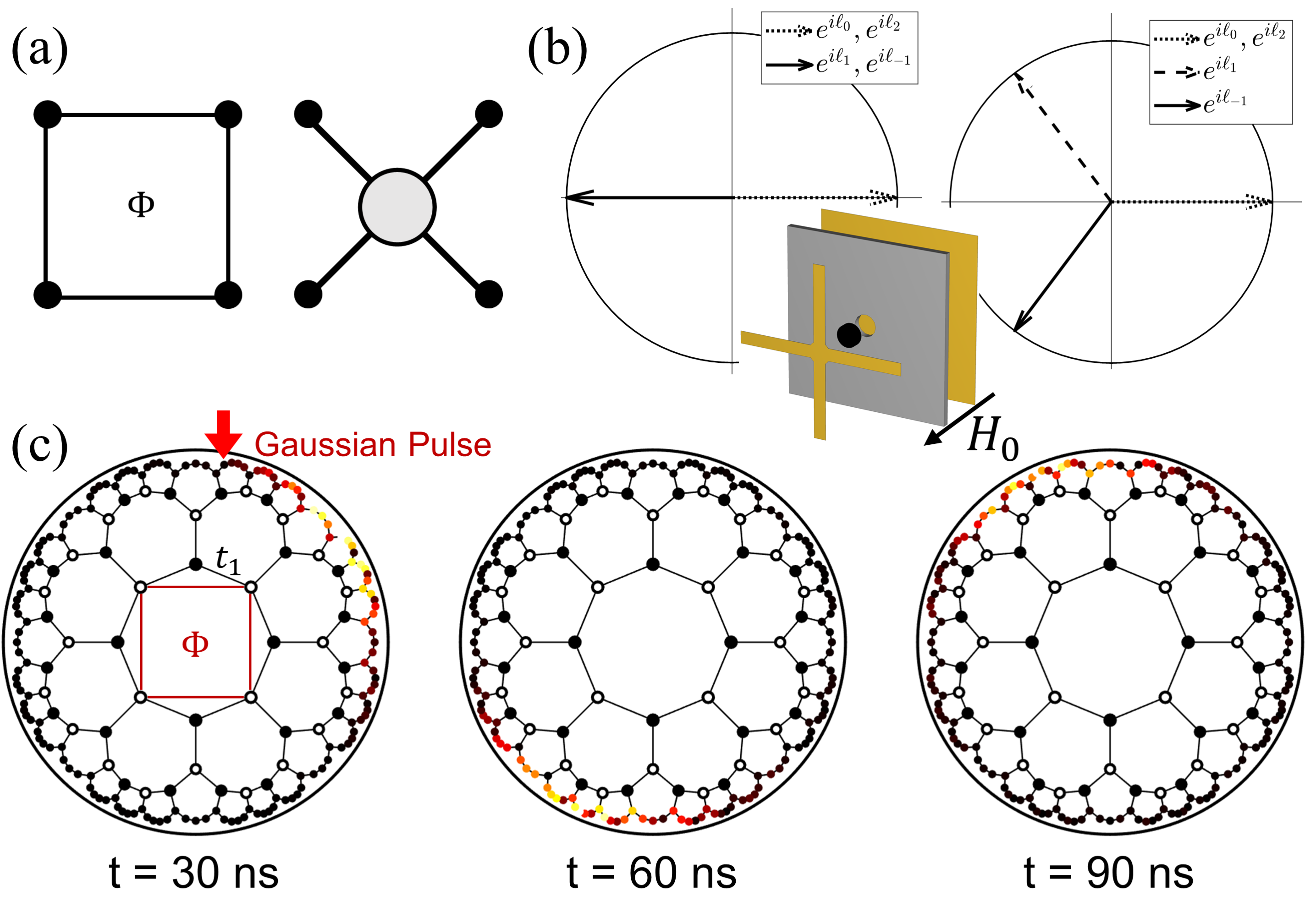
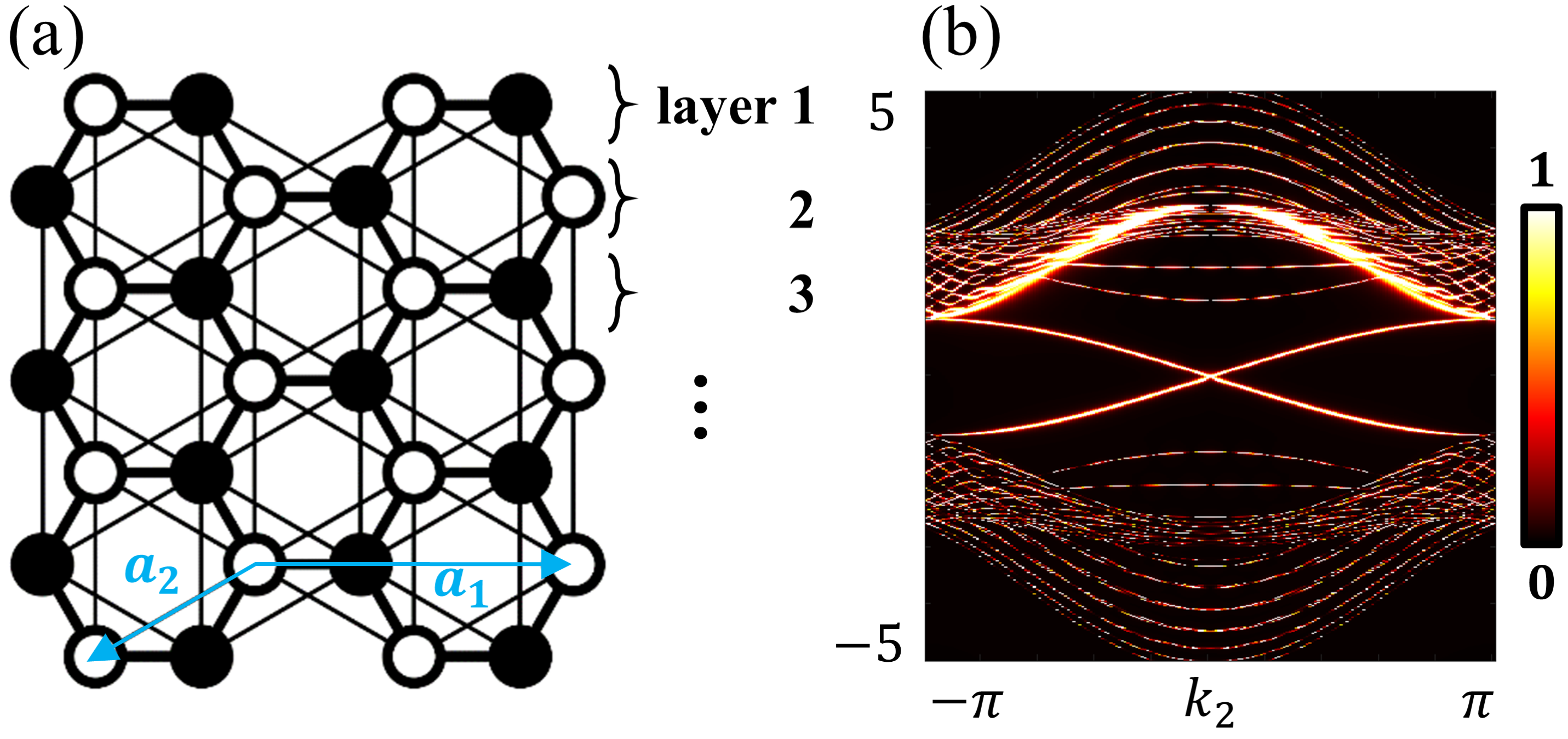
To show the great universalness of the reverse design, we would like to discuss its application in the hyperbolic lattice. Different from the normal lattice in the flat space or Euclidean space, the hyperbolic space [33, 34, 35, 36] is a tiling of the curved space with constant negative curvature. The curvature leads to the separated dimensions of position and momentum space, e.g., the tiling (in Schläfli notation) of the two-dimensional curved space has a four-dimensional Brillouin zone. This disagreement promises the band structure richer physics, such as non-Abelian bloch states [36] and topological phases [37]. Systems in the negatively curved space seem impossible to realize experimentally since the curved space can not be embedded in flat laboratory space. However, some works point out that electric circuits or waveguide resonators with the graph property can overcome this difficulty since the tight-binding models in the hyperbolic space only care about the nodes and the connectivity between nodes. However, there are still some obstacles for waveguide resonators, e.g., how to induce the model-requisite flux in broadband, and one may face a layout problem when two waveguides have to cross over each other.
Figure 4c illustrates the Haldane-like model with tiling in hyperbolic space. We set flux piercing the plaquette (Fig. 4a) formed by four sites hence . Two steps are taken to emulate the flux (Fig. 4b inset): (i) varying the ferrite diameter so that the unmagnetized disk resonates under eigenmodes. The field patterns lead to (Fig.4b left); (ii) applying a magnetic field will rotate in opposite directions while retaining the accident degeneracy (Fig.4b right). More details see Appendix E.5. Note that the device is not a four-port circulator. Bending the waveguide or increasing its physical length will not change its equivalent circuit as long as its electrical length is fixed. Above flexibility makes it possible to construct hyperbolic lattices on Euclidean substrates. The chiral edge state of the model is confirmed through the time evolution of a wave packet propagating clockwise along the boundary.
In summary, we provide an alternate approach to realize non-Hermitian systems in electromagnetics in a gain-free fashion. The reverse design procedure, i.e., the tight-binding modelstemporal topolectrical circuitselectromagnetic metamaterials, offers a prevalent paradigm to design the topological band of the metamaterials.
Acknowledgements.
We wish to acknowledge the support of the National Key Research & Development Program of China (Grant No.2023YFB3811400), National Natural Science Foundation of China (No. 52273296 and No. 51872154), Beijing Municipal Science & Technology Commission (No. Z221100006722016).References
- Miri and Alu [2019] M.-A. Miri and A. Alu, Exceptional points in optics and photonics, Science 363, eaar7709 (2019).
- Bender [2007] C. M. Bender, Making sense of non-hermitian hamiltonians, Reports on Progress in Physics 70, 947 (2007).
- Mostafazadeh [2002] A. Mostafazadeh, Pseudo-Hermiticity versus PT symmetry: The necessary condition for the reality of the spectrum of a non-Hermitian Hamiltonian, Journal of Mathematical Physics 43, 205 (2002).
- Bergholtz et al. [2021] E. J. Bergholtz, J. C. Budich, and F. K. Kunst, Exceptional topology of non-hermitian systems, Rev. Mod. Phys. 93, 015005 (2021).
- Yao and Wang [2018] S. Yao and Z. Wang, Edge states and topological invariants of non-hermitian systems, Phys. Rev. Lett. 121, 086803 (2018).
- Kunst et al. [2018] F. K. Kunst, E. Edvardsson, J. C. Budich, and E. J. Bergholtz, Biorthogonal bulk-boundary correspondence in non-hermitian systems, Phys. Rev. Lett. 121, 026808 (2018).
- Zhang et al. [2020] K. Zhang, Z. Yang, and C. Fang, Correspondence between winding numbers and skin modes in non-hermitian systems, Phys. Rev. Lett. 125, 126402 (2020).
- Feng et al. [2017] L. Feng, R. El-Ganainy, and L. Ge, Non-hermitian photonics based on parity–time symmetry, Nature Photonics 11, 752 (2017).
- El-Ganainy et al. [2018] R. El-Ganainy, K. G. Makris, M. Khajavikhan, Z. H. Musslimani, S. Rotter, and D. N. Christodoulides, Non-hermitian physics and pt symmetry, Nature Physics 14, 11 (2018).
- Konotop et al. [2016] V. V. Konotop, J. Yang, and D. A. Zezyulin, Nonlinear waves in -symmetric systems, Rev. Mod. Phys. 88, 035002 (2016).
- Ozawa et al. [2019] T. Ozawa, H. M. Price, A. Amo, N. Goldman, M. Hafezi, L. Lu, M. C. Rechtsman, D. Schuster, J. Simon, O. Zilberberg, and I. Carusotto, Topological photonics, Rev. Mod. Phys. 91, 015006 (2019).
- El-Ganainy et al. [2007] R. El-Ganainy, K. G. Makris, D. N. Christodoulides, and Z. H. Musslimani, Theory of coupled optical pt-symmetric structures, Opt. Lett. 32, 2632 (2007).
- Zhen et al. [2015] B. Zhen, C. W. Hsu, Y. Igarashi, L. Lu, I. Kaminer, A. Pick, S.-L. Chua, J. D. Joannopoulos, and M. Soljačić, Spawning rings of exceptional points out of dirac cones, Nature 525, 354 (2015).
- Rüter et al. [2010] C. E. Rüter, K. G. Makris, R. El-Ganainy, D. N. Christodoulides, M. Segev, and D. Kip, Observation of parity–time symmetry in optics, Nature Physics 6, 192 (2010).
- Groth et al. [2014] C. W. Groth, M. Wimmer, A. R. Akhmerov, and X. Waintal, Kwant: a software package for quantum transport, New Journal of Physics 16, 063065 (2014).
- Hasan and Kane [2010] M. Z. Hasan and C. L. Kane, Colloquium: Topological insulators, Rev. Mod. Phys. 82, 3045 (2010).
- Qi and Zhang [2011] X.-L. Qi and S.-C. Zhang, Topological insulators and superconductors, Rev. Mod. Phys. 83, 1057 (2011).
- Datta [1997] S. Datta, Electronic transport in mesoscopic systems (Cambridge university press, 1997).
- Bergholtz and Budich [2019] E. J. Bergholtz and J. C. Budich, Non-hermitian weyl physics in topological insulator ferromagnet junctions, Phys. Rev. Res. 1, 012003 (2019).
- Hatano and Nelson [1996] N. Hatano and D. R. Nelson, Localization transitions in non-hermitian quantum mechanics, Phys. Rev. Lett. 77, 570 (1996).
- Yokomizo and Murakami [2019] K. Yokomizo and S. Murakami, Non-bloch band theory of non-hermitian systems, Phys. Rev. Lett. 123, 066404 (2019).
- [22] In preparation, .
- Geng et al. [2023] H. Geng, J. Y. Wei, M. H. Zou, L. Sheng, W. Chen, and D. Y. Xing, Nonreciprocal charge and spin transport induced by non-hermitian skin effect in mesoscopic heterojunctions, Phys. Rev. B 107, 035306 (2023).
- Lu et al. [2013] L. Lu, L. Fu, J. D. Joannopoulos, and M. Soljačić, Weyl points and line nodes in gyroid photonic crystals, Nature Photonics 7, 294 (2013).
- Wu et al. [2023] M. Wu, Q. Zhao, L. Kang, M. Weng, Z. Chi, R. Peng, J. Liu, D. H. Werner, Y. Meng, and J. Zhou, Evidencing non-bloch dynamics in temporal topolectrical circuits, Phys. Rev. B 107, 064307 (2023).
- Wu et al. [2024] M. Wu, M. Weng, Z. Chi, Y. Qi, H. Li, Q. Zhao, Y. Meng, and J. Zhou, Observing relative homotopic degeneracy conversions with circuit metamaterials, Phys. Rev. Lett. 132, 016605 (2024).
- Lee et al. [2018] C. H. Lee, S. Imhof, C. Berger, F. Bayer, J. Brehm, L. W. Molenkamp, T. Kiessling, and R. Thomale, Topolectrical circuits, Communications Physics 1, 39 (2018).
- Imhof et al. [2018] S. Imhof, C. Berger, F. Bayer, J. Brehm, L. W. Molenkamp, T. Kiessling, F. Schindler, C. H. Lee, M. Greiter, T. Neupert, and R. Thomale, Topolectrical-circuit realization of topological corner modes, Nature Physics 14, 925 (2018).
- Wang et al. [2009] Z. Wang, Y. Chong, J. D. Joannopoulos, and M. Soljačić, Observation of unidirectional backscattering-immune topological electromagnetic states, Nature 461, 772 (2009).
- Yang et al. [2015] Z. Yang, F. Gao, X. Shi, X. Lin, Z. Gao, Y. Chong, and B. Zhang, Topological acoustics, Phys. Rev. Lett. 114, 114301 (2015).
- Hofmann et al. [2019] T. Hofmann, T. Helbig, C. H. Lee, M. Greiter, and R. Thomale, Chiral voltage propagation and calibration in a topolectrical chern circuit, Phys. Rev. Lett. 122, 247702 (2019).
- Zhang et al. [2021] Z. Zhang, P. Delplace, and R. Fleury, Superior robustness of anomalous non-reciprocal topological edge states, Nature 598, 293 (2021).
- Kollár et al. [2019] A. J. Kollár, M. Fitzpatrick, and A. A. Houck, Hyperbolic lattices in circuit quantum electrodynamics, Nature 571, 45 (2019).
- Boettcher et al. [2020] I. Boettcher, P. Bienias, R. Belyansky, A. J. Kollár, and A. V. Gorshkov, Quantum simulation of hyperbolic space with circuit quantum electrodynamics: From graphs to geometry, Phys. Rev. A 102, 032208 (2020).
- Maciejko and Rayan [2022] J. Maciejko and S. Rayan, Automorphic bloch theorems for hyperbolic lattices, Proceedings of the National Academy of Sciences 119, e2116869119 (2022).
- Lenggenhager et al. [2023] P. M. Lenggenhager, J. Maciejko, and T. c. v. Bzdušek, Non-abelian hyperbolic band theory from supercells, Phys. Rev. Lett. 131, 226401 (2023).
- Urwyler et al. [2022] D. M. Urwyler, P. M. Lenggenhager, I. Boettcher, R. Thomale, T. Neupert, and T. c. v. Bzdušek, Hyperbolic topological band insulators, Phys. Rev. Lett. 129, 246402 (2022).
- Alase et al. [2016] A. Alase, E. Cobanera, G. Ortiz, and L. Viola, Exact solution of quadratic fermionic hamiltonians for arbitrary boundary conditions, Phys. Rev. Lett. 117, 076804 (2016).
- Cobanera et al. [2017] E. Cobanera, A. Alase, G. Ortiz, and L. Viola, Exact solution of corner-modified banded block-toeplitz eigensystems, J. Phys. A: Math. Theor. 50, 195204 (2017).
- Alase et al. [2017] A. Alase, E. Cobanera, G. Ortiz, and L. Viola, Generalization of bloch’s theorem for arbitrary boundary conditions: Theory, Phys. Rev. B 96, 195133 (2017).
- Kaladzhyan and Bena [2019] V. Kaladzhyan and C. Bena, Obtaining majorana and other boundary modes from the metamorphosis of impurity-induced states: Exact solutions via the t-matrix, Phys. Rev. B 100, 081106 (2019).
- Pinon et al. [2020] S. Pinon, V. Kaladzhyan, and C. Bena, Surface green’s functions and boundary modes using impurities: Weyl semimetals and topological insulators, Phys. Rev. B 101, 115405 (2020).
- Hatsugai [1993] Y. Hatsugai, Chern number and edge states in the integer quantum hall effect, Phys. Rev. Lett. 71, 3697 (1993).
- Dwivedi and Chua [2016] V. Dwivedi and V. Chua, Of bulk and boundaries: Generalized transfer matrices for tight-binding models, Phys. Rev. B 93, 134304 (2016).
- Mong and Shivamoggi [2011] R. S. K. Mong and V. Shivamoggi, Edge states and the bulk-boundary correspondence in dirac hamiltonians, Phys. Rev. B 83, 125109 (2011).
- Wimmer [2009] M. Wimmer, Quantum transport in nanostructures: From computational concepts to spintronics in graphene and magnetic tunnel junctions, Phd thesis, University of Regensburg, Regensburg (2009).
- Lee and Joannopoulos [1981] D. H. Lee and J. D. Joannopoulos, Simple scheme for surface-band calculations. ii. the green’s function, Phys. Rev. B 23, 4997 (1981).
- Youla et al. [1959] D. Youla, L. Castriota, and H. Carlin, Bounded real scattering matrices and the foundations of linear passive network theory, IRE Transactions on Circuit Theory 6, 102 (1959).
- Helszajn [1973] J. Helszajn, Waveguide and stripline 4-port single-junction circulators (short papers), IEEE Transactions on Microwave Theory and Techniques 21, 630 (1973).
- Helszajn et al. [2004] J. Helszajn, M. McKay, and I. Macfarlane, Complex gyrator circuit of 4-port single junction circulator, IEEE microwave and wireless components letters 14, 40 (2004).
- Helszajn [1970] J. Helszajn, The adjustment of the m-port single-junction circulator, IEEE Transactions on Microwave Theory and Techniques 18, 705 (1970).
- Weston and Waintal [2016] J. Weston and X. Waintal, Linear-scaling source-sink algorithm for simulating time-resolved quantum transport and superconductivity, Phys. Rev. B 93, 134506 (2016).
- Kloss et al. [2021] T. Kloss, J. Weston, B. Gaury, B. Rossignol, C. Groth, and X. Waintal, Tkwant: a software package for time-dependent quantum transport, New Journal of Physics 23, 023025 (2021).
Appendix A A review about self-energy
A.1 Junction
Let us first give the topological junction an intuition. Assuming each side of the junction is described by a Hermitian Hamiltonian, and , and the two sides are coupled through some surface mechanism, such as the chemical bonds. Then the junction is Hermitian and the total Hamiltonian can be written as.
| (6) |
where denotes the coupling. Correspondingly, the retarded green function can be defined as or
| (7) |
When one of the sides is so “large”, say the side described by , that the effect of on is negligible. In this case, constitutes a reservoir or the environment. After some simple algebra, we can find the Green’s function of the smaller side is expressed as , where is the so called self-energy and the effect of on is encoded with it. So the effective Hamiltonian of the smaller side is , and in general is non-Hermitian owing to the complexity of . Note that the non-Hermitisity is introduced without any gain or loss, while the gain and loss are essential in optical realization. The concept of self-energy is widely applied in physics, such as those coming from the electron-electron/phonon Coulomb interactions, the impurity scattering and the interaction with the reservoir (considered here), although their physical origins may differ.
A.2 Reservoir argument
In the main article, we realize an effective NH system by considering two coupled subsystems. The self-energy treatment requires that one of the subsystems can be viewed as the reservoir. Here we show that self-energy is out of the capability to delineate two comparable coupled subsystems.
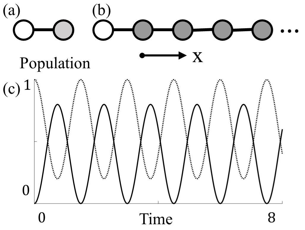
Let’s consider two comparable coupled subsystems with only one state in each (Fig. 5a). The whole system is described by
| (8) |
and are creation and annihilation operator in subsystem I respectively, and in subsystem II. Now if we are interested primarily in I, the effect of II through a self-energy is
| (9) |
However, II is not a reservoir in the common sense. The fundamental feature of a reservoir is that the rate constant for outflow or inflow (e.g., heat flow, current flow) remains unaffected by the filling and vacuuming of states and other dynamical details [18]. II does not satisfy this criterion because the escape rate is
| (10) |
which is affected strongly by (a proper reservoir should be independent of ). This means that rate out of I is affected by the rate into it. By using the von-Neumann equation we could calculate the populations of desity matrix as a function of time. The system is then driven between subsystems, and the populations present Rabi oscillations with frequency , as is shown in Fig. 5c.
Now consider two coupled subsystems with the subsystem II consisting of states (e.g., a chain with sites, see Fig. 5b), the resulting Hamiltonian is
| (11) |
The eigenenergies of II are given by and the corresponding normalized wavefunction is , where . So, the effect of II through the self-energy is
| (12) |
When , convert the summation to an integral:
| (13) |
and we have (we set for simplicity). The escape rate is . By contrast, the reservoir II with states has a constant escape rate independent of .
Appendix B Edge state Hamiltonian
There are several ways to calculate the exact solutions of the edge states, such as via extending Bloch’s theorem [38, 39, 40], the impurity Green’s function [41, 42], the transfer matrix [43, 44], the geometric algebra [45] and so on. The difficulty for the Haldane model roots in the next-nearest neighbor hopping. Here, we follow the approach using the Green’s function [45]. The calculation is summarized as follows: we begin with a model with fully periodic boundary conditions, which allows us to write down the Hamiltonian in the momentum space; next, we add hopping perturbation that substrate the interaction crossing the first row and the end row of the lattice, forming an open boundary along that direction; the final Green’s function of the resulting system is given by the Dyson equation, and the poles of it enable the analytic solution of the edge states. Note that the geometric algebra method can not be applied here since the next-nearest neighbor hopping appears and the supercell Hamiltonian (e.g., two unit cells) is not of Dirac form.
B.1 Green’s function with periodic boundaries
After Fourier transform, the Haldane model of Eq. 1 (, Fig. 6a) can be expressed in a compact form as , where
| (14) |
And the spectrum of the model is . Correspondingly, the Green function in space is
| (15) |
To include the hopping perturbation, we keep the momentum coordinate but perform an inverse Fourier transform to write down the Green’s function in real-space coordinate in the direction. Thus, we have
| (16) |
where
| (17) |
and with . is a -by- block matrix.
B.2 Hopping perturbation
Hopping perturbation deletes the hopping crossing the first row and the end row of the lattice, such that it creates two edges perpendicular to . Its explicit expression is
| (18) |
where
| (19) |
() describes the nearest (next-nearest) neighbor hopping between the layers along .
B.3 Green’s function with the perturbation
The Dyson equation gives the full Green’s function in terms of the initial Green’s function and the hopping perturbation , that is
| (20) |
The has no poles in the gap, so the poles of , alternatively the zeros of , are the edge state eigenvalues when . To show that, we numerically calculate the local density of states given in general by (see Fig. 6b). Taking the ansatz of edge state wave vector and substituting 16 and 18 into 20, we have
| (21) |
The ellipses indicate the non-zero subblock. localizes at the first layer and the promises the localization. And,
| (22) |
which together require (Kramer criterion)
| (23) |
It can be further simplified by a decomposition in terms of triangular matrices (note that ),
| (24) | |||||
So, we can calculate the edge state spectrum explicitly by solving . The edge states energy is given by with , and () corresponds to the state localized at the first (last) layer.
B.4 Edge state wave vector
We can also calculate the through Eq. 22. A more convenient method is by extending Bloch’s theorem. In our case, we extend the to the complex domain with an analytic continuation, and we have with . Then the secular equation gives . With , has the form
| (25) |
where the argument is suppressed. The normalized solution to this equation is .
Finally, we can use the edge state projector to construct the effective edge Hamiltonian
| (26) |
Another normalized solution with respect to , i.e., state locolized at the last layer, is . Taking two edge states together, the effective Hamiltonian is
| (27) |
It’s very interesting that is equivalent to the Su-Schrieffer-Heeger model.
Appendix C Self-energy
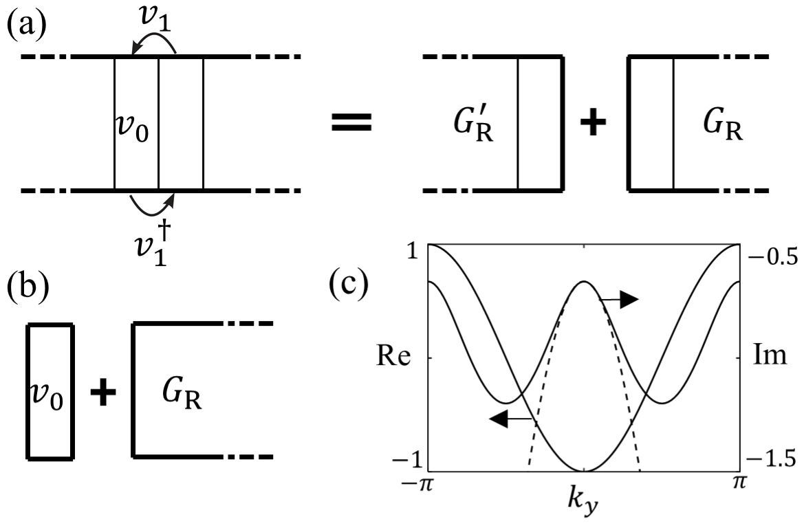
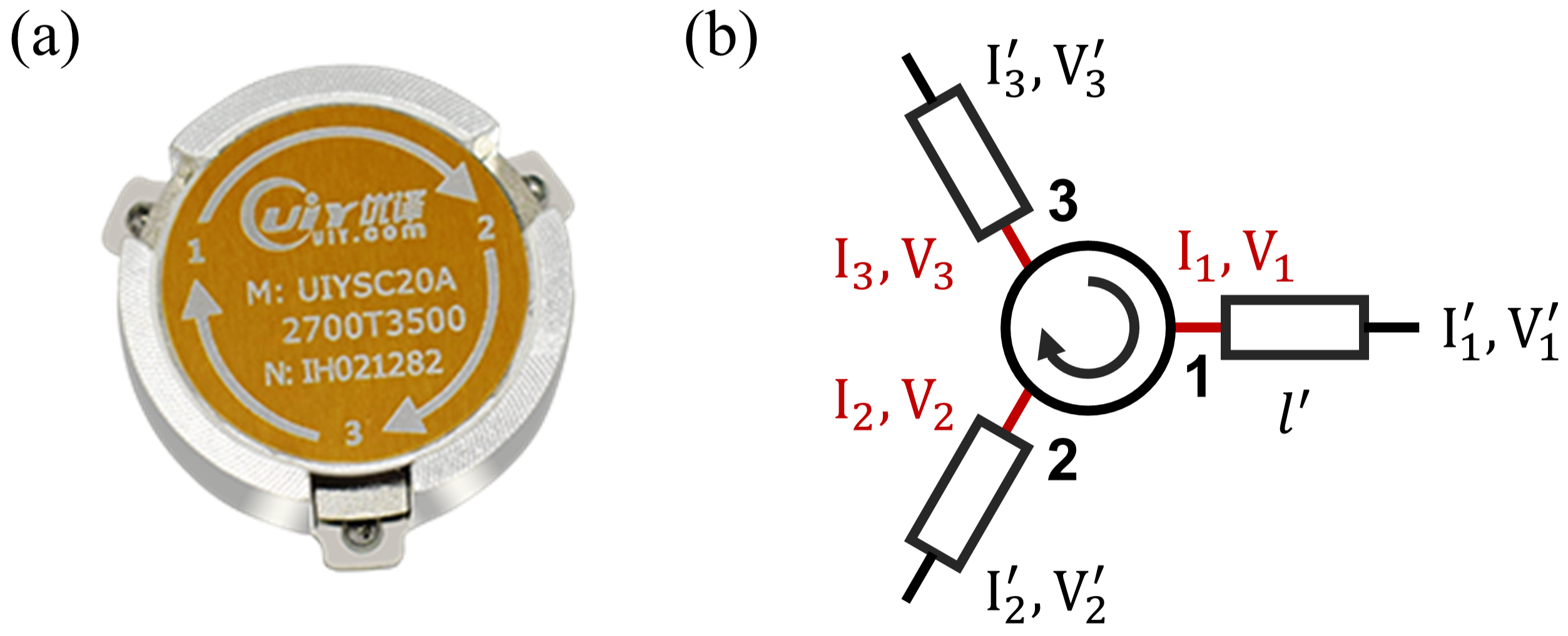
The formal expression to evaluate the self-energy is , where represents the surface Green’s function and is the coupling between the closed system and the reservoir. A stable algorithm based on the Schur decomposition (as well as the conventional method using the eigendecomposition) to calculate can be found in Ref. [46]. Here, we follow the procedure using the transfer matrix [47].
Constructing blocks from the reservoir lattice, so that the system is periodic in those blocks and the hopping between them is restricted to the nearest neighbor, as shown in Fig. 7a. In terms of those blocks, we have the recursion relation of subblock matrix of the Green’s function
| (28) |
which can be rewritten as
| (29) |
The above expression requires is nonsingular. If it is singular, refer to Ref. [44]. Then surface Green’s function is obtained from
| (30) |
or
| (31) |
or depends on which semi-infinite part one is interested in (Fig. 7a). is the subblock of the matrix whose column vectors are ordered eigenvectors of , i.e.,
| (32) |
corresponds to the eigenvalue and corresponds to the eigenvalue respectively. In general, they are not independent and are related by a symmetry (e.g., inversion symmetry).
The self-energy has a very simple form if one notices the semi-infinite reservoir does not change upon adding another block . With , the Green’s function on the additional block is
| (33) |
Compare with Eq. 30, we have .
Appendix D Response profile
Here, we give some simple examples to illustrate the response profile, which is an indicator of non-Bloch transport. The model is the Hatano-Nelson model under the open boundary condition:
| (35) |
where we add the global complex onsite potentials . Henceforth we set the nearest neighbor hopping parameter to unity.
-
•
Hermitian case: and . The response profile corresponding to a excitation is shown in Fig. 8b, and the excited Bloch wave propagates without attenuation.
-
•
NH case with a global dissipation: and , the eigenvalues of are in the complex domain owing to , but does not lead to NH skin effect. As shown in Fig. 8c, the attenuation shows no inclination to the propagation orientation, thus the response profile corresponding to a excitation is , whcih consists with our intuition of wave attenuation owing to the loss.
-
•
Pseudo-Hermitian case with skin effect: and , the eigenvalues of are all real numbers due to pseudo-Hermiticity . The eigenstates pile up at the boundary, exhibiting NH skin effect. The response profile corresponding to a unit excitation is shown in Fig. 8d, and the profile because of the skin effect.
-
•
NH case with both the skin effect and the global dissipation: and . Figure 8e shows the calculated response profile, which is roughly . The dacay (or growth) rate is orientation-dependent under the competition between skin effect and global dissipation.
Figure 9 shows some calculated results of the effective chain model (see text around Eq. 5 in the main text).
Appendix E Realization of the hopping with a phase
Our previous works [25, 26] develop a correspondence between circuit networks and tight-binding lattice models. We want to apply this theory to higher-frequency regions, such as radio and optical frequencies. Higher frequencies imply decreasing wavelengths. This follows that voltages and currents no longer remain spatially uniform when compared to the geometric size of the discrete circuit elements. As a consequence, they have to be treated as propagating waves. Since Kirchhoff’s voltage and current laws do not account for these spatial variations, we must significantly adjust the analysis from conventional lumped to distributed circuit representation.
Multiple port networks are essential tools in restructuring and simplifying complicated circuits as well as in providing key insight into the performance of devices. To describe such network input-output parameter relations, we have impedance, admittance, S-parameter, hybrid, and ABCD parameters–conversions exist between these sets. However, some relations may not be well-defined, such as the admittance of a circulator (see subsection 1), causing difficulty in finding the correspondence between higher-frequency networks and tight-binding lattice models. The principal advances of the S-parameter are that: (i) it is always well-defined in a passive device; (ii) the experimental determination of it is convenient without the need to know the internal structure of the device. Here, we show how to realize the hopping with a phase (we set the coupling amplitude to unity) in the TTC network by designing the S-parameter (see subsection 2-4) when the admittance of the device is not available. The phased-hopping breaks the reciprocity, i.e., , so we use a circulator to realize this hopping. The ‘black box’ treatment of the S-parameter indicates that distinct devices or different network configurations can realize the same phased-hopping since they may have an identical S-parameter (see subsection 4). The calculation of S-parameters is based on the signal flow graph, subsection 2 will provide some context.
E.1 Ill-defined admittance of microwave circulators
The circulator geometry (Fig. 10a) can readily be analyzed using the lumped element configuration (Fig. 10b illustrates the network). The usual arrangement consists of a ferrite disk with three strips wound on it: i) the strips are oriented at with respect to each other and are electrically short at the end of them; ii) a direct magnetic field is applied normal to the plane of the circulator, so the relative permeability tensor of the ferrite disk is
| (36) |
with
| (37) |
, and , where is the saturation magnetization, is the gyromagnetic ratio, is the demagnetizing factor. The presence of imaginary off-diagonal components having opposite signs in is the basis for the nonreciprocal effect.
The energy within the disk is essentially magnetic because of shorted strips. That follows that the simplified equivalent circuit in the disk, which retains all of the electrical characteristics, contains three mutual inductances. Shunt capacities out of the disk are added to maintain the characteristic impedance. So, the voltage–current relationships (impedance) at the terminals of the disk structure are
| (38) |
Note that as .
The admittance of the circulator, which is the inverse of , is ill-defined since its impedance is singular (i.e., the voltages do not determine the currents). Nevertheless, we can calculate the pseudoinverse of ,
| (39) |
One can hardly find any correspondence to .
The scattering matrix however is well-defined (note that every passive circuit has a scattering matrix [48]), and if the network is dissipationless. The circulator respects C3 symmetry, thus we can use the frame defined in the main text to diagonalize the matrix, . This also follows that , and . Similarly, the eigenvalues uniquely define the scattering relation between ports.
Figure 10c and d show the scattering parameters of the circulator and its characteristics as frequency varies. At the resonant frequency of the circulator, the scattering matrix is approximate to an ideal circulator:
| (40) |
and the characteristics are .
E.2 Review of signal flow graphs
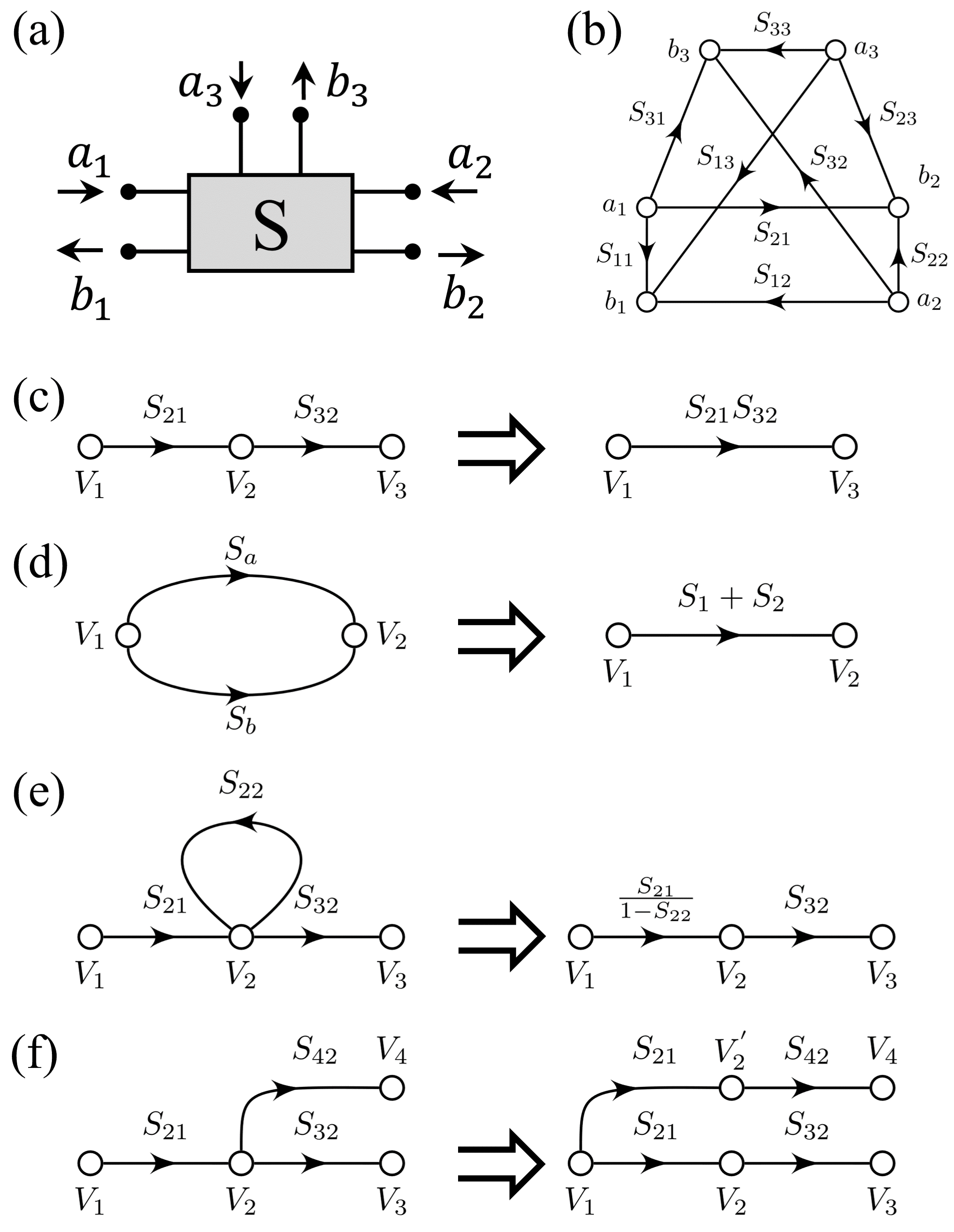
The analysis of networks is greatly facilitated through signal flow graphs. The primary components of the graph are nodes and branches. Each port of a network has two nodes: node is deployed to indentify a entering wave, while a reflected wave. A branch is a directed path between two nodes representing signal flow from one node to another. The S-parameter (the scattering matrix, e.g., Fig. 11a and b) is defined as
| (41) |
In the network, we use the normalized incident power wave and reflected power wave :
| (42) |
where the is the characteristic impedance of the connecting waveguide on the input and output side of the network. In what follows, we set for simplicity. A signal flow graph can be reduced to a single branch between two nodes using the four basic decomposition rules to obtain any desired wave amplitude ratio (Fig. 11c-f).
E.3 Two sites
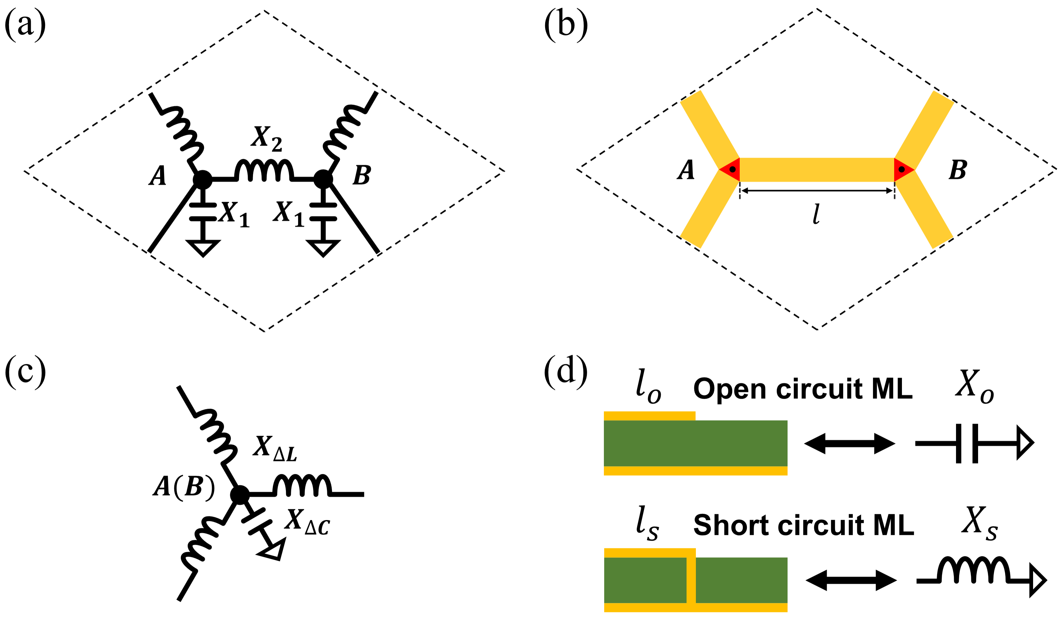
We employ a three-port ideal circulator (we set in Eq. 40 ) to realize the two-site coupling with an arbitrary phase and set the coupling amplitude to unity. The Hamiltonian of the two sites reads
| (43) |
The bilinear transform gives . One can not find a -independent frame that diagonalizes the transformed matrix, but we can define two characteristics as by noting the off-diagonal form of the transformed matrix.
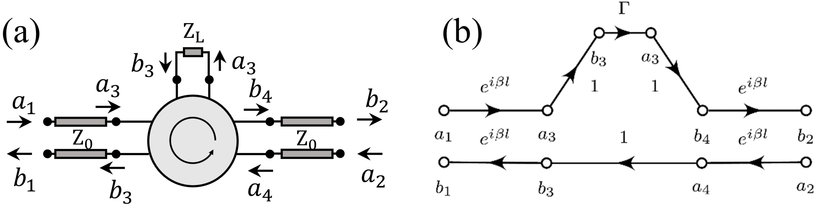
Two ports of the circulator are attached to the waveguides with electrical length , where is the wavenumber in the waveguide and is the physical length of the waveguide, and the rest port is terminated in a load impedance . Using the flow graph Fig. 12b, the S-parameter of this configuration is
| (44) |
where is the reflection coefficient. Unitary matrix leads to . Similarly, we can define the characteristics of as is and . and give us the correspondence, for example, when , , . Note that the load can be realized by a piece of waveguide with its end grounded or open (see Fig. 16 and text around there).
E.4 Three sites
Here, we show how to realize the next-nearest neighbor hopping required in the Haldane model. To illustrate it, consider the following three-site Hamiltonian (Fig. 13a):
| (45) |
The transformed matrix can be diagonalized by the frame because of the C3h symmetry: , where , with . The characteristics are shown in Fig. 13b as varies.
To realize that, we employ a three-port circulator with its ports attached to waveguides, see Fig. 13c. The waveguides attached have the characteristic impedance of , and the electrical length is . Using the flow graph Fig. 13d, the S-parameter of this configuration is
| (46) |
and , and due to C3 symmetry of the configuration (i.e. is a cicular matrix denoted as ). is the scattering matrix because of the impedance mismatch between connecting waveguides of and attached waveguides of , . The mirror symmetry of the impedance-mismatch scattering leads to and follows from . The characteristics of S-parameter (i.e., the eigenvalues of the S-parameter) and characteristics of transformed-matrix give the correspondence, for example, when , , .
E.5 Four sites
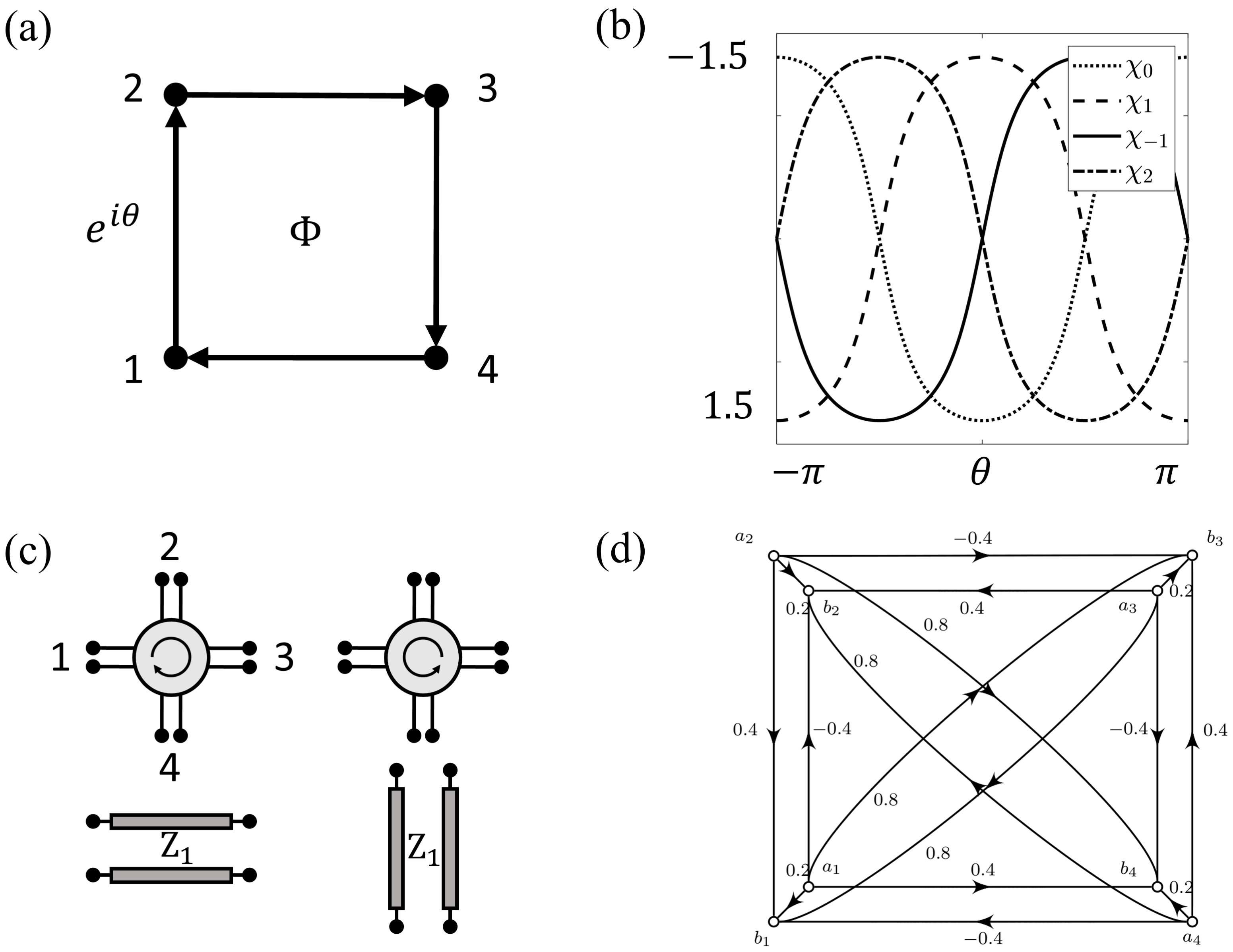
Here, we show how to introduce the flux through a four-site plaquette. Without losing generality, we set the coupling amplitude to be unity and the onsite potential to be zero (Fig. 14a). The resulting Hamiltonian is
| (47) |
When , the model respects D4h symmetry, So according to group theory, we can generate the equivalence representation (i.e., transform between equivalent sites) for the symmetry. In this case, the equivalence representation is reducible:
| (48) |
where , and denote the unreducible representation of D4h. is a 2-by-2 matrix, meaning that two of the four eigenvalues of are degenerate. Those two-fold eigenvalues can be lifted by pumping flux , and respects C4 symmetry when pumping. So we can use a symmetrical set of basis
| (49) |
Under this frame , the transformed matrix can be diagonalized as . Those characteristics are shown in Fig. 14b as varies.
One of the simplest ways to realize is by taking advantage of two-site couping (see text around Eq. 43). Here, we introduce the other two ways. Without losing generality, we set in the following.
I—If the S-parameter shares the same characteristics as , will take the form . when . We can decompose into several channels, where , ,
| (50) |
By inspection, we find that and are nothing but the S-parameters of four-port right-hand and left-hand circulators. or corresponds to the reciprocal scattering between port-1 and port-3 or scattering between port-2 and port-4 (Fig. 14c). This construction can be easily verified by the sigal flow graph shown in Fig. 14d.
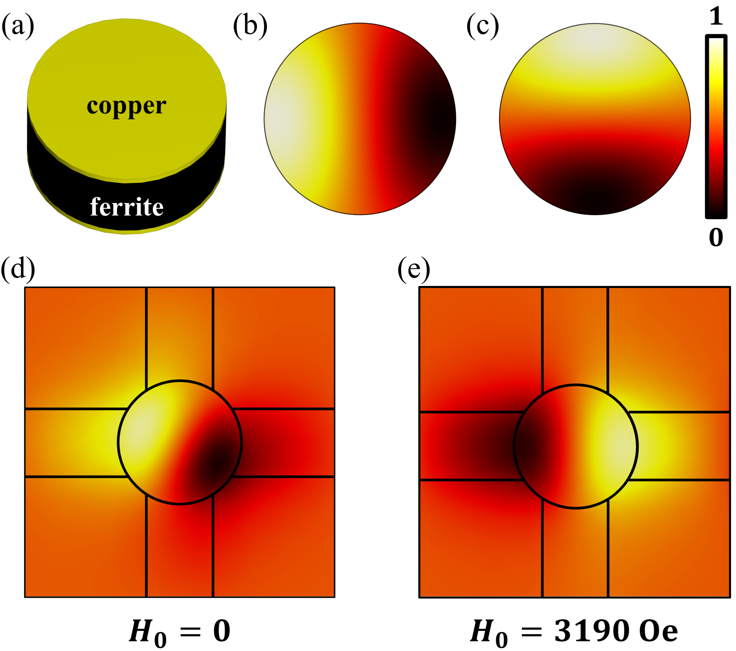
II— The above realization is still cumbersome for experiments. The construction discussed here is based on the ferrite eigenvalue adjustment for the 4-port nonreciprocal devices [49, 50, 51]. The geometry of a dielectric disk is shown in Fig. 15a. Here, we focus on the resonant modes supported by the disk. Without the external magnetic field, two modes are degenerate due to the cylinder symmetry of the disk, and their field patterns resemble the and orbitals of an atom (Fig. 15b and c). If we attach four ports to this disk under the C4 symmetry (e.g., inset of Fig. 4b in the main text), the S-parameter between ports around the eigenfrequency is . This follows that the excitation from one port only excites one mode of . For example, excitation from port 1 can only excite mode, so it only couples to port 3, and there is no cross-over between channel and channel (Fig. 15d).
Correspondingly, the characteristics of are (Fig. 4b left in the main text), because of the D4h symmetry, because of the accidental degeneracy. Those characteristics can be adjusted by the amplitude of the direct magnetic field. This adjustment rotates the standing wave formed by to make sure (Fig. 15e), and it lifts the degeneracy of and without affecting and (Fig. 4b right in the main text).
Appendix F Simulations of microstrip line metamaterials
This section gives the details about simulations of the metamaterials. Firstly, we use microstrip line (ML) to demonstrate the flexibility of TTCs to upgrade to higher frequencies. The ML circuit also exhibits the property of momentum resolution, which is the advantage of TTCs. Moreover, in order to construct Haldane model with ML, we analyze the admittance properties of a circulator.
F.1 Upgrade of TTCs
To construct the topological junction, we first consider the graphene lattice with only the nearest neighbor hopping and onsite potential , which is the basis of the Haldane model. The Hamiltonian of such lattice reads
| (51) |
and can be realized with temporal topolectrical circuits (TTCs). The unit cell of the corresponding circuit lattice is shown in Fig. 16a. The distance between the sublattices and is set to be 1. Thus, the lattice constant is and the admittance matrix in momentum space reads
| (52) |
where is the operating angular frequency and is the n-by-n identity matrix. Generally, the nearest neighbor hopping is realized with the inductor and the onsite potential is adjusted through the grounded capacitor .
As stated in the main text, TTCs can be upgraded to the microwave domain. Such upgrade is practical for many platforms, e.g., waveguide, coaxial line, ML and so on, and we use ML to illustrate the procedure. ML consists of a dielectric substrate with a conductor strip attached to its surface and the ground plane on the other. Under a certain parameter range, the electromagnetic properties of an ML with width and length are equivalent to a pi-shaped circuit as shown in Fig. 2a and 2b. The admittances of the components are
| (53) |
where is the characteristic impedance and is the wave number. The ML parameters are mm, , mm, mm, , GHz, which lead to the impedance and the electrical length . Thus, , the self-admittance of both site and is equal to .
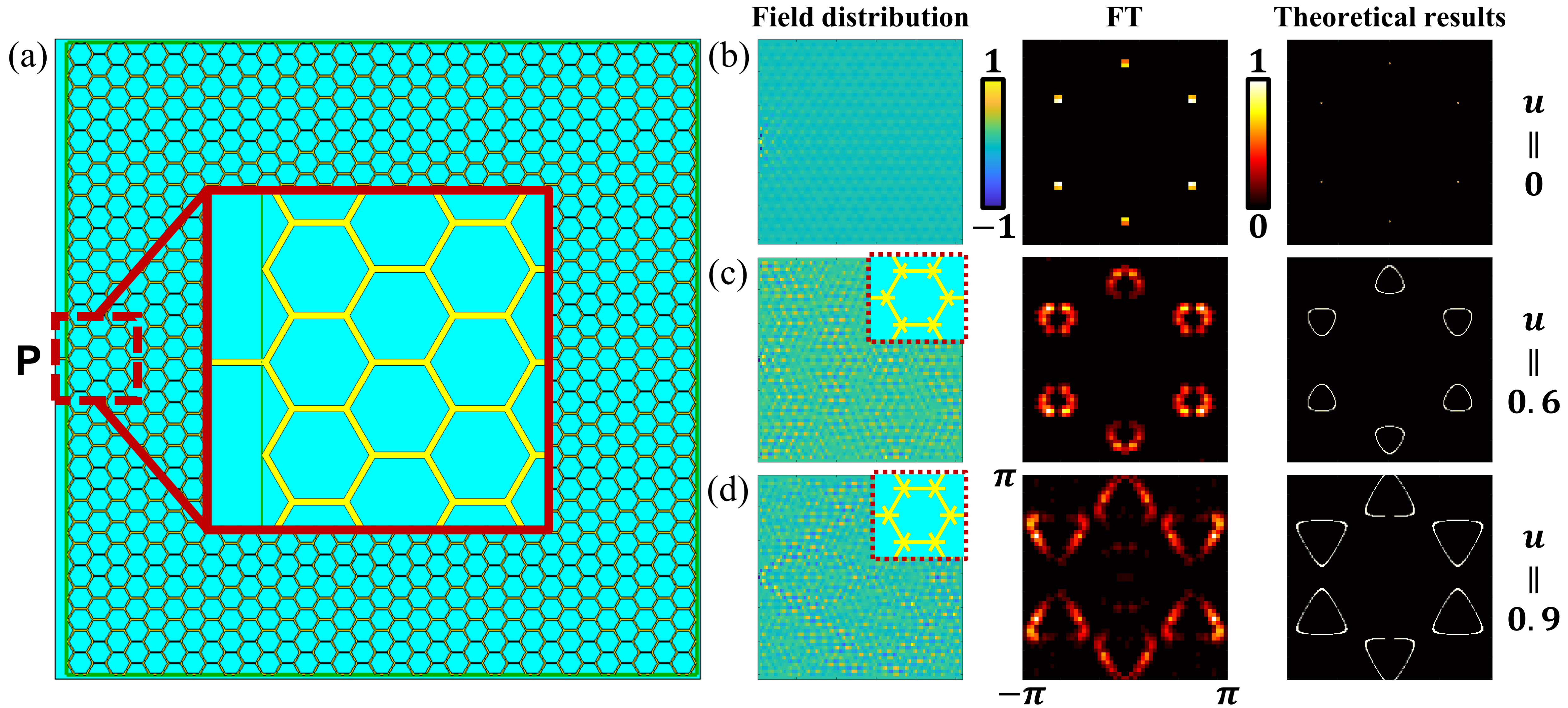
Because of the equivalence, the circuit cell of Fig. 16a can be replaced by ML as shown in Fig. 16b. Such connection creates additional regions as the red triangles in Fig. 16b, which introduce additional electrical lengths. Figure 16c is the equivalent circuit of a triangle, and the element parameters can be exactly calculated. However, for simplicity, we can take the influence into account from the view of wave propagation, for which the commercial simulator CST studio is used. When transmitting along a length of ML with parameters above, the electromagnetic wave acquires a phase shift of . Furthermore, the phase shift from one side of the triangle to another is . Therefore, we can adjust the length to 16.2 mm to decrease the electrical length. Then in Fig. 16b, the wave also acquires a phase shift of from site to . We construct the ML graphene lattice in CST (Fig. 17a) and simulate the filed distribution. A waveguide port is set at P and the field within the green box is simulated at GHz. All boundaries are set as perfect electric conductors.
After Fourier Transform (FT), the energy band section at certain momentum is achieved (Fig. 17b). The theoretical result calculated from Eq. 51 is alos given for comparison. As an upgrade of TTCs, the ML lattice also exhibits the property of momentum resolution. Moreover, there are more than one way to adjust the momentum at which the band section is obtained after FT. For example, according to the equivalence, the self-admittance terms can be easily tuned by altering the operating frequency . When , the corresponding wave number , and so does the electrical length. Thus, the self-admittance of any sublattice site, namely, the onsite potential is no longer . In addition to the way of altering , can also be adjusted at fixed by attaching a length of open or short circuit ML to sublattice sites. As shown in Fig. 16d, a length of open (short) circuit ML is equivalent to a grounded capacitor (inductor), whose admittance is
| (54) |
Therefore, attaching a length of ML to a site simply alters the self-admittance of it, adjusting the onsite potential . To demonstrate that, simulation at different onsite potentials is caused (Fig. 17c and 17d).
F.2 ML Haldane model
To make graphene topological, imaginary second-nearest neighbor hopping related with direction is added to break the time-reversal symmetry, which is the Haldane model. For ML lattice, such hopping can be introduced through a circulator (Fig. 18a). The propagation of wave in a circulator depends on the location of the three ports. For an ideal circulator, the S matrix is
| (55) |
and the corresponding admittance matrix is
| (56) |
However, an actual circulator always carries a phase shift of and the corresponding S and admittance matrices are
| (57) |
Moreover, connecting circulators to the lattice sites of ML graphene lattice also requires certain lengths of ML. To calculate the overall admittance introduced by an actual circulator, the schematic is shown as Fig. 18b. and are the current and voltage respectively, and is the length of the connecting ML. The corresponding admittance and can be calculated as Eq. 53. Denoting and the same for , , and , then
| (58) |
| (59) |
Noting that ,
| (60) |
and Eq. 59 can be transformed into
| (61) |
Substituting Eq. 61 into Eq. 60,
| (62) |
namely
| (63) |
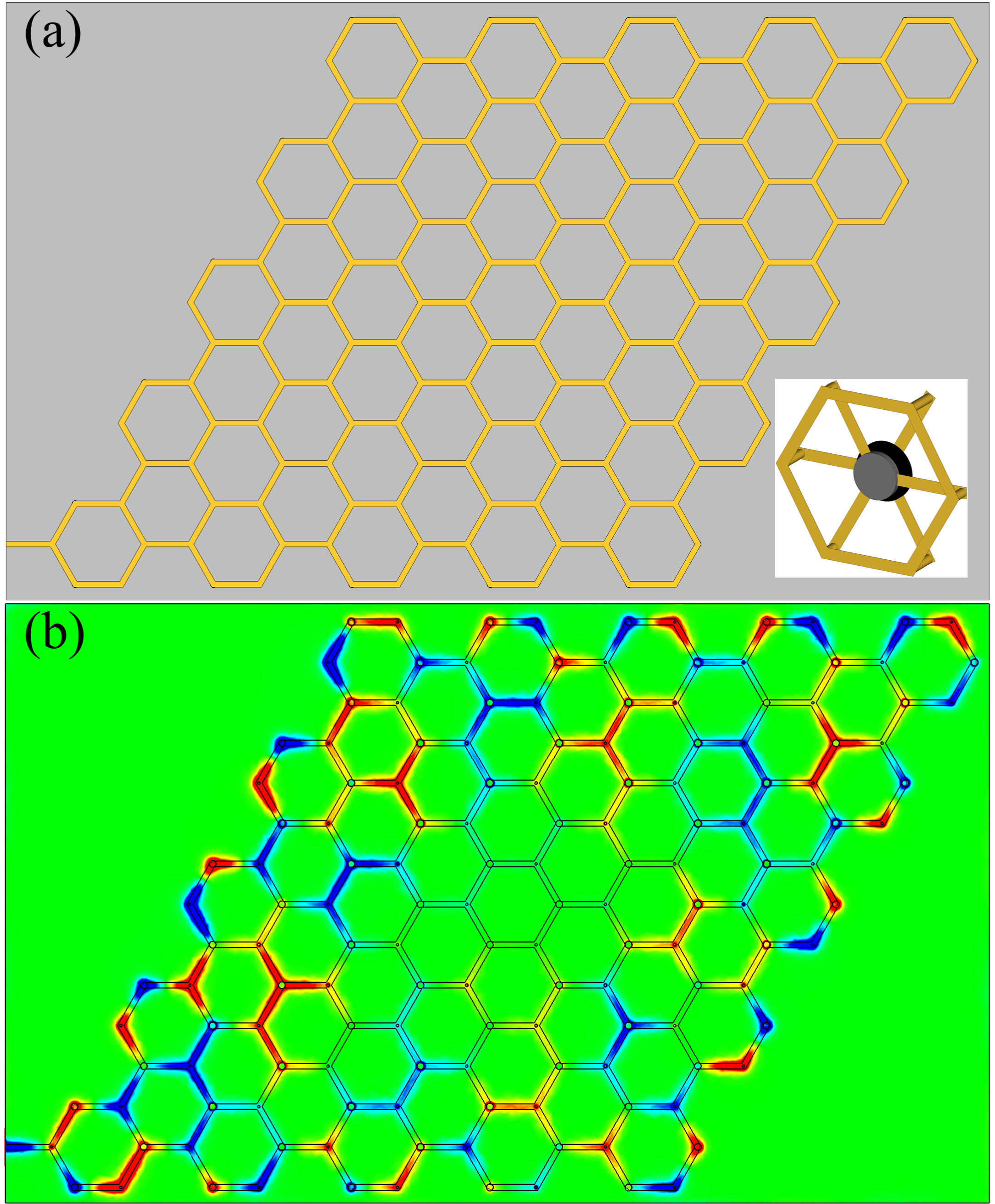
Introducing the imaginary second-nearest neighbor hopping to the ML graphene lattice with circulators, the Haldane ML lattice with armchair boundaries is constructed as shown in Fig. 19a. The Haldane ML lattice consists of 3 layers. Top layer is the ML graphene lattice with sublattice and being connected to circulators at the other 2 layers through vias. The middle and bottom layers are stirp line and ML circulators, respectively (the inset of Fig. 19a). Figure 19b shows the corresponding field distribution at GHz, which demonstrates the existence of boundary state. It should be noted that, in simulations, we use microstrip circulators as Fig. 10a and construct a 3-layer model for clarity. While for experimental realization, circulators as Fig. 18a can be used directly to simplify the structure and construct a 2-layer setup.
Appendix G Kwant simulation
In this section, we firstly introduce the details about simulating the transport of the topological junction with Kwant. Then, in order to realize nearly equivalent scattering properties of a semi-infinite conductor with finite size, the details about imaginary absorbing potential are provided.
G.1 Topological junction
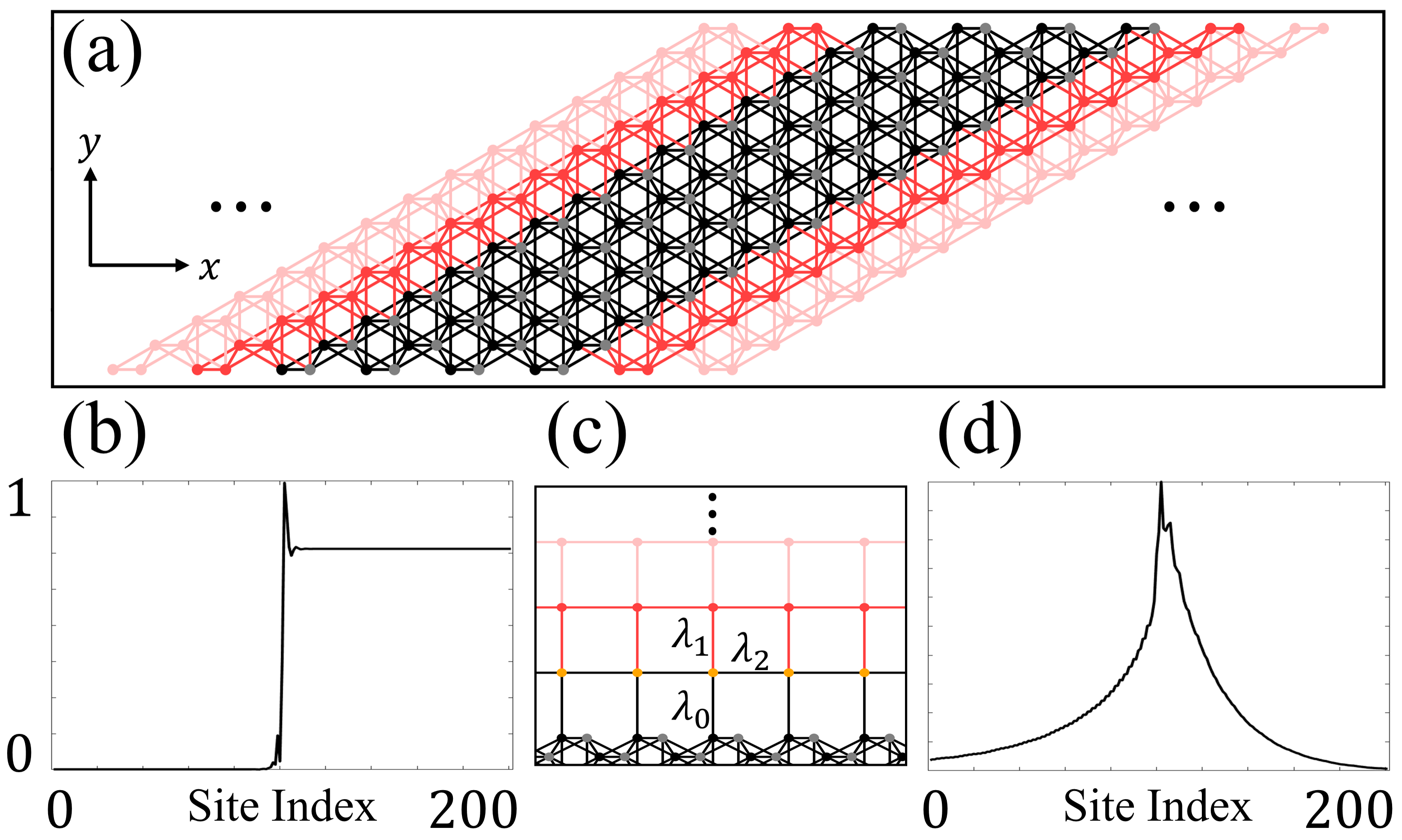
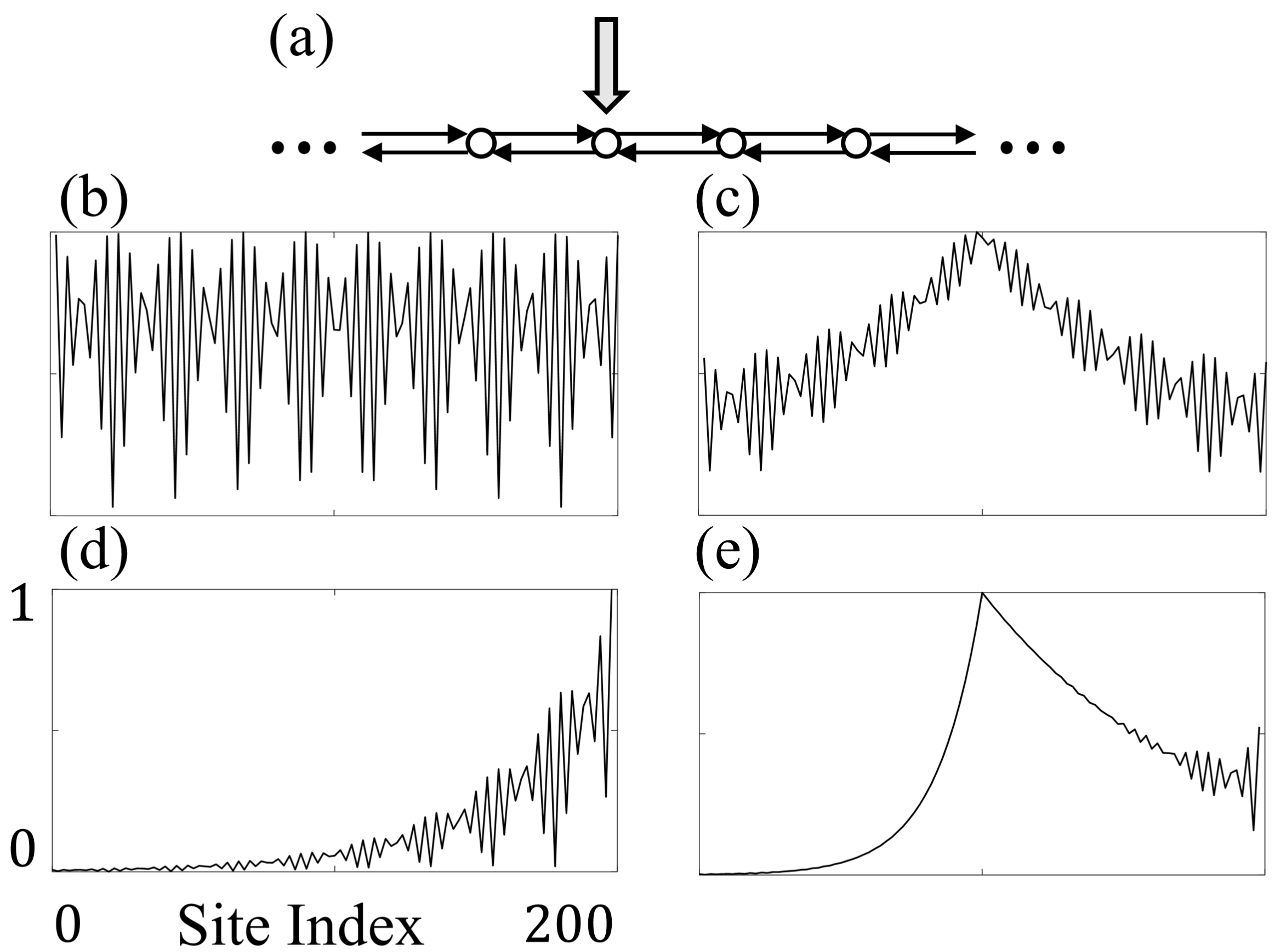
To demonstrate the non-bloch transport of topological insulator–connductor junction, Kwant, a open source Python package, is adopted. Firstly, the simulation model of a Haldane ribbon with armchair boundaries is constructed (Fig. 20a). The corresponding hoppings are set to be . Transport properties of the topological insulator are simulated by calculating the Green’s function of the upper side for 200 lattice sites. When excited at the 101st site, the response of all sites is depicted as Fig. 20b, which represents for the chiral boundary state of Haldane model. Based on the Haldane ribbon, a semi-infinite conductor with square lattice is attached to sublattice to construct the topological insulator–connductor junction (Fig. 20c). Hopping parameters of the conductor lattice are set to be and . Transport properties of the junction are simulated in the same way and at the same region as above. The corresponding response is shown as Fig. 20d. In Fig. 20b, waves cannot propagate along to the left because of the boundary state being clockwise. However, in Fig. 20d, waves decay exponentially at different rates in different directions, which represents for the non-bloch transport and can be attributed to the non-Hermiticity introduced by the Hermitian semi-infinite conductor.
G.2 Imaginary absorbing potential
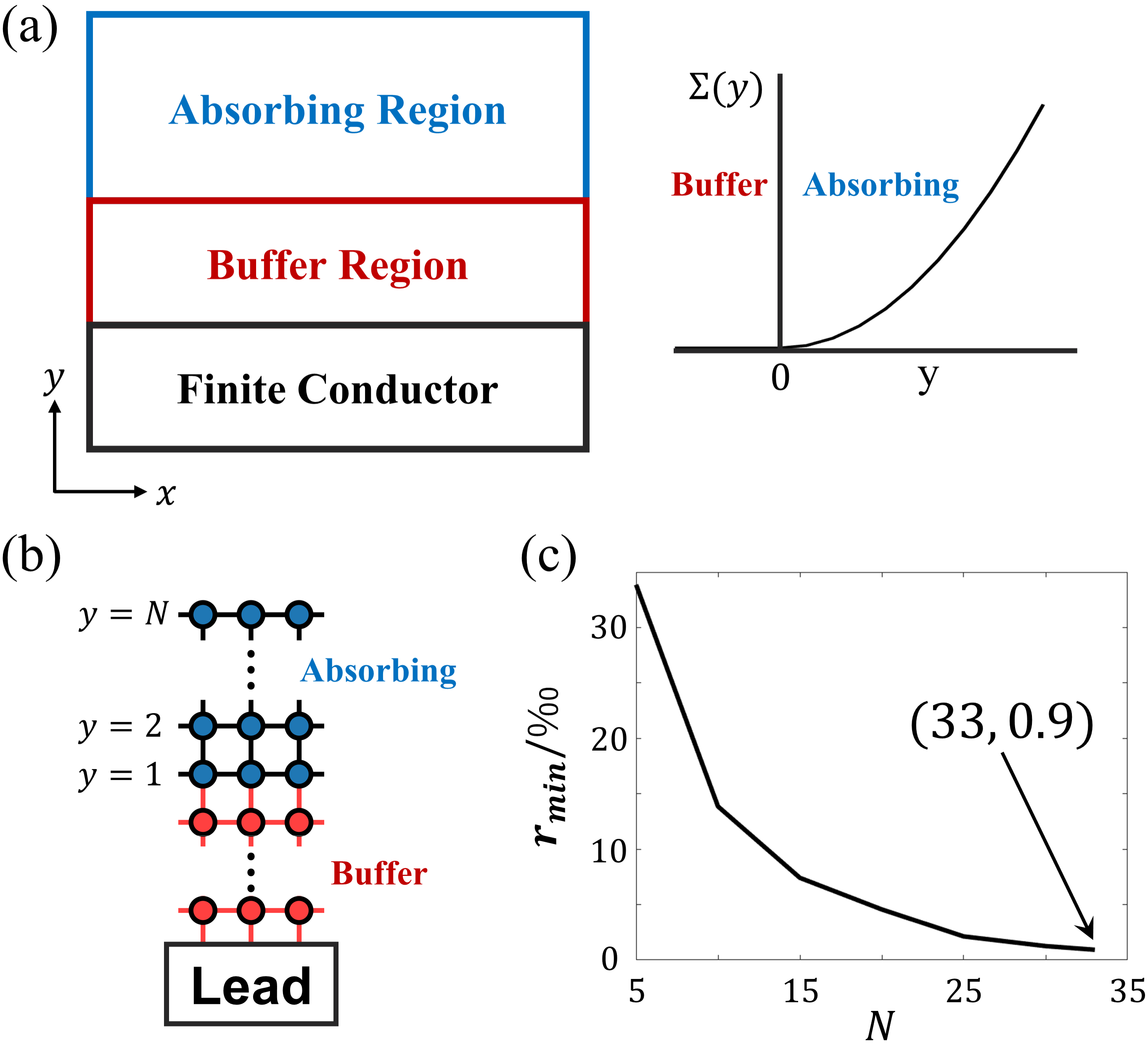
Constructing the topological junction needs for a semi-infinite conductor that is impractical for experimental setup. Therefore, imaginary potential method [52, 53] is adopted on a finite conductor to realize equivalent effects as a semi-infinite one. As shown in Fig. 21a, the method consists of two additional regions. In absorbing region, imaginary onsite potential is introduced to the lattice sites to absorb the waves propagating towards the end. Moreover, a buffer region is used to extend the propagation time of the ineluctable backscattering wave so that it would not influence the transportation of the topoligical junction in certain simulation time. According to Ref. [52], a polynomial form of imaginary onsite potential is adopted:
| (64) |
where and are controlling parameters, and is the order number counted from the start point of the absorbing region (Fig. 21b). Generally, the values of imaginary potential should be large enough so that the waves can be absorbed within a region as small as possible. However, sharp change of the values from one point to the next causes backscattering that weakens the absorption. Thus, the actual problem is the optimization about controlling parameters , , and the length of the buffer and absorbing region in . To obtain appropriate parameters, a finite square lattice with imaginary onsite potential according to Eq. 64 is constructed in Kwant (Fig. 21b). The number of sites in is 150 and the length of the buffer region in is 20. A lead is attached to the lattice to simulate the reflection. At a fixed length of the absorbing region, parameter sweep of and is performed to minimize the reflection. The same process is executed for different values of , and the variation of minimum reflectivity with is depicted in Fig. 21c. intuitively decreases with the increase of , and when , . Thus, we choose the length of the absorbing region to be 33, and the corresponding controlling parameters for are and .