††thanks: These authors contributed equally.††thanks: These authors contributed equally.
Orbital magnetoelectric coupling of three dimensional Chern insulators
Xin Lu
School of Physical Science and Technology, ShanghaiTech University, Shanghai 201210, China
Renwen Jiang
School of Physical Science and Technology, ShanghaiTech University, Shanghai 201210, China
Jianpeng Liu
liujp@shanghaitech.edu.cnSchool of Physical Science and Technology, ShanghaiTech University, Shanghai 201210, China
ShanghaiTech Laboratory for Topological Physics, ShanghaiTech University, Shanghai 201210, China
Liaoning Academy of Materials, Shenyang 110167, China
Abstract
Orbital magnetoelectric effect is closely related to the band topology of bulk crystalline insulators. Typical examples include the half quantized Chern-Simons orbital magnetoelectric coupling in three dimensional (3D) axion insulators and topological insulators, which are the hallmarks of their nontrivial bulk band topology. While the Chern-Simons coupling is well defined only for insulators with zero Chern number, the orbital magnetoelectric effects in 3D Chern insulators with nonzero (layer) Chern numbers are still open questions. In this work, we propose a never-mentioned quantization rule for the layer-resolved orbital magnetoelectric response in 3D Chern insulators, the gradient of which is exactly quantized in unit of . By theoretical analysis and numerical simulations, we demonstrate that the quantized orbital magnetoelectric response remains robust for various types of interlayer hoppings and stackings, even against disorder and lack of symmetries. We argue that the robustness has a topological origin and protected by layer Chern number. It is thus promising to observe the proposed quantized orbital magnetoelectric response in a slab of 3D Chern insulator thanks to recent experimental developments.
Band insulators can be classified into different topological phases according to different topological invariants [1, 2, 3, 4]. One important and basic topological invariant is the Chern number for two dimensional (2D) systems [2, 5, 1], which describes the winding number of hybrid Wannier centers of Bloch energy bands within 2D Brillouin zone [6], or the effective number of gapless chiral edge states [7, 6]. Those time-reversal-broken band insulators with nonzero Chern number are called Chern insulators, or quantum anomalous Hall (QAH) insulators, since they would exhibit quantum Hall effect in the absence of macroscopic magnetic field [8, 9, 10]. One can generalize the notion of 2D Chern insulators to its 3D counterpart by stacking an infinite number of 2D Chern insulators along the vertical axis [11, 12, 13, 14]. In principle, one can stack 2D Chern insulators along any direction so that one can define three independent Chern numbers , called Chern vector [15, 16], to characterize 3D band insulators. If the interlayer hopping is weak enough such that the bulk gap remains opened, such a 3D band insulator, named 3D Chern insulator, is adiabatically connected to an infinite number of decoupled 2D Chern-insulator layers.
Topological 3D band insulators are known to exhibit non-trivial orbital magnetoelectric (OME) responses. The OME coupling is defined as the change in bulk electric polarization while applying magnetic field , or equivalently the variation of bulk orbital magnetization induced by external electric field : with . This response is odd under inversion and time-reversal symmetry so that it vanishes if either of two symmetries is present. 3D time-reversal-protected topological insulators are classified by invariant [4, 17, 18, 19], which exhibits a half quantized bulk diagonal Chern-Simons OME response , modulo an integer multiple of , once the surface state is gapped out [20, 21].
However, the Chern-Simons coupling is well defined only for bulk band insulators with zero Chern number within any 2D plane in momentum space, namely with vanishing Chern vector. This is because the expression of the Chern-Simons OME coupling coefficient involves an integration of Chern-Simons 3-form defined by the occupied Bloch states over the 3D Brillouin zone [21, 20], which requires the existence of a smooth and periodic gauge throughout the 3D Brillouin zone [22, 23, 24]. However, such a gauge is non-existing for 3D Chern insulators due to topological obstruction.
Nevertheless, nothing forbids 3D Chern insulators to have a topological OME response.
Intuitively, let us consider a 3D Chern insulator with Chern vector , where with interlayer distance . What would happen if a non-disruptive electric field is applied assuming the interlayer coupling is weak? On the one hand, since 3D Chern insulator is adiabatically connected to trivial stacking of 2D Chern insulators, the off-diagonal or similar components should behave similarly as in the 2D case [25]. If a uniform electric field is applied along the axis, a transverse anomalous Hall current flowing along the direction would be induced due to the non-zero Chern number, with . The bulk anomalous Hall current would naturally generate orbital magnetization via , giving rise to an off-diagonal OME response, with its response coefficient varying linearly in real space, i.e., [25].
On the other hand, if a uniform electric field along the direction () is applied, the surface-state occupation will be different for every layer due to the vertical electrostatic potential drop.
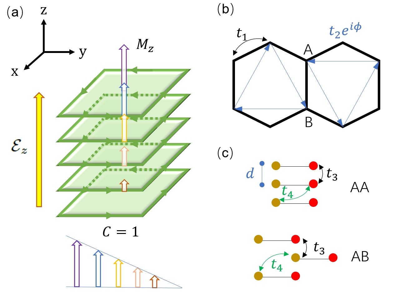
Then, the uneven distribution of electrons among the chiral edge states of each Chern-insulator layer (in the weakly coupled situation) would cause a layer-resolved , which may be manifested as a new type of diagonal OME effect which is unique to 3D Chern insulators, as schematically shown in Fig. 1(a).
Figure 1: (a) Sketch map for quasi-3D Chern insulator. When is applied, different layers have layer-dependent responses that the layer-resolved s change linearly. (b) Honeycomb lattice for 2D Haldane model on which the hopping and are marked. (c) Two ways of stacking: AA-stacking and AB-stacking. Unless mentioned ad hoc, we always use , , , , and the staggered mass term is set to zero.
Layer-resolved orbital magnetization–
Although the total diagonal , only relevant in 3D case, is vanishing if a mirror plane exists,
the layer-resolved (with layer index ), which measures the change of layer-resolved orbital magnetization under a weak , may be finite. To define in the thermodynamic limit, we need to define a layer-projected orbital magnetization using [26]
(1)
where and are the projection operators onto the occupied and unoccupied subspaces, respectively. The chemical potential is at charge neutrality, are 2D position operators and is the system area in the - plane. “Tr” in the above equation means taking the trace over the whole Hilbert space.
Since would break the translation symmetry in the direction, it is natural to consider a slab geometry so that can be suitably expressed in the basis of the Bloch function [27]
(2)
where means sublattice index in the unit cell, layer index, band index and number of 2D layers in the direction.
Then, we can express in the Bloch function basis as
(3)
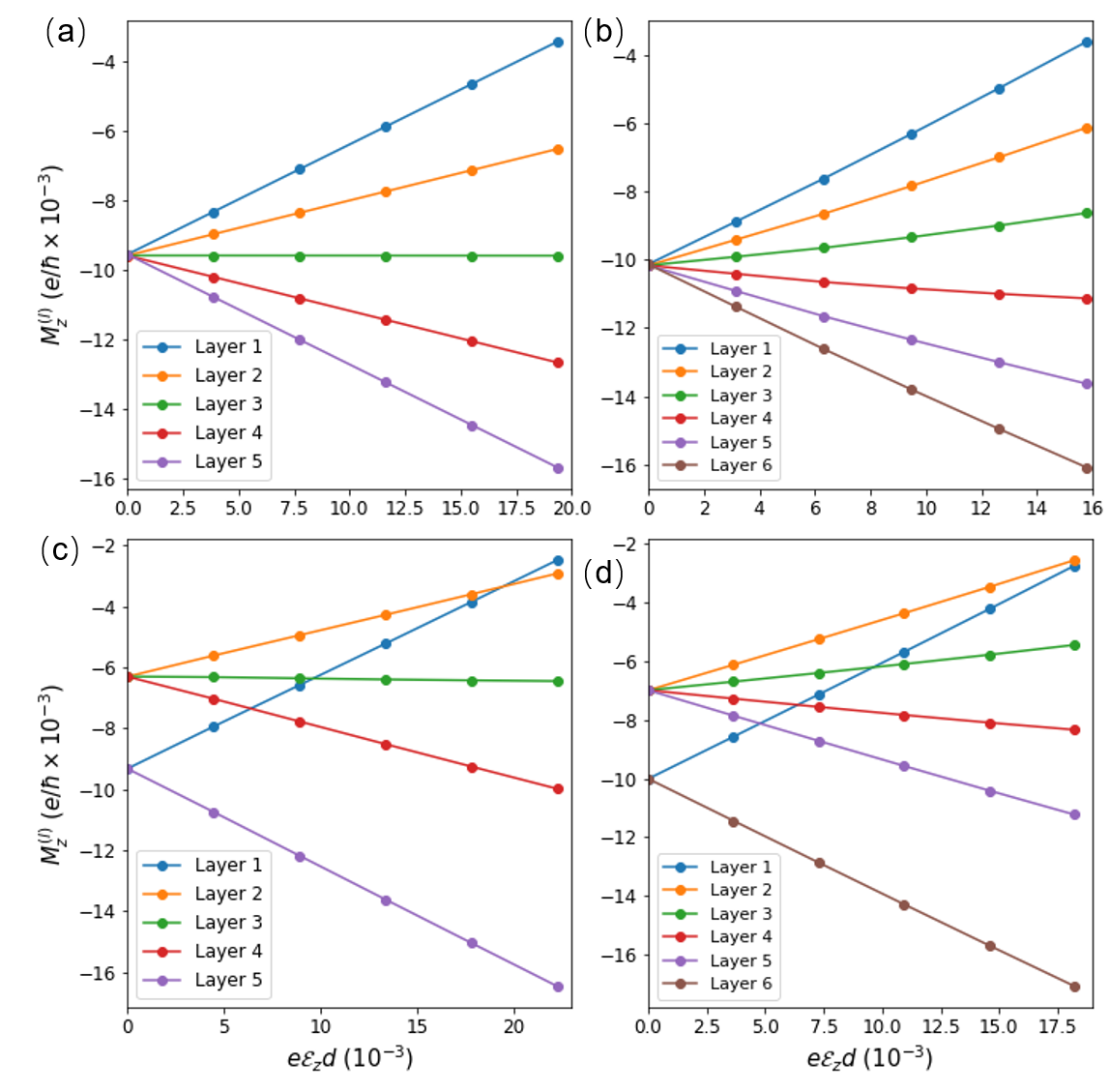
where for occupied/empty states, is the periodic part of and with is the antisymmetric tensor. The layer-resolved magnetization of the -th layer is then defined by summing over all the degrees of freedom except the layer index. For illustration, we model the 2D Chern-layer constituents of 3D Chern insulator by 2D Haldane model. Without loss of generality, the Chern number for each layer alone is set to be and interlayer coupling is weak such that the bulk gap remains finite. Details of parameters is shown in Fig. 1(b). In our numerical calculations, we consider two types of stacking, and , as illustrated in Fig. 1(c) and the slab consists of five or six layers. The k mesh is set to . The chemical potential is determined by looking for charge neutrality point in the same system with open boundary conditions. Then, can be obtained numerically by finite difference, namely the ratio between change in and finite external electric field .
We find that varies linearly for weak electric field for both types of stacking, independent of number of layers (see Fig. 1 in Supplemental Materials [25]).
The obtained is quantized to integers if odd or to half-integers if even, as shown in Table 1. The distribution is symmetric to the central plane of the system and the total is indeed vanishing as dictated by mirror symmetry. The quantization is only limited to precision due to the finite-size effect [25].
Table 1: Layer-resolved in units of obtained by numerical finite difference and those evaluated by perturbation theory given in the parenthesis.
Layer Index
1
2
3
4
5
6
AA,5
1.9893 (1.9905)
0.9971 (0.9982)
-0.0010 (9.80E-14)
-0.9990 (-0.9982)
-1.9918 (-1.9905)
AB,5
1.9289 (1.9739)
0.9525 (0.9973)
-0.0456 (5.29E-05)
-1.0424 (-0.9974)
-2.0194 (-1.9739)
AA,6
2.5365 (2.4894)
1.5444 (1.4974)
0.5464 (0.4992)
-0.4519 (-0.4992)
-1.4502 (-1.4974)
-2.4423 (-2.4894)
AB,6
2.4863 (2.4727)
1.5098 (1.4962)
0.5123 (0.4987)
-0.4855 (-0.4990)
-1.4828 (-1.4963)
-2.4592 (-2.4727)
Note that applying a vertical electric field induces a constant electrostatic potential drop between the two adjacent layers. Each layer acquires a layer-dependent on-site energy . If is so weak that the electrostatic potential drop between the top and bottom layers can be treated as a perturbation to the system, then can be determined semi-analytically using perturbation theory. We need to factorize all the changes linear in among , , and and chemical potential . Then, after considerable algebra, a semi-analytic formula including all the above four contributions for is derived. Details are given in Sec. III of Supplemental Materials [25]. We say “semi-analytic” since the determination of the chemical potential still requires solving numerically the system with open boundary condition, which is unavoidable due to the presence of gapless surface states in 3D Chern insulators.
Therefore, one can directly calculate using only the energy and Bloch functions of the unperturbed system. As shown in the parenthesis of Table 1, obtained by semi-analytic perturbation theory follow exactly the same quantization rule as those calculated by numerical finite-difference method.
Since the layer index , the choice of which is a priori arbitrary, appears in perturbation formula [25], the final formula seems to depend on the “layer index gauge choice” at the first glance. Eventually, we can prove that the layer-resolved responses turns out to be “layer index gauge independent” as proved in Sec. IVof Supplemental Materials [25].
It worth a while to think that in a slab geometry, since the more layers there are, the greater the response coefficients on both sides, would not the corresponding diverge if the total number of layers went to infinity? However, when the total number of layers increases to a certain extent, even a very small electric field applied in the direction will cause Zener tunneling and the system then is no longer an insulator. This imposes a truncation to the otherwise diverging layer-resolved OME response.
Table 2: Difference between of neighboring layers in units of obtained by numerical finite difference and those evaluated by perturbation theory given in the parenthesis.
AA,5
-0.9921(-0.9922)
-0.9982(-0.9982)
-0.9980(-0.9982)
-0.9927(-0.9922)
AB,5
-0.9794(-0.9766)
-0.9981(-0.9972)
-0.9968(-0.9972)
-0.9770(-0.9766)
AA,6
-0.9921(-0.9920)
-0.9980(-0.9982)
-0.9983(-0.9983)
-0.9983(-0.9982)
-0.9921(-0.9920)
AB,6
-0.9764(-0.9766)
-0.9976(-0.9975)
-0.9978(-0.9977)
-0.9973(-0.9972)
-0.9764(-0.9765)
To understand the origin of the quantization in , one can consider the simplest case where neighboring layers are completely decoupled from each other such that the Hamiltonian is block diagonal in layer space. The only contribution to comes from . Then, we can prove exactly that the difference in between the two neighboring layers is quantized (see Sec. V of Supplemental Materials [25])
(4)
or equivalently,
(5)
This quantization rule remains robust even in the presence of considerable interlayer hopping, as shown in Table 2 with .
Knowing that the total is vanishing, we can deduce that is integer quantized in units of for odd number of layers or half-integer quantized for even number of layers, consistent with the previous findings. This is expected since the interlayer decoupled case is adiabatically connected to the above weakly coupled case.
The topological origin of the quantization rule is more transparent if we invoke the interpretation of OME coupling by the bulk-edge correspondence.
It is precisely the chiral edge states that give rise to the quantized in a 3D Chern insulator.
Intuitively, 3D Chern insulator is formed by stacking 2D Chern insulators with, for example, . There must be chiral edge states flowing around each layer and a charge neutral crosses with all the edge states. A weak uniform induces different occupation for the edge states of different layer when the system is back to equilibrium. The redistribution of electrons among different layers can be equivalently modelled by layer-resolved chemical potential , where is the chemical potential in the absence of electric field and such that the total number of electrons is unchanged, namely . Since the chemical potential is in the bulk gap, all the changes in stems from the surface-state contribution [6, 27, 28, 29]:
(6)
Therefore, we can get a simple formula for as follows
(7)
consistent with Eq. (4) knowing that . The behavior for even and odd number of layers are given precisely by the shift . This picture is exact in the interlayer decoupled case and can be generalizable to the weakly coupled case by the topological argument, as long as the bulk gap is not closed so that the layer Chern number remains quantized [30, 31, 32, 33].
Layer-resolved electric polarization–
The same quantization rules also exist for a genuine 3D Chern insulator in which the vertical stacking of 2D Chern layers goes to infinity with periodic boundary condition. To evaluate , it is convenient to calculate the change of layer-resolved polarization [34] under a finite weak magnetic field . By adopting a magnetic field commensurate with crystalline lattice, we restore the translational symmetry in all the three directions such that is determined in the thermodynamic limit without explicitly invoking finite-size effect in the slab geometry.
Before calculating , we need to properly define the electronic contribution of layer polarization , which can be written in terms of the maximally localized Wannier center for each layer in the stacking direction, denoted as [34]
(8)
where is the size of the 2D magnetic unit cell, interlayer distance is constant and the averaged maximally localized Wannier center is proportional to the averaged Berry phase calculated by parallel-transport method [34, 35]
(9)
where is the total number of k points in the - plane. In practice, parallel-transport method gives Berry phases, which are then categorized into of different layers based on the smallest distance criterion. Here is the number of layers in an artificially chosen slab, and here we consider infinite stacking of slabs with periodic boundary condition imposed, so that the vertical size of 3D Brillouin zone is set to .
Using the same parameters as before, it turns out that even with a relative strong interlayer coupling ( is of the same order magnitude as ), the Wannier centers sit closely to each layer [25]. In practice, we use a magnetic field such that the magnetic flux piercing the atomic unit cell is . A k mesh is adopted for numerical calculations. We obtain a similar quantization rule for as shown in Table 3. Compared with previous calculations, the quantization is way better () in such situation with fully periodic boundary condition.
Table 3: Layer-resolved response in units of [] in the thermodynamic limit using .
Layer Index
1
2
3
4
5
AA,4
1.499985
0.50002
-0.49998
-1.50002
AA,5
1.999985
1.00002
0.00002
-1.00000
-2.00001
AB,4
1.50401
0.49599
-0.50555
-1.49445
By Streda formula [36], when a finite magnetic field is turned on, states would flow between valence and conduction bands while keeping the chemical potential in the bulk gap. The number of transferred states is proportional to the Chern number of the system. For example, for = 4, when is switched on, four states would flow from conduction to valence bands as dictated by four 2D Chern layers. Most saliently, we observe that these four states are tied exactly to four equidistant Wannier centers from the four coupled 2D Chern layers, respectively. Indeed, the quantization rule remains robust as long as the extra -induced flowing states are evenly distributed among the equidistant Wannier centers, which do not necessarily coincide with the layer position. The validity of Eq. (4) even do not require uniform layer charge density when . The only requirement is that the bulk gap remains opened and layer Chern number remains exactly quantized as interlayer coupling is turned on, which is obvious for disorder-free 3D Chern insulators where is a good quantum number.
Following the above argument, here we give a more rigorous proof of the quantization rule Eq. (4) for interlayer-coupled 3D Chern insulators. Under finite , due to Streda formula, the layer charge density follows for all layers, with denoting layer Chern number. Therefore, whenever there is a change in the total charge density induced by , it has to be equally distributed to each layer as long as is still well defined and quantized. The additional layer charge density leads to a change in layer-resolved polarization , which is induced by . Thus, the layer-resolved OME coupling is given by:
(10)
Note that does not necessarily sit at the corresponding layer position due to lack of symmetry. Let as in our cases with constant interlayer distance , then Eq. (4) follows immediately. For illustration, let us consider a slab breaking inversion and mirror symmetry by introducing a different on-site energy only on the first layer (denoted as substrate layer) such that the total response is finite.
In practice, the slab consists of five -stacked layers. We set the on-site energy of the first layer to be varying the amplitude of . We calculate using Eq. (3) with mesh. As shown in Table 4, although itself does not follow any quantization rule [25], the difference between the neighboring layer-resolved responses is quantized to layer Chern number as predicted. This shows that the most intrinsic quantization rule is Eq. (4). Nevertheless, symmetry can impose additional constraints on the values of . For example, mirror or inversion symmetry forces to be integer or half integer, as observed in Table 1 and 3.
Table 4: Difference between neighboring layer-resolved response in units of [] in systems with substrate.
-0.9972
-0.9972
-0.9972
-0.9972
-0.9972
-0.9972
-0.9972
-0.9972
-0.9972
-0.9972
-0.9972
-0.9972
-0.9934
-0.9978
-0.9978
-0.9937
-0.9840
-0.9996
-0.9990
-0.9849
Therefore, we see from above that the quantization rule Eq. 4 is precisely given by the integer number of transferred states projected to each layer, which essentially originate from the quantized layer Chern number and topological edge states in open boundary condition. This reveals again the topological nature of the quantization in .
Robustness of quantization–
In the presence of disorder, as long as the bulk gap is not closed by disorder such that layer Chern number remains well defined and quantized, the change of layer charge density induced by magnetic field would still remain quantized as dictated by Streda formula. Thus, the quantization rule of Eq. (4) is still valid. More numerical evidence of the robustness of Eq. (4) in the presence of disorder is given in Table 5.
In practice, we need to calculate numerically by finite-difference in the fully open boundary conditions. Disorder is modelled by random on-site potential. Two types of disorder are introduced. The first type is that on-site energy only fluctuates in-plane repeating itself among all the layers. The second type breaks the translation symmetry such that on-site energy fluctuates among all the sites of all layers. We consider 15 disorder configurations and then analyze the results statistically. Here we set , , and a strong disorder with amplitude .
Table 5: Statistical layer-resolved response in units of [] in the presence of disorder using (fluctuation std()).
layer index
2
1
0
-1
-2
bare
1.9401
0.9934
-0.0034
-0.9875
-1.9426
Type-I average
1.9398
0.9932
-0.0034
-0.9874
-1.9422
Type-II average
1.8965
1.0213
0.0512
-0.9527
-2.0127
Type-I fluctuation
2.73E-04
1.47E-04
1.34E-05
1.37E-04
2.82E-04
Type-II fluctuation
0.0443
0.0584
0.0600
0.0286
0.0407
As shown in Table 5, the quantization rule remains good statistically not only for Type-I disorder preserving layer translation symmetry but also Type-II disorder breaking it. This is because the amplitude of the disorder does not close the gap so that layer Chern number can still be well defined.
Discussions–
Two subtleties worth mentioning in the thermodynamic limit that is only defined modulo and only the difference in is physically measurable. Both observations are rooted in the indeterminacy of electric polarization that the choice of unit cell is arbitrary. Here is the number of inequivalent layers within the smallest unit cell. Nevertheless, the difference between of two neighboring layers is measurable and is a topological quantity. The ambiguity in the branch choice of is either fixed by the symmetry constraint on the total bulk response or by boundary condition at the surface.
In summary, we propose a diagonal layer-resolved OME response in 3D Chern insulator, which have not been studied before. Most saliently, this OME response is quantized or half-quantized to in the presence of inversion or mirror symmetry. Furthermore, even lack of symmetries, the gradient of this OME coupling is still exactly quantized in unit of given by Eq. (5). We demonstrate the robustness of the quantization rule against disorder through numerical calculations and topological argument using the Streda formula. Such considerable and quantized difference between layer-resolved OME is in principle measurable in experiments. For example, in a slab system, applying an out-of-plane electric field would induce a quantized change in orbital magnetization at the top and bottom layers, which may be probed by SQUID-on-tip microscope [37, 38].
Acknowledgements.
This work is supported by the the National Natural Science Foundation of China (Grant No. 12174257), National Key R & D Program of China (Grant No. 2020YFA0309601).
Vanderbilt [2018]D. Vanderbilt, Berry phases in
electronic structure theory: electric polarization, orbital magnetization and
topological insulators (Cambridge University
Press, 2018).
Bernevig and Hughes [2013]B. A. Bernevig and T. L. Hughes, Topological Insulators
and Topological Superconductors (Princeton
University Press, 2013).
Chang et al. [2013]C.-Z. Chang, J. Zhang,
X. Feng, J. Shen, Z. Zhang, M. Guo, K. Li, Y. Ou, P. Wei, L.-L. Wang, Z.-Q. Ji, Y. Feng, S. Ji, X. Chen, J. Jia, X. Dai, Z. Fang, S.-C. Zhang, K. He, Y. Wang, L. Lu, X.-C. Ma, and Q.-K. Xue, Science 340, 167 (2013), https://www.science.org/doi/pdf/10.1126/science.1234414 .
[25]See Supplemental Materials for: (a)
Definition of layer-resolved orbital magnetization and layer Chern number;
(b)Layer-resolved orbital magnetization varies linearly with electric field;
(c) Derivation of perturbation theory for layer-resolved orbital
magnetoelectric response; (d) Proof of layer index gauge Invariance in the
formula of perturbation theory; (e) Proof of the quantization of
layer-resolved orbital magnetoelectric response in the absence of interlayer
coupling; (f) More details on numerical evaluations and discussion on
finite-size effect.
Zhou et al. [2023a]H. Zhou, N. Auerbach,
M. Uzan, Y. Zhou, N. Banu, W. Zhi, M. E. Huber,
K. Watanabe, T. Taniguchi, Y. Myasoedov, et al., Nature 624, 275 (2023a).
Supplemental Materials of “Orbital magnetoelectric coupling of 3D Chern Insulator”
I I. Expressions of layer-resolved orbital magnetization and layer Chern number
Our definition of layer-resolved orbital magnetization is inspired from the existing definition of local orbital magnetization given by [26, 27]. In this section, we will derive several expressions for layer-resolved orbital magnetization in a slab. We also define layer Chern number using local Chern marker at the end of this section.
I.1 Naive definition of layer-resolved orbital magnetization
From classical electrodynamics, the orbital magnetization of a macroscopically homogeneous system is given by
(1)
where is the volume of the system, r is the position and j is the current density. Note that the magnetic moment m is extensive while the magnetization M is intensive. In the thermodynamic limit with periodic boundary condition (PBC), a quantum expression for orbital M in 2D case, namely , can be written as
(2)
where is the system’s Hamiltonian, is the total area, is the elementary charge, and s are the eigenstates. Here, only spinless case is discussed. The first equality comes from . The last equality use the occupied-state projector . In the following, we also need the empty-state , the complement of . So, we give their definition together
(3)
The trace operation is to sum over all the eigenstates of the Hilbert space.
Note that this expression only applies to systems with open boundary condition (OBC). This is because position operators are ill-defined in the thermodynamic limit and terms like diverge. This formula is particularly useful when we introduce disorder in the system in OBC. It contains both the contribution of circulation of the current density from the bulk and the contribution from the surface. Then, one can define layer-resolved orbital magnetization as
(4)
where the atomic lattice basis represents the site at layer , sublattice of unit-cell R.
I.2 Definition of layer-resolved orbital magnetization in the thermodynamic limit
In the thermodynamic limit namely with PBC, we can derive another expression for [26] starting from Eq. (2). Since
(5)
then
(6)
where
(7)
Here we use the fact that , since
(8)
Finally, we get
(9)
or more generally,
(10)
where the summation over repeated indices is implied and is the anti-symmetric tensor with .
The key observation is that and are well-defined and regular even in an unbounded system within PBC. In principle, Eq. (9) only applies to a system which remains gapped both in bulk and at edges (since we assume ), and therefore does not apply, as such, to Chern insulators. However, we can make the substitution of for Chern insulators or metals [26]. Under this substitution, Eq. (9) is suitable to both systems with PBC and those with OBC.
We try to get the k-space expression [27] of Eq. (9) in a slab with PBC in the plane but finite in the direction, namely Eq. (3) in the main text. Suppose the eigenstates of the slab are . First, we need to evaluate
(11)
where the third equality comes from .
Here we choose to normalize the eigenstates over the unit cell , so , while the definition of projectors is normalized to unity (). Therefore, we can express the projectors as
(12)
Similarly,
(13)
Then,
(14)
where and . The second equality comes from and since .
With anti-symmetric tensor, it is convenient to write
(15)
where the second term in the parenthesis is vanishing by because of interchangeable indices. So,
(16)
Similarly,
(17)
Suppose the slab consists of layers in the direction. The Bloch function can be written as
(18)
where the Fourier basis is defined as
(19)
where means sublattice and is layer index. The corresponding normalization relation becomes
where the layer-resolved orbital magnetization of the -th layer is defined by summing all the degrees of freedom except layer . As discussed before, when considering Chern insulators having surface contribution, one needs to replace and in the previous formula. Then, Eq. (3) of the main text is then derived.
I.3 Layer Chern number
In the same spirit, we can also define layer Chern number for a slab using local Chern marker [27, 33]
(24)
In the Fourier basis, we can write down the k-space expression for layer Chern number
(25)
II II.Layer-resolved orbital magnetization under finite vertical electric field
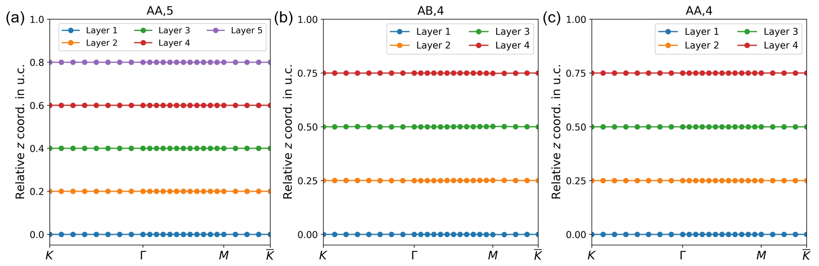
Figure 1: Layer-resolved of the slab under several for different stacking ways and total layer numbers: (a) AA stacking, 5 layers; (b) AA stacking, 6 layers; (c) AB stacking, 5 layers; (d) AB stacking, 6 layers.
In this section, we present the numerical results that varies linearly with weak electric field for both types of stacking, independent of number of layers, as clearly shown in Fig. 1. Here, we calculate using the definition Eq. (23).
III III.Perturbation theory for layer-resolved orbital magnetoelectric response
When a vertical electric field is applied to a slab, our perturbed Hamiltonian reads: . Suppose the electric field is so weak such that bulk gap is not closed and the potential drop between the top and bottom layer is the smallest energy scale in the system. The idea is to express Eq. (23) of perturbed Hamiltonian using the information of . By singling out the terms proportional to , the layer-resolved orbital magnetoelectric response is then derived by .
Let us first focus on the first-order correction in to all terms in Eq. (23). First, the correction in wavefunction reads
(26)
where the upper index “” means the quantity defined for non-perturbed Hamiltonian . The third line comes from , in which is the layer index and is the interlayer distance.
The correction in the Fourier expansion reads
(27)
The derivatives of the wavefunction reads
(28)
with Berry connection . Note from Eq. (23) that we only need to calculate with so we can omit the first term in Eq. (28). We also note that with . Therefore we need to single out the first-order correction to by expanding all other terms. The simplest one would be
(29)
Let’s now expand the second term in Eq. (28). Since
so,
Finally,
(30)
where .
With all the ingredients derived above, we can expand Eq. (23) to the first-order of field. Typically, we need to treat terms like:
Then
(31)
Now we need to explicit , and . First,
(32)
where .
(33)
(34)
Now we further:
(35)
where .
For simplicity, we introduce the following shorthand notations:
(36)
Then, for example, the expressions involving velocity operators can be rewritten as
So, we decompose Eq. (31) into four contributions: to .
We now explicit the first-order correction in : Eq.(39) and Eq.(40)
(43)
Then, the first-order correction in becomes
Now, we are ready for Eq. (23) of the perturbed system. The first part reads
the second part reads:
To the first-order in , we only need to consider terms related to , and .
Until now, the correction of the chemical potential has not been considered yet, which can be written as when field is applied. Unfortunately, the correction in cannot be expressed solely by the information extracted from with PBC. This difficulty is deeply inherited from the definition of chemical potential in the grand canonical ensemble, which requires a boundary between the system and the exterior bath. For trivial band insulator, the correction in chemical potential is unimportant as long as it is still in the gap. However, for Chern insulators having conducting edge states (as in our case), the correction in chemical potential should be seriously taken into account. This reflects the importance of edge states while evaluating measurable quantities in topological insulators.
Let us first look what to change if considering the correction in . First, only substitutions should be made in and because the rest of terms is already of first-order. As for , we should take into consideration. Our solution to is to use an auxillary system with OBC, conjugate to the system with PBC. Here, we mean “conjugate” by that both systems have the same level of discretization, in other words the back and forth Fourier transformation is normalized to unity. For example, if we consider a system with PBC of k mesh in the Brillouin zone, its conjugate OBC system is a superlattice of unit cells. For isolated system, a weak external electric field cannot change the particle number of system. So, if the system is half-filled, one determine by
(44)
where is the first-order correction in the energy of the highest filled state and the lowest empty state, respectively, for the conjugate system with OBC.
We can of course apply perturbed theory to the auxillary system, then can be formally written as
(45)
where is the form factor for the conjugate system. This expression singles out layer index, which would be useful in the next section. Meanwhile, we can also factorize the layer index out for
(46)
Then, the formula for is derived by singling out the electric field and breaking the sum over layer index into parts for each layer, respectively, in Eq. (23).
Note that the derivation above requires energy levels to be non-degenerate, otherwise the denominator would be vanishing. This should not worry us since the energy bands are non-degenerate except at some high-symmetry points if interlayer coupling is turned on. We observe that the energy bands are all non-degenerate for AA stacking and degenerate at for AB stacking. The degeneracy at is protected by space symmetry of the slab. In principle, we can choose a gauge such that the Hamiltonian is block diagonal at this degenerate point then separately apply non-degenerate perturbation theory as above. In practice, we omit the contribution from the degeneracy point which would affect too much the accuracy as long as the mesh is sufficiently fine.
IV IV.Proof of layer index gauge invariance
We see from above that layer index appears explicitly in the expressions from to . It seems that the results would depend on the gauge choice of layer index, which is a priori arbitrary. For example, if there are five layers, we can name them as or or in other similar ways. In this section, we will prove that the results of are independent of the gauge choice of layer index. Without loss of generality, this is equivalent to prove that the expression of , and is vanishing if setting . Let us see what these terms become. For , we have
(47)
As for ,
(48)
thus, . And
(49)
So, the gauge invariance of layer index for is proved.
V V. Proof of the quantization rule in the interlayer decoupled case
In this section, we will prove rigorously the quantization rule Eq. (4) in the main text for the interlayer decoupled case. Then, the total Hamiltonian is obviously block-diagonal in the layer space. Each diagonal block is the Hamiltonian of every monolayer and they are all the same. If we diagonalize the full Hamiltonian, there are exactly degenerate energy valence bands and degenerate energy conduction bands if the slab consists of layers. Without loss of generality, we can associate valence band with layer index , respectively. Similarly, we can also do the same for the conduction band with layer index , respectively. This leads to
(50)
for the band is the valence/conduction band, respectively.
Thus,
(51)
Meanwhile,
Thus,
(52)
If , Eq. (52) equals obviously. If , since is also block-diagonal, the expression must be zeros as well. To sum up, also contributes .
Now we turn to :
where we use a similar mapping as Eq. (50) for the system with OBC to derive the first equality. The last equality comes from the fact that is also block-diagonal. Note that this expression is precisely the Chern number of monolayer. Therefore, if there are odd layers in system, the response is integer quantized; if is even, the respectively is then quantized to half-integer. Then, the quantization rule Eq. (4) in the main text is automatically proved for the interlayer decoupled case.
VI VI. Details on numerical evaluations and finite-size effect
In this section, we provide more details on the numerical calculations including the calculations of and layer Chern number.
VI.1 Layer-resolved orbital magnetoelectric response of slab
In a slab system, we calculate using . We employ three approaches in our study. The first one is to calculate in the absence and in the presence of weak electric field using Eq. (23), then get by finite difference. In practice, we calculate for a series of weak electric field such that the response is still in the linear regime. Then, we fit the first four points to get the slope of the straight line and thus . We use this for a slab with PBC in the plane.
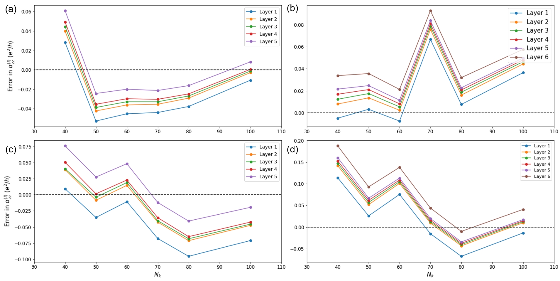
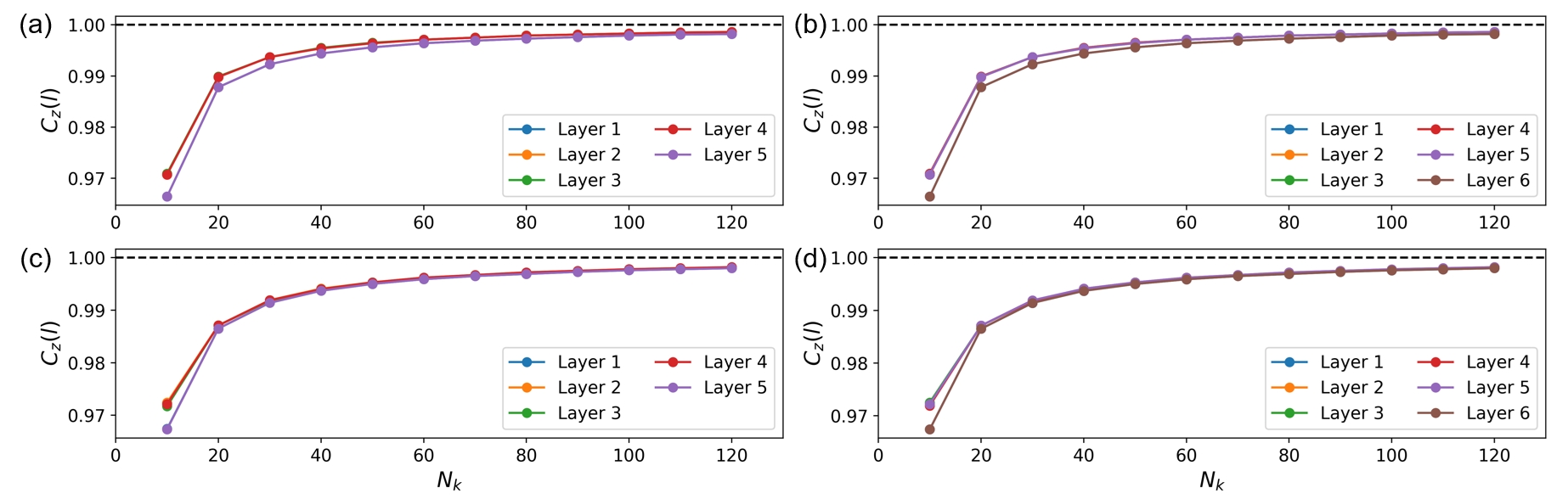
Figure 2: Error in with respect to the quantized value using finite-difference method. (a) AA stacking, five layers; (b) AA stacking, six layers; (c) AB stacking, five layers; (a) AB stacking, six layers.
In Fig. 2, we show how the quantization is improved when we refine the k mesh. We see that the improvement is not monotonic but oscillating. The main source of error comes from the determination of chemical potential given by an auxillary system with OBC. Note that this is also the method we use to evaluate in the presence of substrate. More results for those shown in the main text are given in Table 1 where k mesh is . We see that is not quantized in the presence of substrate and interlayer coupling because of inversion or mirror symmetry breaking.
Table 1: Layer-resolved response in units of [] in systems with substrate.
2.4930
1.4958
0.4986
-0.4986
-1.4958
2.1742
1.1771
0.1799
-0.8173
-1.8145
1.8602
0.8630
-0.1342
-1.1314
-2.1286
2.3786
1.3852
0.3874
-0.6104
-1.6041
1.9530
0.9690
-0.0306
-1.0296
-2.0144
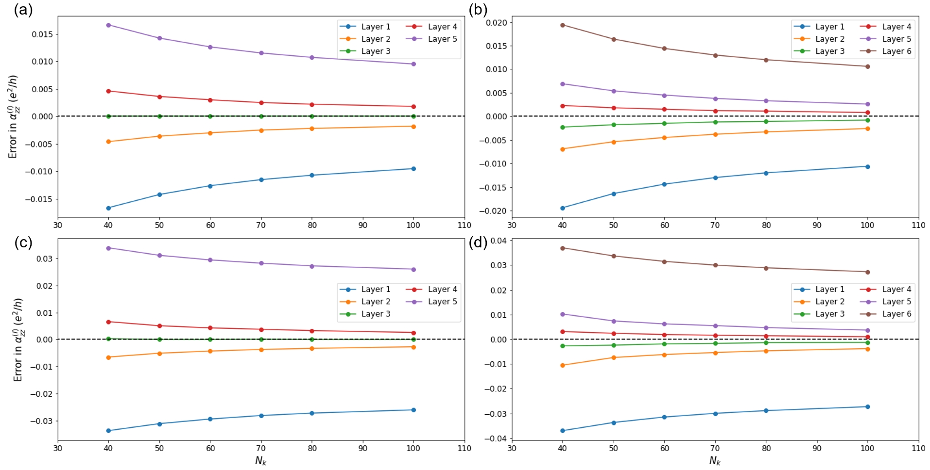
The second approach is to calculate directly applying perturbation formula given above. In Fig. 3, we show how the quantization is improved when we refine the k mesh. Compared to the first approach, one advantage of the perturbative approach is that the quantization gradually improves as the mesh becomes finer. We also note that another advantage of the perturbation approach is to enforce the mirror symmetry in the results such that is symmetric with respect to the central plane.
Figure 3: Error in with respect to the quantized value using perturbation theory. (a) AA stacking, five layers; (b) AA stacking, six layers; (c) AB stacking, five layers; (a) AB stacking, six layers.
The third approach is similar to the first approach except that we calculate using Eq. (4) instead of Eq. (23). This method is uniquely suitable for a slab with OBC in the plane. We use this method to test the robustness of the quantization rule against disorder.
VI.2 Layer-resolved orbital magnetoelectric response of 3D bulk
In 3D bulk system, we calculate using . However, the layer-resolved polarization is only well defined if the Wannier centers can be unambiguously associated with a given layer. We show in Fig. 4 that this is indeed the case. We see that the Wannier centers are always very close to the position of 2D layers.
Figure 4: Band structures of Wannier centers for all the cases we show in the main text: (a) AA stacking, five layers; (b) AA stacking, four layers; (c) AB stacking, four layers.
In practice, we construct a magnetic unit cell to restore magnetic translation symmetry for a magnetic field commensurate with the atomic unit cell . To calculate , we need to solve the Hofstadter spectrum of the Hamiltonian in the absence and in the presence of such a weak magnetic field. To be coherent in the formalism, we also use the same magnetic unit cell in the absence of magnetic field, namely we consider a magnetic field . Then, we can calculate the layer-resolved polarization using Eq. (8) in the main text. Then, we do a finite difference between in the absence and in presence of magnetic field and average over the 2D magnetic Brillouin zone to get the final results.
VI.3 Layer Chern number
In the main text, we argue that the quantization rule of relies on quantized layer Chern number. In this subsection, we numerically check the quantization of layer Chern number using Eq. (25). In Fig. 5, we show the error of quantization for layer Chern number is gradually improved as k mesh becomes finer. Here, the interlayer coupling is and and the intralayer parameters are still the same as in the main text. Note that the error in layer Chern number is solely due to the finite mesh. The evaluation of layer Chern number using Eq. (25) does not reflect the topological character, therefore harder to converge compared to the usual way to calculate Chern number. For example, if we set interlayer coupling to be zero, the layer Chern number is exactly the 2D Chern number should be quantized as a topological invariant. However, for a fine mesh , the evaluation of Chern number using the plaquette method is quantized to precision , while the evaluation using Eq. (25) is only to precision .
Figure 5: Error in with respect to the quantized value. (a) AA stacking, five layers; (b) AA stacking, six layers; (c) AB stacking, five layers; (a) AB stacking, six layers.
We also check that the layer Chern number is still well quantized in the presence of substrate. Here, we set the substrate on-site energy to be and , as before. The k mesh is . As shown in Table, the quantization of layer Chern number is good for two stackings compared to that without substrate. As a reference, the layer Chern number without interlayer coupling turns out to be 0.9975 in the same mesh. It is remarkable that the substrate has no effect on the value of layer Chern number whose quantization is not protected by inversion or mirror symmetry.
Table 2: Layer Chern number with substrate and those without substrate in the parenthesis.