A quasi-ohmic back contact achieved by inserting single-crystal graphene in flexible Kesterite solar cells
Abstract
Flexible photovoltaics with a lightweight and adaptable nature that allows for deployment on curved surfaces and in building facades have always been a goal vigorously pursued by researchers in thin-film solar cell technology. The recent strides made in improving the sunlight-to-electricity conversion efficiency of kesterite Cu2ZnSn(S, Se)4 (CZTSSe) suggest it to be a perfect candidate. However, making use of rare Mo foil in CZTSSe solar cells causes severe problems in thermal expansion matching, uneven grain growth, and severe problems at the back contact of the devices. Herein, a strategy utilizing single-crystal graphene to modify the back interface of flexible CZTSSe solar cells is proposed. It will be shown that the insertion of graphene at the Mo foil/CZTSSe interface provides strong physical support for the subsequent deposition of the CZTSSe absorber layer, improving the adhesion between the absorber layer and the Mo foil substrate. Additionally, the graphene passivates the rough sites on the surface of the Mo foil, enhancing the chemical homogeneity of the substrate, and resulting in a more crystalline and homogeneous CZTSSe absorber layer on the Mo foil substrate. The detrimental reaction between Mo and CZTSSe has also been eliminated. Through an analysis of the electrical properties, it is found that the introduction of graphene at the back interface promotes the formation of a quasi-ohmic contact at the back contact, decreasing the back contact barrier of the solar cell, and leading to efficient collection of charges at the back interface. This investigation demonstrates that solution-based CZTSSe photovoltaic devices could form the basis of cheap and flexible solar cells.
keywords:
Kesterite, graphene, ohmic contact LaTeXSolar energy materials
Some journals require a graphical entry for the Table of Contents. This should be laid out “print ready” so that the sizing of the text is correct.
Inside the tocentry environment, the font used is Helvetica 8 pt, as required by Journal of the American Chemical Society.
The surrounding frame is 9 cm by 3.5 cm, which is the maximum permitted for Journal of the American Chemical Society graphical table of content entries. The box will not resize if the content is too big: instead it will overflow the edge of the box.
This box and the associated title will always be printed on a separate page at the end of the document.
1 Introduction
Concerns are growing with the significant impacts of carbon dioxide and other greenhouse gases on the climate. The quest for renewable energy has been intensely improved in recent decades to meet the carbon-neutral criteria 1. The emerging development of solar energy is becoming a leading candidate due to its abundance and sustainability. Among various solar technologies, Cu2ZnSn(S, Se)4 (CZTSSe) solar cells have garnered significant attention owing to their element sufficiency and potential for flexible applications. These characteristics make CZTSSe solar cells appealing for various applications, from building-integrated photovoltaics (BIPV) to portable outdoor PV panels 2.
Significant progress has been made in the past decade on flexible CZTSSe solar cells 3, 4. However, the efficiency still lags behind that of other flexible candidates and is also lower than rigid CZTSSe solar cells fabricated on Mo-coated soda lime glass. The disparity in the performance between the flexible and the rigid CZTSSe devices might be attributed to the absence of alkali metal and growing absorbers without contamination from the substrate, 5, 6, 7. The first problem can be solved by strategies like directly doping alkali metals into the precursors or through post-treatment have been demonstrated useful in compensating the alkali metals 8, 9, 10. However, strategies are still needed to solve the second problem.
In addition, rear/back contact in flexible CZTSSe solar cells suffers not only the problems that rigid ones have, but also severe characteristics such as thermal expansion mismatch, higher surface roughness, and detrimental element diffusion from substrates, which are critical in influencing the grain growth of absorbers and carrier transporting properties at the bottom contacts 11, 12, 13, 14, 15, 16. The rear interface in flexible kesterite frequently exhibits issues due to voids along the Mo/CZTSSe interface. These voids are sometimes caused by the diffusion of various elements during the selenization process and the formation of volatile compounds like Sn(S, Se)2 17, 18. Additionally, there is broad agreement on the harmful decomposition reaction at the back interface, which leads to the breakdown of the CZTSSe layer into Cu2(S, Se), Zn(S, Se), and Sn(S, Se)2, along with the growth of Mo(S, Se)2 19, 7. The strategy of inserting materials used in rigid CZTSSe solar cells can help to solve the problem at the back contact. However, the materials often fall short when applied to flexible counterparts, resulting in decreased performance due to less flexibility and distinct thermal expansion during the thermal process. Therefore, novel materials are needed to be placed on flexible substrates for CZTSSe.
Herein, to fully exploit the advantages of flexible CZTSSe technology, single-crystal graphene with excellent thermal stability, conductivity, and flexibility was introduced as an intermediate layer, aiming to optimize the grain growth and carrier transporting at the back contact. Through a detailed examination of experimental results and theoretical analyses, this paper aims to highlight the significant impact of single-crystal graphene on back contact modifications, efficiency, and longevity of flexible CZTSSe solar cells. The incorporation of graphene helps to adjust the stress distribution at the back interface during the selenization, preventing collapse and uneven crystal growth caused by excessive thermal expansion. Additionally, the existence of graphene provides a quasi-ohmic electrical contact through graphene/Mo(S, Se)2/Mo heterojunction, which is beneficial for carrier collection. It offers insights into future directions and potential research avenues that could further advance flexible CZTSSe devices and promote its applications.
2 Results and discussion
Configuration of a flexible CZTSSe solar cell with a structure of Mo foil/Graphene/CZTSSe/ CdS/ZnO/ITO is shown in Figure 1. The inserted graphene films were transferred onto Mo foil by a commonly used wet transfer method 20. Raman signals with a strong G-band peak at around 1580 cm-1 and 2D-band peak at around 2700 cm-1, with the intensity ratio of 2D and G band I2D/ID clearly locates between 1 and 2 demonstrates the high quality of the transferred graphene films 21. Alkali metal (Na) was compensated by directly using a Na-contained CZTS precursor solution, which has already been shown to achieve high-performance CZTSSe solar cells on rigid substrates. The photovoltaic performance of flexible devices is shown in Figure 1(e-h), flexible CZTSSe devices without any inserting material as a comparison. It can be observed that the existence of graphene at the back interface helps to improve the PCE (Power conversion efficiency) by influencing VOC (open-circuit voltage), JSC (short-circuit current), and FF (fill factor).
| Device |
|
|
|
|
A | ||||||||||
|---|---|---|---|---|---|---|---|---|---|---|---|---|---|---|---|
| Mo foil | 0.45 | 30.79 | 51.55 | 6.26 | 3.43 | ||||||||||
| Mo foil/G | 0.48 | 33.64 | 58.12 | 9.41 | 1.91 | ||||||||||
| Device |
|
|
|
|
|
||||||||||
| Mo foil | 2.45 | 17.40 | 0.524 | 24.70 | |||||||||||
| Mo foil/G | 1.37 | 0.62 | 0.485 | 24.53 |
A comparison of J-V curves shows that the Mo foil/Graphene device has a higher JV crossover point, which implies increased series resistance and recombination in the Mo foil sample 22. EQE data shows a better response in longer wavelength regions of the Mo foil/Graphene sample. Both absorbers have similar band tailing properties from similar Urbach energy, identifying the enhancement of the Mo foil/Graphene sample originating from the change of back contact and the bottom region of the absorbers 23. Noticeably, the bandgap of the absorbers in flexible devices is smaller than that of rigid ones in our previous works, which implies an over-selenizing problem due to the prolonged Se diffusion in the selenization reaction. The thermal expansion of the Mo foil is physically larger than that in the Mo/glass samples, which provides more Se diffusion paths to the bottom during the process 24. Therefore, a thicker Mo(S, Se)2 could be formed and severe back interface issues between Mo foil and CZTSSe absorber in flexible devices.
Distinctly different morphologies of the CZTSSe layers and the back interface can be observed in the two samples from cross-sectional TEM and EDS mapping images, shown in Figure 2. Mo foil device (in Figure 2(a)) has an uneven interface between Mo(S, Se)2 and CZTSSe. There are many holes and substrate collapses in the bottom region, possibly caused by the excess expansion of Mo foil. Additionally, some of the CZTSSe grains (labeled by a red circle) have uneven attachment with Mo(S, Se)2, due to the non-uniform chemical properties of the substrate surface which support the grain growth. However, different results were observed in the Mo foil/Graphene sample shown in Figure 2(b). The inserted graphene helps keep a smooth hetero-interface at the back contact, eliminating unwanted grain growth of CZTSSe started from the back interface. The surface of the Mo substrate was fully capped by two layers of graphene, and some dangling bonds and reactive chemical pots on the substrate were passivated by transferred graphene. Therefore, favorable grain growth of CZTSSe was realized, leading to better PV performance with enough light absorption and less recombination at the bottom region.
Calculations on thermal expansion have been done in the CZTSSe devices without and with graphene inserted during the selenization process. Different stages of the selenization reaction are simulated by using different Mo(S, Se)2 thicknesses at the back contact. As shown in Figure LABEL:Figure_S5-1, the existence of Mo(S, Se)2 at the beginning of the selenization reaction could induce the expansion of the Mo substrate, paving more Se diffusion paths, which might promote the formation of extremely thicker Mo(S, Se)2 and cause the collapse of the back contact. Resulting of the calculation, the insertion of graphene could eliminate the thermal expansion caused by Mo(S, Se)2, and keep a relatively thermal stable interface to support CZTSSe growth, even with the same thicknesses of Mo(S, Se)2 at the interface. On the other hand, the thermal regulation effect from graphene will inhibit the formation of Mo(S, Se)2 to some extent at the same time.
To investigate the atomistic effect of inserting graphene layers at the back contact interfaces of the two devices, high-resolution TEM (HRTEM) was performed. As shown in Figure 3 (a) and (e), two regions were selected to give a more detailed discussion. The interfaces between CZTSSe and Mo(S, Se)2, are labeled as ”Region 1” in both of the samples. Vertical growth of Mo(S, Se)2 can be seen in the Mo foil device with crystalline Cu2Se deposited on top (shown in Figure 4(b)). The Cu2Se possibly resulted from phase separation during the selenization reaction of the CZTSSe. In the Mo foil/Graphene sample, the bilayer graphene influenced the orientation of the Mo(S, Se)2. The parallel growth of Mo(S, Se)2 in (f) could influence carrier transport at the back contact 25, 26. Additionally, the CZTSSe grown on the graphene indicated clear diffraction fringes, indicating better crystallinity and pure CZTSSe phase.
In ”Region 2”, slightly away from the back interface, two samples displayed distinct crytallinities. Mo foil samples exhibited distinguished secondary phases like Cu2(S, Se), Zn(S, Se), and Cu2Sn(S,Se)3 clearly shown in IFFI image in Figure 3(d). In contrast, the Mo foil/Graphene sample showed a pure CZTSSe phase, with some tiny dislocations marked by white ”T”s. Both the change in the orientation of Mo(S, Se)2 and the crystallinity of the bottom regions of the absorber layer might significantly impact carrier extraction at the back interface of the solar cells.
| (1) |
Temperature-dependent measurements of dark J-V curves for two devices are provided in Figure 4. Series resistance of two devices are extracted and shown in Figure LABEL:Figure_S5-9, by following the equation 1, where is the diode ideality factor, is shunt resistance, is the temperature, is the electron charge, and is the Boltzmann constant respectively. The series resistance increases along with the temperature decrease from 320 to 240 K. The probable reason for series resistance increasing is the presence of a blocking contact barrier which is likely to occur at the CZTSSe and Mo interface. Note that graphene was inserted into the Mo foil/Graphene device, leading to a different electronic nature at the bottom Mo/CZTSSe contact. Such a difference could arise from the presence of a back-contact Schottky barrier in the Mo foil device that suppresses the hole transport across the Mo to absorber layer, while a quasi-ohmic contact in a Mo foil/graphene device. Band diagrams of the back contact are illustrated in Figure 4(c) and (d).
| (2) |
The barrier height of the back contact diode can also be derived from the temperature-dependent on dark J-V curves. The circuit models are also shown here, where consist of a main solar cell diode (DSC), a back contact diode (DBC), a background series resistance (R0) due to the top layers and bulk resistance of CZTSSe absorbers. When the solar cell is forward biased, the back contact diode is in reverse bias and its conduction is limited by its reverse saturation current, which diminishes quickly at lower temperatures, thereby increasing the series resistance. Using this simple model, the barrier height of blocking contact can be estimated by fitting the equation 2, where A∗ is the effective Richardson constant and is the barrier height. The barrier height obtained from the Mo foil/Graphene device is 0.32 eV which is smaller than the 0.42 eV of the Mo foil device. The presence of the low barrier value is considered to be closer to an ohmic contact, consistent with its low Rs and high FF.
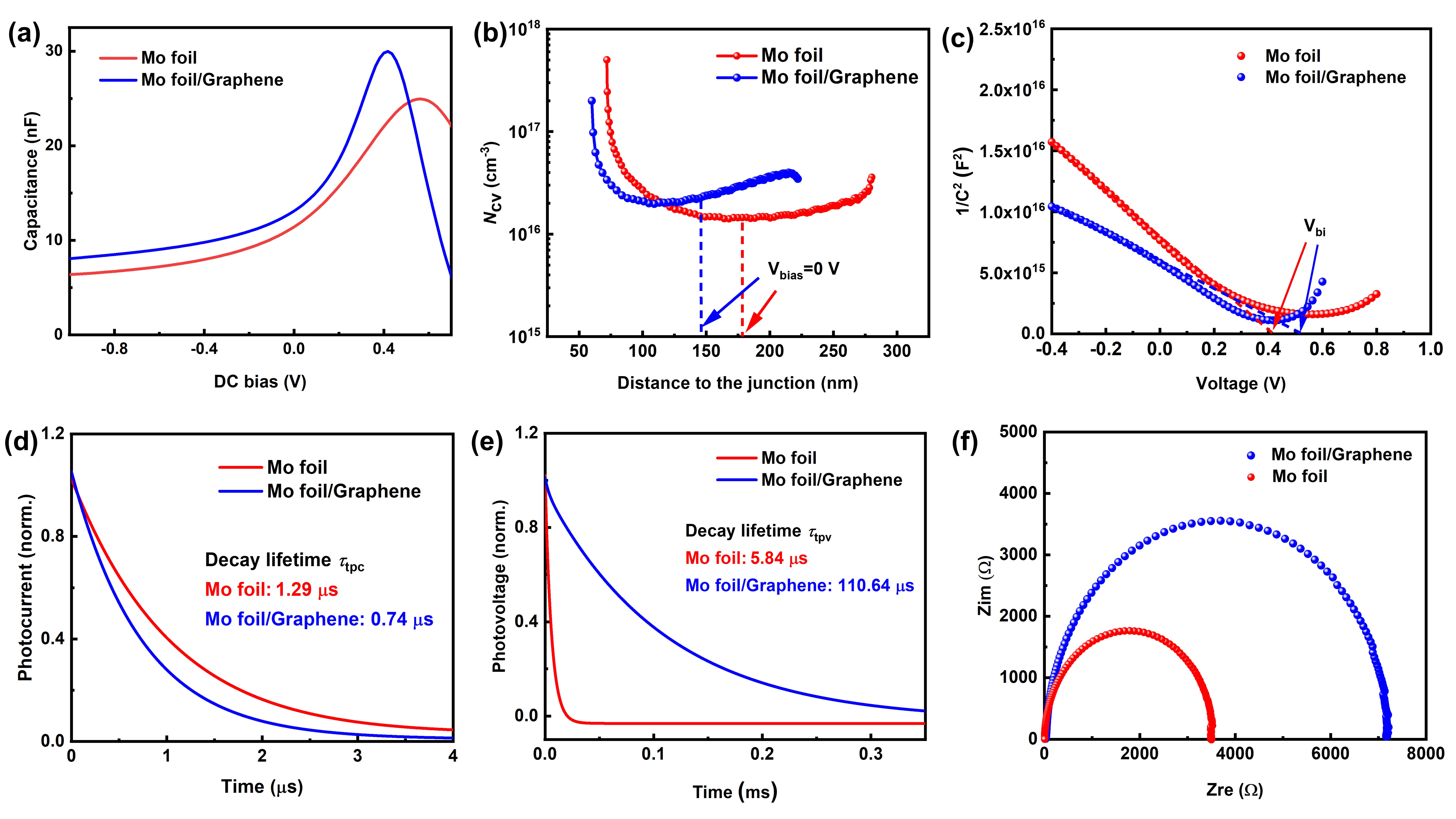
The carrier collection within two devices was investigated by conducting Capacity-voltage (C-V) and charge dynamics analysis to elucidate the underlying device physics. Capacity-voltage (C-V) and derived depletion region width are shown in Figure 5. With enhanced crystallinity and phase purity at the bottom region of the absorber, the carrier density derived from C-V has been improved from cm-3 to cm-3, which might contribute to enhanced conductivity. The depletion region was changed from 178.9 nm to 145.66 nm, suggesting reduced recombination losses. A larger built-in potential of around 0.51 V is the reason for higher open-circuit voltage and overall efficiency 27.
Transient photocurrent (TPC) and transient photovoltage (TPV) measurements are used to investigate the charge transfer and recombination characteristics of the two devices. TPC measures the decay of photocurrent in a closed circuit, reflecting the transport properties of photogenerated carriers in the device, while TPV measures the decay of photovoltage in an open circuit, indicating recombination properties. From TPV decay, the charge recombination lifetime () is determined. The values for Mo foil and Mo foil/Graphene devices are 5.84 and 110.64 s, respectively, showing better recombination suppression in the Mo foil/Graphene device. Similarly, TPC decay gives the charge transfer lifetime (), indicating the time for carriers to reach the electrode. The values for Mo foil and Mo foil/Graphene devices are 1.29 and 0.74 s, respectively, implying improved charge transport capability in the Mo foil/Graphene device. Therefore, the insertion of graphene enhances both carrier recombination suppression and transport in CZTSSe films.
| Device |
|
|
|
|
|
|
||||||||||||
|---|---|---|---|---|---|---|---|---|---|---|---|---|---|---|---|---|---|---|
| Mo foil | 0.41 | 178.90 | 5.84 | 1.29 | 3.53 | |||||||||||||
| Mo foil/G | 0.51 | 145.66 | 110.64 | 0.74 | 7.17 |
Moreover, electrochemical impedance spectroscopy (EIS) was conducted to analyze the carrier recombination behavior. The Nyquist diagrams of EIS spectra and equivalent circuit diagrams of the devices are described in Figure 5(f). The intersection points of high and low frequency with the x-axis are the series resistance (Rs) and recombination resistance (Rrec), respectively, while the shunt resistance (Rsh) is represented by the diameter of the impedance spectrum circle line. The Rrec values of the Mo foil and Mo foil/Graphene devices are 3.53 and 7.1 K respectively. The smaller Rrec of the Mo foil/Graphene device is consistent with the TPV result, leading to effective suppression of defect recombination at the interface.
2.1 Conclusion
In this work, we investigated the impact of inserting graphene layers at the Mo foil/CZTSSe interface and studied their influences on CZTSSe grain growth and the performance of flexible CZTSSe solar cells. Samples with a graphene interlayer show a smoother and denser morphology, with significantly improved crystallinity of CZTSSe. The champion flexible CZTSSe thin-film device, incorporating a graphene back-interface passivation layer, achieved a conversion efficiency of 9.41%, an open-circuit voltage of 0.48V, a short-circuit current density of 33.64 mA/cm2 and a fill factor of 58.12%.
Detailed analysis revealed that the insertion of the graphene not only influenced the grain growth on the Mo foil substrate but also prohibited the phase decomposition at the nanoscale of the back contact and the bottom region of the absorbers. Defects within absorbers were significantly passivated due to enhanced crystallinity. Carrier collection at the back contact was more effective with better physical contact built by the inserted graphene. A lower potential barrier was obtained, facilitating hole transport and mitigating the reverse diode effect at the back interface, leading to the formation of quasi-ohmic contact at the back contact.
References
- Wang et al. 2021 Wang, F.; Harindintwali, J. D.; Yuan, Z.; Wang, M.; Wang, F.; Li, S.; Yin, Z.; Huang, L.; Fu, Y.; Li, L.; others Technologies and perspectives for achieving carbon neutrality. The Innovation 2021, 2
- Pagliaro et al. 2008 Pagliaro, M.; Ciriminna, R.; Palmisano, G. Flexible solar cells. ChemSusChem: Chemistry & Sustainability Energy & Materials 2008, 1, 880–891
- Deng et al. 2021 Deng, H.; Sun, Q.; Yang, Z.; Li, W.; Yan, Q.; Zhang, C.; Zheng, Q.; Wang, X.; Lai, Y.; Cheng, S. Novel symmetrical bifacial flexible CZTSSe thin film solar cells for indoor photovoltaic applications. Nature communications 2021, 12, 3107
- Yang et al. 2019 Yang, K.-J.; Kim, S.; Kim, S.-Y.; Ahn, K.; Son, D.-H.; Kim, S.-H.; Lee, S.-J.; Kim, Y.-I.; Park, S.-N.; Sung, S.-J.; others Flexible Cu2ZnSn (S, Se) 4 solar cells with over 10% efficiency and methods of enlarging the cell area. Nature communications 2019, 10, 2959
- Yan et al. 2022 Yan, Q.; Sun, Q.; Deng, H.; Xie, W.; Zhang, C.; Wu, J.; Zheng, Q.; Cheng, S. Enhancing carrier transport in flexible CZTSSe solar cells via doping Li strategy. Journal of Energy Chemistry 2022, 75, 8–15
- Li et al. 2023 Li, J.; Sun, K.; Yuan, X.; Huang, J.; Green, M. A.; Hao, X. Emergence of flexible kesterite solar cells: Progress and perspectives. npj Flexible Electronics 2023, 7, 16
- Hamtaei et al. 2023 Hamtaei, S.; Brammertz, G.; Poortmans, J.; Vermang, B. A review on barrier layers used in flexible stainless-steel based CIGS photovoltaic devices. npj Flexible Electronics 2023, 7, 36
- Xu et al. 2023 Xu, X.; Zhou, J.; Yin, K.; Wang, J.; Lou, L.; Li, D.; Shi, J.; Wu, H.; Luo, Y.; Meng, Q. 12.84% Efficiency flexible kesterite solar cells by heterojunction interface regulation. Advanced Energy Materials 2023, 13, 2301701
- Yang et al. 2021 Yang, K.-J.; Kim, S.; Kim, S.-Y.; Son, D.-H.; Lee, J.; Kim, Y.-I.; Sung, S.-J.; Kim, D.-H.; Enkhbat, T.; Kim, J.; others Sodium effects on the diffusion, phase, and defect characteristics of kesterite solar cells and flexible Cu2ZnSn (S, Se) 4 with greater than 11% efficiency. Advanced Functional Materials 2021, 31, 2102238
- Yang et al. 2024 Yang, W.; Ji, Y.; Chen, W.; Pan, Y.; Chen, Z.; Wu, S.; Russo, S. P.; Xu, Y.; Smith, T. A.; Chesman, A.; others The Multiple Roles of Na Ions in Highly Efficient CZTSSe Solar Cells. Small 2024, 2307807
- Yazici et al. 2015 Yazici, S.; Olgar, M. A.; Akca, F. G.; Cantas, A.; Kurt, M.; Aygun, G.; Tarhan, E.; Yanmaz, E.; Ozyuzer, L. Growth of Cu2ZnSnS4 absorber layer on flexible metallic substrates for thin film solar cell applications. Thin Solid Films 2015, 589, 563–573
- Sun et al. 2018 Sun, K.; Liu, F.; Huang, J.; Yan, C.; Song, N.; Sun, H.; Xue, C.; Zhang, Y.; Pu, A.; Shen, Y.; others Flexible kesterite Cu2ZnSnS4 solar cells with sodium-doped molybdenum back contacts on stainless steel substrates. Solar Energy Materials and Solar Cells 2018, 182, 14–20
- Todorov et al. 2015 Todorov, T.; Olenick, J.; AOlenick, K.; Gunawan, O.; Gershon, T.; Sturdevant, C.; Lee, Y. S.; Chang, L.-y.; Guha, S. Flexible kesterite solar cells on ceramic substrates for advanced thermal processing. 2015 IEEE 42nd Photovoltaic Specialist Conference (PVSC). 2015; pp 1–3
- Lundberg et al. 2005 Lundberg, O.; Edoff, M.; Stolt, L. The effect of Ga-grading in CIGS thin film solar cells. Thin Solid Films 2005, 480, 520–525
- Hsiao and Sites 2012 Hsiao, K.-J.; Sites, J. R. Electron reflector to enhance photovoltaic efficiency: application to thin-film CdTe solar cells. Progress in Photovoltaics: Research and Applications 2012, 20, 486–489
- Sharbati et al. 2018 Sharbati, S.; Gharibshahian, I.; Orouji, A. A. Proposed suitable electron reflector layer materials for thin-film CuIn1- xGaxSe2 solar cells. Optical Materials 2018, 75, 216–223
- Giraldo et al. 2018 Giraldo, S.; Saucedo, E.; Neuschitzer, M.; Oliva, F.; Placidi, M.; Alcobé, X.; Izquierdo-Roca, V.; Kim, S.; Tampo, H.; Shibata, H.; others How small amounts of Ge modify the formation pathways and crystallization of kesterites. Energy & Environmental Science 2018, 11, 582–593
- Yan et al. 2017 Yan, C.; Sun, K.; Liu, F.; Huang, J.; Zhou, F.; Hao, X. Boost Voc of pure sulfide kesterite solar cell via a double CZTS layer stacks. Solar Energy Materials and Solar Cells 2017, 160, 7–11
- Scragg et al. 2012 Scragg, J. J.; Watjen, J. T.; Edoff, M.; Ericson, T.; Kubart, T.; Platzer-Bjorkman, C. A detrimental reaction at the molybdenum back contact in Cu2ZnSn (S, Se) 4 thin-film solar cells. Journal of the American Chemical Society 2012, 134, 19330–19333
- Suk et al. 2011 Suk, J. W.; Kitt, A.; Magnuson, C. W.; Hao, Y.; Ahmed, S.; An, J.; Swan, A. K.; Goldberg, B. B.; Ruoff, R. S. Transfer of CVD-grown monolayer graphene onto arbitrary substrates. ACS nano 2011, 5, 6916–6924
- Graf et al. 2007 Graf, D.; Molitor, F.; Ensslin, K.; Stampfer, C.; Jungen, A.; Hierold, C.; Wirtz, L. Spatially resolved Raman spectroscopy of single-and few-layer graphene. Nano letters 2007, 7, 238–242
- Su et al. 2020 Su, Z.; Liang, G.; Fan, P.; Luo, J.; Zheng, Z.; Xie, Z.; Wang, W.; Chen, S.; Hu, J.; Wei, Y.; others Device postannealing enabling over 12% efficient solution-processed Cu2ZnSnS4 solar cells with Cd2+ substitution. Advanced Materials 2020, 32, 2000121
- Liu et al. 2017 Liu, F.; Yan, C.; Sun, K.; Zhou, F.; Hao, X.; Green, M. A. Light-bias-dependent external quantum efficiency of kesterite Cu2ZnSnS4 solar cells. ACS Photonics 2017, 4, 1684–1690
- Ji et al. 2023 Ji, Y.; Zhao, X.; Pan, Y.; Su, Z.; Lin, J.; Akinoglu, E. M.; Xu, Y.; Zhang, H.; Zhao, P.; Dong, Y.; others CuSCN modified back contacts for high performance CZTSSe solar cells. Advanced Functional Materials 2023, 33, 2211421
- Hsiao et al. 2013 Hsiao, K.-J.; Liu, J.-D.; Hsieh, H.-H.; Jiang, T.-S. Electrical impact of MoSe 2 on CIGS thin-film solar cells. Physical Chemistry Chemical Physics 2013, 15, 18174–18178
- Yoon et al. 2014 Yoon, J.-H.; Kim, J.-H.; Kim, W. M.; Park, J.-K.; Baik, Y.-J.; Seong, T.-Y.; Jeong, J.-h. Electrical properties of CIGS/Mo junctions as a function of MoSe2 orientation and Na doping. Progress in Photovoltaics: Research and Applications 2014, 22, 90–96
- Ji et al. 2024 Ji, Y.; Chen, W.; Yan, D.; Bullock, J.; Xu, Y.; Su, Z.; Yang, W.; Laird, J. S.; Zheng, T.; Wu, N.; others An ITO-Free Kesterite Solar Cell. Small 2024, 20, 2307242