Understanding field-free single-shot laser-induced reversal of exchange bias
Abstract
Exchange bias is applied ubiquitously throughout the spintronics industry for its ability to provide a reference direction robust to external magnetic field disturbances. For some applications, reorienting the exchange-biased reference axis may add to or enhance functionality of devices. Conventional methods for achieving this reorientation require assisting magnetic fields with long setting times and are thus limited in terms of speed and versatility. In this study, we show that by integrating functionalized materials (\chCo/\chGd multilayers) into an existing thin film stack (\chPt/\chCo/\chIrMn), perpendicular exchange bias can be reoriented by exciting it with a single femtosecond laser pulse, without an external field and on an ultrafast timescale. We found this effect to be repeatable arbitrarily many times, with only the first laser pulse incurring a loss of the initial exchange bias magnitude, yet preserving the unidirectionality required for referencing. By combining an experimental mapping of three key parameters (stack, laser and magnetic field properties) with microscopic models we were able to unravel the processes and features of the exchange bias reversal by considering the relevance of Curie, Néel and blocking temperatures. The outcomes of this study provide guiding principles towards designing fully optically reprogrammable magnetic sensing devices.
I Introduction
At the interface between an antiferromagnet and a ferromagnet, exchange coupling may induce a unidirectional anisotropy that pins the magnetization in the ferromagnet [1, 2]. This phenomenon, known as exchange bias, is a fundamental ingredient in state-of-the-art magnetic memory elements and spintronic sensors, where it defines a reference axis that is robust against external magnetic field perturbations [3]. In spintronic sensors, each element has its own exchange bias-induced reference axis, programmed during the fabrication process by oven annealing: the entire chip is heated above the blocking temperature (where exchange bias vanishes) and cooled down in the presence of a magnetic field, saturating the ferromagnetic layers and uniformly setting the exchange bias.
Most high-sensitivity magnetic sensors nowadays are laid out in a Wheatstone bridge configuration [4] connecting sensors with reversed reference axes. Also, multiaxial sensors consist of elements with rotated reference axes. For such designs, the global character of oven annealing makes it unsuitable for reference setting, illustrating the need for more advanced fabrication techniques that manipulate the pinning direction of individual sensing elements. Here, local annealing methods by laser heating [5, 6, 7] or Joule heating [8, 9] are advantageous and hence they constitute the motivation for our present study. The novelty of our approach lies in the ability to repin fully unidirectionally without external magnetic fields. Other methods exist that directly act on the antiferromagnet (by spin-orbit torques [10, 11] or strain [12, 13]) or physically change the reference orientation of individual sensors by placement on self-assembling structures [14, 15], though these designs deviate quite strongly from any existing architecture.
To realize a field-free and ultrafast repinning of exchange bias, we combined the laser annealing technique [5] with work on all-optical helicity-independent magnetization switching (AOS) [16, 17, 18]. AOS was first observed in perpendicularly magnetized ferrimagnets of transition metals (\chFe and/or \chCo) alloyed with the rare-earth element \chGd, where an ultrashort (femtosecond) laser pulse toggle-switches the magnetization for sufficiently energetic pulses [16, 17]. Guo et al. [19] were the first to demonstrate that when such alloys are exchange biased by antiferromagnetic \chIr_0.2Mn_0.8, a single laser pulse reverses both the magnetization and the exchange bias, although only to a limited extent ( or less) and losing the unidirectionality of the pinned layer. Here, we study exchange bias reversal in structures containing synthetic ferrimagnets (i.e. multilayers of \chCo and \chGd). Synthetic ferrimagnets show promising performance benefits compared to their alloy counterparts [18, 20] and have demonstrable potential for application in spintronic memory devices [21, 22].
In this work, we demonstrate the potential of AOS for enhancing sensor functionality by integrating synthetic ferromagnets into an existing spin valve architecture and provide guidelines for performance optimization. Our methodology consists of an experimentally obtained data set exploring a three-dimensional phase space described in section II, along with microscopic models treating the processes taking place at various timescales and providing deeper insight into the underlying mechanisms. Our results are presented and discussed in section III. Finally, in section IV we will give a brief perspective on the capabilities and limitations of our proposal.
II Methodology
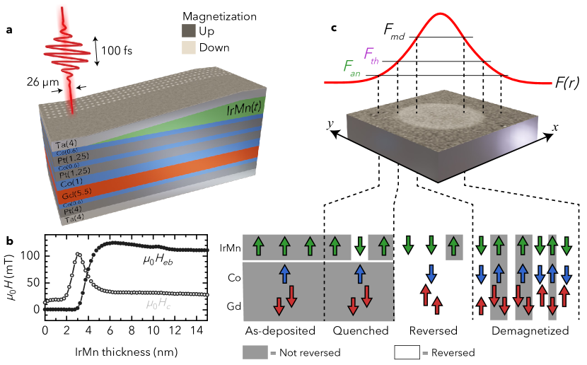
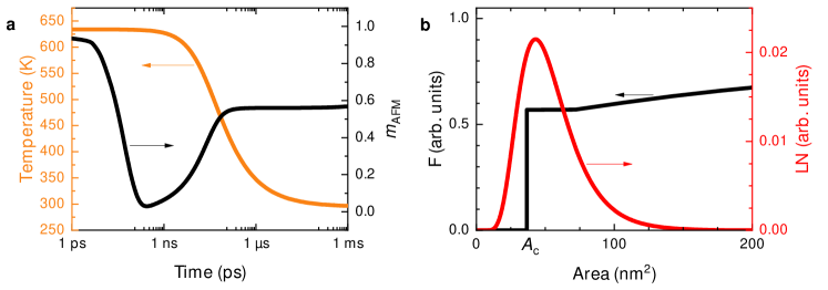
Samples are prepared with DC magnetron sputtering deposition at a base pressure of . A shutter situated between the target and the substrate was moved at constant speed during the deposition of \chIr_0.2Mn_0.8 to create a linear thickness gradient across the sample. The stacks consist of \chTa(4)/\chPt(4)/\chCo(0.6)/\chGd(5.5)/\chCo(1)/[\chPt(1.25)/\chCo(0.6)]x2/\chIrMn()/\chTa(5) grown on thermally oxidized \chSi/\chSiO2(100) substrates (thicknesses in nanometers, see Fig. 1a). All layers are deposited in the presence of a static field. This ensures an exchange bias of up to is set by the \chCo during deposition (as a function of \chIrMn thickness, see Fig. 1b) and eliminates the need for post-annealing. There are two main reasons we purposefully avoid annealing. Firstly, annealing these stacks is likely to result in heavy diffusion of the mobile \chGd atoms [23]. Secondly, annealing would enlarge the antiferromagnetic grains, making them more stable and ultimately less susceptible to reversal. The \chPt/\chCo layers serve as a buffer preventing the \chGd from contaminating the \chCo/\chIrMn interface and compromising the exchange bias. More details about stack considerations are provided in section S1.
In our experiments, the films were subjected to one or more Gaussian laser pulses (pulse length at half maximum, wavelength) focused onto the sample at normal incidence (spot diameter at half maximum, see section S2). Sweeping the position along the \chIrMn wedge allowed us to parameterize the \chIrMn thickness, as is illustrated in Fig. 1a. Furthermore, we parameterized the peak intensity of the Gaussian laser pulse (by means of a neutral density filter) and the magnitude of a constant magnetic field perpendicular to the sample plane (using the field as a tool to influence the AOS process), amounting to a three-dimensional phase space. Characterization of the exchange bias was carried out using Kerr microscopy, with which (-)-loops were measured all throughout the spatial extent of the switched region, as shown in Fig. 1c. The effective exchange bias field distribution is then extracted from the shift in the (-)-loops. Relating the position back to the intensity distribution of the Gaussian laser pulse allowed us to investigate the behavior of the exchange bias reversal as a function of the laser fluence. This procedure is repeated for all spots, amounting to a total of 3.4 million hysteresis loops that were processed.
For exchange bias setting, slow processes occurring on timescales much longer than the femtosecond pulse duration cannot be ignored. Thus, in order to deepen our understanding of the underlying physical mechanisms of the reversal and thereby identifying the parameters that can be optimized, we developed a model bridging processes that are happening at both ultrashort and longer timescales (details can be found in section S3). The first regime (within after laser incidence) is described by the layered microscopic three-temperature model (M3TM) framework for modeling AOS of the ferromagnetic layers [24, 20]. This reversal is propagated from the \chCo/\chGd layers to the \chIrMn layer via interlayer exchange coupling, which approximately takes place in the first .
In the second temporal regime of the simulation, the exchange bias setting is modeled with an Arrhenius description [25]. The antiferromagnet is modeled as a collection of non-interacting grains with distributed volumes and uniform Néel vectors and anisotropies. Using an attempt frequency of , the rate at which a grain will reverse its orientation is calculated via Arrhenius’ equation as
| (1) |
where is the Boltzmann constant and is the energy barrier for Néel vector reversal depending on the anisotropy and exchange interaction. Both those latter quantities also have underlying dependencies on the temperature evolution , leading to a large expected importance of on the setting fraction. The simulation lasts until has relaxed back to room temperature.
Separating the M3TM from the Arrhenius model allows us to distinguish between the exchange-driven and thermally-assisted regimes and inspect what the influence of each is on the total reversal process.
III Results and discussion
A typical experimental example of field-free single-pulse exchange bias reversal, similar to Guo et al.[19], is shown in Fig. 2
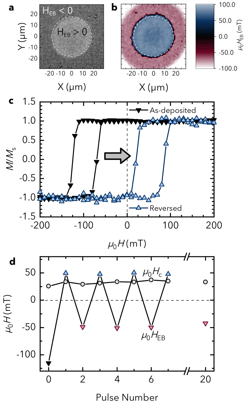
for our optimized stacks. Fig. 2a depicts a Kerr microscopy image of the magnetic state after laser excitation in field-free conditions. The same spot is shown in Fig. 2b, where the exchange bias field is extracted at each location from the local hysteresis loop, two examples of which are shown in Fig. 2c: one with laser excitation (measured within the spot at a radius corresponding to a fluence of ) and one without laser excitation (measured far away from the spot). From Fig. 2c it is readily observed that the exchange bias sign was reversed from negative to positive. More notably, the remanent state at remains unidirectional, meaning only one state of (up or down) is stable at zero field, and (crucially for application in referencing) if it was up before the laser pulse it will be down after the laser pulse (and vice versa). Moreover, we confidently state that indeed AOS in the \chCo/\chGd layer successfully propagates to the \chCo/\chPt layers and ultimately drives the exchange bias reversal.
Figure 2c also illustrates that the magnitude of exchange bias is significantly reduced after the single-pulse laser excitation, even under the most optimal conditions. The maximum retention of magnitude we observed for as-deposited films was (Fig. 2b), which outperforms the record found in CoGd alloys[26]. The origin of the magnitude reduction can be understood by considering the granular nature of the antiferromagnet. Grains are present in various sizes, and smaller grains are more probable to reorient themselves during the laser excitation because they have a lower energy barrier to overcome. In the as-deposited state however, the exchange bias is set at room temperature with an external field aligning all grains in the same direction, thus not accounting for the probabilistic nature of grain reversal. This explains why the magnitude of exchange bias is reduced upon laser excitation.
In addition, this interpretation predicts a repeatable reversal process without degradation upon successive laser pulses. This we investigated by firing repeated laser pulses at the same spot on the sample. As a function of the number of pulses, it was observed that only the first pulse induces a loss of , after which successive pulses toggle between two stable states (see Fig. 2d). For this sample we tested the stability up to successive switches and it always retains the unidirectionality condition . This is an important observation for applications whose operation may rely on continuous repeated toggle switches.
III.1 Fluence dependence of reversal
One key parameter we can control to shed more light on the underlying reversal mechanism is the intensity of the laser pulse, characterized by its fluence (energy per pulse per unit area). At constant pulse length, the fluence determines the temperature evolution in the layers. Whether or not the system temperature then exceeds certain critical temperatures (like Curie, blocking or Néel temperatures) and for how long those temperatures are exceeded influences how the magnetic state dynamically evolves. For exchange bias reversal, where various critical temperatures play a role, a very rich fluence dependence can then be expected.
From heat maps such as shown in Fig. 2b, the dependence of exchange bias reversal on pulse energy can be extracted. This is shown in Fig. 3a
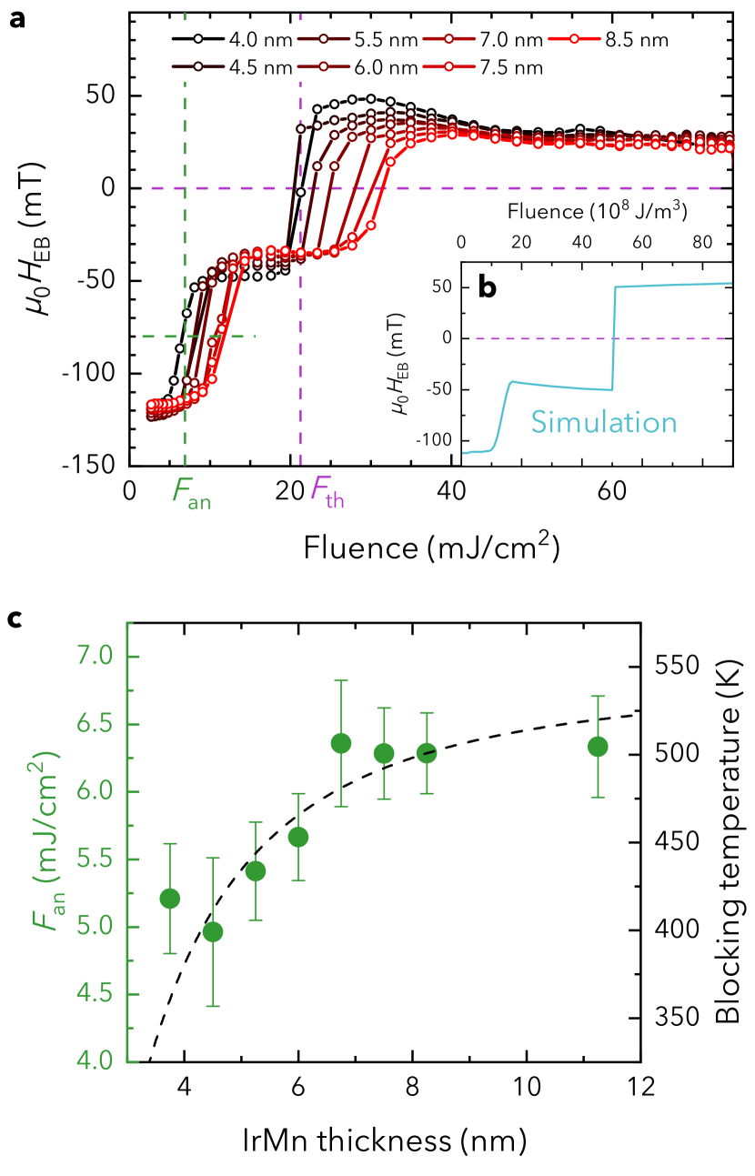
for various thicknesses of the \chIrMn layer. Over the range of fluences investigated we did not observe a monotonic increase of the exchange bias magnitude with increasing fluence. Rather, regions of both increasing and decreasing trends appear in the fluence dependence of (n.b. verified to indeed scale with the local fluence level and not the overall pulse energy).
A number of important conclusions can be drawn from the fluence dependence in Fig. 3a. First of all, two plateaus can be distinguished: one located around and the other appearing for fluences above . This behavior can be understood as follows. The critical temperature of bulk \chIrMn is approximately , while for bulk \chCo it is . This means that as the fluence is increased, the first critical temperature to be overcome by the electron temperature is that of the antiferromagnet, resulting in a quasi-annealing effect. In Fig. 3a this is represented by the threshold and a decrease in magnitude of from around to . Only when the fluence is further increased the exchange bias will be reversed through zero, as at that point the threshold fluence for switching the ferromagnetic layers is overcome. The simulations reproduce all these features, as shown in Fig. 3b. Furthermore, based on the simulations we understand the broadening of the transition in around as a consequence of the grain size distribution, allowing smaller grains to reverse already at lower fluences than larger grains. No such broadening is observed around since AOS only has a binary outcome. Note also that the magnitude of above and below is always equal, for both the experiment as well as the simulation.
The results from Guo et al.[19] fit this picture: they lack the plateau at since their systems do not contain \chPt/\chCo multilayers (only a ferrimagnet with a lower expected Curie temperature) and their stacks are reversed (with \chIrMn on the bottom), leading to a situation where . To further back up our claims, section III.2 investigates the effects of magnetic fields applied during the switch. These should only have an effect on the ferromagnets and leave the antiferromagnet unaffected.
A second observation can be made about the absolute threshold fluences which are shifted as the antiferromagnetic thickness is increased. Since we illuminate from the top, it is expected that the threshold fluence for switching the ferromagnets increases exponentially with antiferromagnetic thickness due to skin-depth effects in the \chIrMn. By fitting this exponential increase we corrected the data of the antiferromagnetic threshold to filter out the skin-depth contribution (see section S4). The corrected data, shown in Fig. 3c, is clearly not monotonic, but rather it saturates at around . This behavior corresponds nicely with the dependence of blocking temperature on \chIrMn thickness, that we separately measured and also plotted in Fig. 3c (section S5). This further indicates that indeed is related to a transition in the antiferromagnet.
III.2 Magnetic field dependence of reversal
Besides laser fluence, the second key parameter in our investigation is the influence of an external magnetic field on the exchange bias reversal. We distinguish here between assisting fields (that promote the reversal of ) and hindering fields (that stabilize the as-deposited ). A study by Peeters et al. [27] on \chCo/\chGd bilayers demonstrated that a hindering field will greatly influence the AOS dynamics on the longer timescales, i.e., after the initial few picoseconds in which the magnetization reversal takes place. In particular: the larger the hindering field, the shorter the time spent in the reversed state before remagnetizing in the original direction. By changing the magnitude of the field, this time period can be continuously varied from infinite at to at hindering field and beyond to even shorter timescales at larger fields.
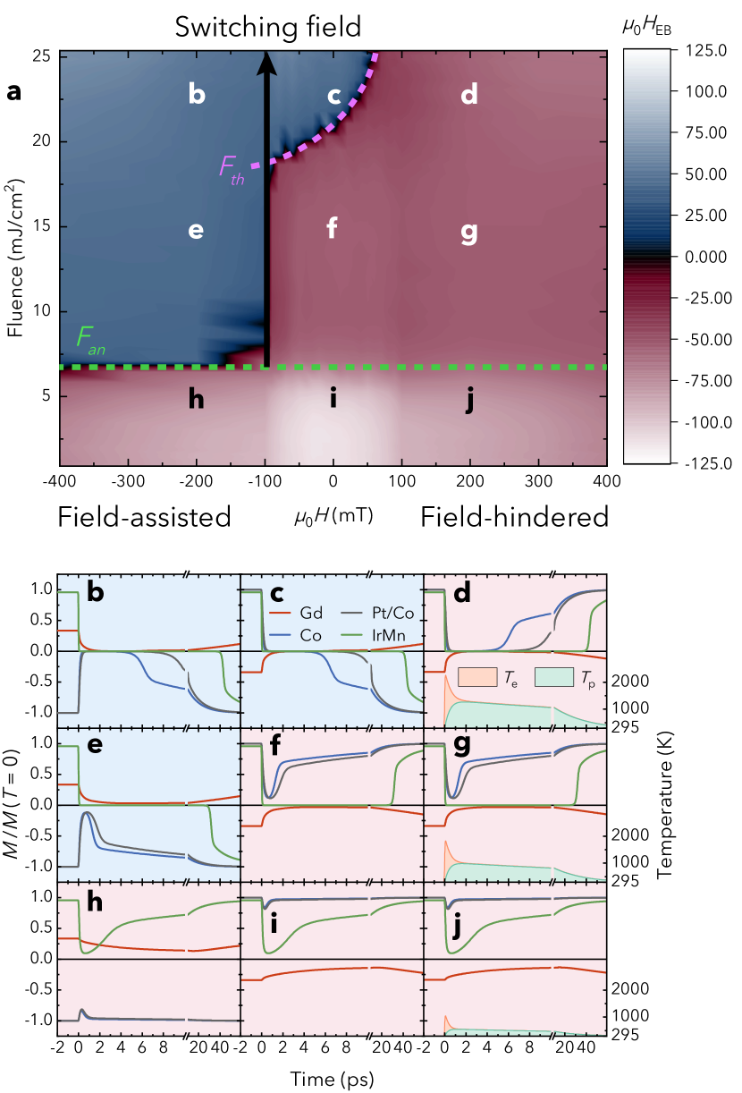
Figure 4a shows how experimentally the external field influences the exchange bias reversal for . For some interesting points in the phase diagram the corresponding simulated M3TM traces of the magnetization are shown in Fig. 4b-j. As is expected, for large magnitudes (positive or negative) the exchange bias is quasi-annealed by the external field. The point at which the transition takes place is determined by the switching field required to overcome and the coercivity. Compare for example the simulated time traces in Fig. 4e and 4g (see S3 for details on the implementation).
As was mentioned in section III.1, the use of magnetic fields allows us to distinguish between thresholds relating to the ferromagnet and the antiferromagnet. As is readily observed in Fig. 4a, the threshold at around is independent of the field, confirming that this signifies the peak temperature exceeding the Néel temperature of the antiferromagnet. This also follows from simulations (Fig. 4h, 4i and 4j), where below this threshold the electron temperature will not exceed the critical temperature of the antiferromagnet, which thus remagnetizes in the original direction (green lines in Fig. 4b-j). On the other hand, the threshold boundary at is highly dependent on the field. Its shape corresponds to what was predicted by Peeters et al.[27], i.e., an increase of the AOS threshold fluence for large enough hindering fields. This provides more evidence for our interpretation of being an annealing threshold and being an AOS threshold.
The simulated temperature evolution for the electron () and phonon () baths are plotted for three different fluence values in panels 4d, 4g and 4j. The \chGd layers, having a Curie temperature below room temperature, only obtain an induced magnetization from the interface with \chCo, hence the lower magnitude of the red lines in Fig. 4b-j. It can also be seen that the ferromagnetic layers (blue for \chCo and gray for \chPt/\chCo) are initialized differently in panels 4b, 4e and 4h to mimic the effect of the switching field. The green lines for \chIrMn, representing the Néel vector, are not reversed by fluences below (panels 4h-j) because does not exceed the Néel temperature. When a large enough field is applied, the ferromagnetic layers will tend to align with it and drag the \chIrMn along, bringing the \chIrMn in the switched state for assisting fields (panels 4b and 4e) and in the original state for hindering fields (panels 4d and 4g). In the field-free case, a distinction is made between fluences below the AOS threshold (panel 4f) where no reversal takes place, and fluences above (panel 4c) where AOS takes place and the antiferromagnet is switched as well. All in all, the simulations thus qualitatively reproduce all features from the experimental data in Fig. 4a, giving us confidence in our interpretation of the behavior on the ultrafast timescales.
IV Conclusion and outlook
In conclusion, we have demonstrated the field-free ultrafast reversal of exchange bias in our optimized stacks upon excitation with a single femtosecond laser pulse. It was revealed that the magnitude of reduces upon the first pulse, but is maintained upon successive pulses. This gives us confidence that the technique is suitable for application in functional devices. We explored a phase space of three parameters (antiferromagnetic layer thickness, laser fluence and applied magnetic field), both experimentally and with simulations. Each provided us with insight into the mechanisms responsible for reversal. We distinguished two threshold fluences in the reversal process: one for the critical temperature of the \chIrMn and one for that of the \chCo/\chGd. This picture tells us that ideally these two thresholds should be engineered to be as close together as possible. That way, the span of the fluence regime where is reversed is optimized. Secondly, the temperature evolution towards ambient conditions is of great importance for the fraction of that is retained. Ideally, the temperature relaxes relatively quickly through the critical temperature of the antiferromagnet and then lingers at a slightly less elevated temperature, such that unswitched grains have the tendency to move to a lower energy level where they are reversed, while switched grains have insufficient thermal energy to reorient themselves.
For future work, integration of \chCo/\chGd systems in functional spin valve devices is considered a promising approach for reference axis reorientation. Based on our findings, special attention should be given to engineering the heat management of the devices, e.g. by incorporating heat sinks or insulators and by tuning the geometry. Especially \chGd may pose a challenge in this regard, as it is known to be subject to rapid degradation [28]. Some limitations are lifted however when transitioning to in-plane magnetized systems, as having strong perpendicular anisotropy is no longer a requirement. It is therefore conceived that the technique presented in this work has potential for innovating spintronic sensing devices.
Acknowledgements.
This work is financially supported by the Eindhoven Hendrik Casimir Institute. Paper was written by FvR, SV performed and analyzed the blocking temperature measurements, BK and DL supervised the work and revised the paper.References
- Meiklejohn [1962] W. H. Meiklejohn, “Exchange Anisotropy-A Review,” Journal of Applied Physics 33, 1328–1335 (1962).
- Nogués and Schuller [1999] J. Nogués and I. K. Schuller, “Exchange bias,” Journal of Magnetism and Magnetic Materials 192, 203–232 (1999).
- Freitas, Ferreira, and Cardoso [2016] P. P. Freitas, R. Ferreira, and S. Cardoso, “Spintronic Sensors,” Proceedings of the IEEE 104, 1894–1918 (2016).
- Freitas et al. [1999] P. P. Freitas, J. L. Costa, N. Almeida, L. V. Melo, F. Silva, J. Bernardo, and C. Santos, “Giant magnetoresistive sensors for rotational speed control,” Journal of Applied Physics 85, 5459–5461 (1999).
- Berthold et al. [2014] I. Berthold, U. Löschner, J. Schille, R. Ebert, and H. Exner, “Exchange Bias Realignment Using a Laser-based Direct-write Technique,” Physics Procedia 56, 1136–1142 (2014).
- Almeida et al. [2015] M. Almeida, P. Matthes, O. Ueberschär, M. Müller, R. Ecke, H. Exner, M. Albrecht, and S. Schulz, “Optimum Laser Exposure for Setting Exchange Bias in Spin Valve Sensors,” Physics Procedia 75, 1192–1197 (2015).
- Ueberschar et al. [2015] O. Ueberschar, M. J. Almeida, P. Matthes, M. Muller, R. Ecke, R. Ruckriem, J. Schuster, H. Exner, and S. E. Schulz, “Optimized Monolithic 2-D Spin-Valve Sensor for High-Sensitivity Compass Applications,” IEEE Transactions on Magnetics 51, 1–4 (2015).
- Cao and Freitas [2010] J. Cao and P. P. Freitas, “Wheatstone bridge sensor composed of linear MgO magnetic tunnel junctions,” Journal of Applied Physics 107, 09E712 (2010).
- Wang et al. [2024] W. Wang, Y. Chen, B. Wang, L. Wang, Y. Han, W. Su, Z. Hu, Z. Wang, and M. Liu, “Locally Reconfigurable Exchange Bias for Tunable Spintronics by Pulsed Current Injection,” physica status solidi (RRL) – Rapid Research Letters 18 (2024), 10.1002/pssr.202300303.
- Wang et al. [2022a] Y. Wang, T. Taniguchi, P. H. Lin, D. Zicchino, A. Nickl, J. Sahliger, C. H. Lai, C. Song, H. Wu, Q. Dai, and C. H. Back, “Time-resolved detection of spin-orbit torque switching of magnetization and exchange bias,” Nature Electronics 5, 840–848 (2022a).
- Chen et al. [2023] W. Chen, Y. Lin, K. Zhang, Z. Cao, X. Zhao, Z. Zhou, X. Wang, S. Yan, H. Du, Q. Leng, and S. Yan, “Spin Orbit Torque Locally Controlling Exchange Bias to Realize High Detection Sensitivity of Two-dimensional Magnetic Field,” Fundamental Research (2023), 10.1016/j.fmre.2023.07.010.
- Su et al. [2020] W. Su, Z. Wang, Y. Chen, X. Zhao, C. Hu, T. Wen, Z. Hu, J. Wu, Z. Zhou, and M. Liu, “Reconfigurable Magnetoresistive Sensor Based on Magnetoelectric Coupling,” Advanced Electronic Materials 6 (2020), 10.1002/aelm.201901061.
- Wang et al. [2023] M. Wang, M. Li, Y. Lu, X. Xu, and Y. Jiang, “Electric field controlled perpendicular exchange bias in Ta/Pt/Co/IrMn/Pt heterostructure,” Applied Physics Letters 123 (2023), 10.1063/5.0160957.
- Becker et al. [2019] C. Becker, D. Karnaushenko, T. Kang, D. D. Karnaushenko, M. Faghih, A. Mirhajivarzaneh, and O. G. Schmidt, “Self-assembly of highly sensitive 3D magnetic field vector angular encoders,” Science Advances 5 (2019), 10.1126/sciadv.aay7459.
- Becker et al. [2022] C. Becker, B. Bao, D. D. Karnaushenko, V. K. Bandari, B. Rivkin, Z. Li, M. Faghih, D. Karnaushenko, and O. G. Schmidt, “A new dimension for magnetosensitive e-skins: active matrix integrated micro-origami sensor arrays,” Nature Communications 13 (2022), 10.1038/s41467-022-29802-7.
- Radu et al. [2011] I. Radu, K. Vahaplar, C. Stamm, T. Kachel, N. Pontius, H. A. Dürr, T. A. Ostler, J. Barker, R. F. L. Evans, R. W. Chantrell, A. Tsukamoto, A. Itoh, A. Kirilyuk, T. Rasing, and A. V. Kimel, “Transient ferromagnetic-like state mediating ultrafast reversal of antiferromagnetically coupled spins,” Nature 472, 205–208 (2011).
- Ostler et al. [2012] T. Ostler, J. Barker, R. Evans, R. Chantrell, U. Atxitia, O. Chubykalo-Fesenko, S. El Moussaoui, L. Le Guyader, E. Mengotti, L. Heyderman, F. Nolting, A. Tsukamoto, A. Itoh, D. Afanasiev, B. Ivanov, A. Kalashnikova, K. Vahaplar, J. Mentink, A. Kirilyuk, T. Rasing, and A. Kimel, “Ultrafast heating as a sufficient stimulus for magnetization reversal in a ferrimagnet,” Nature Communications 3, 666 (2012).
- Lalieu et al. [2017] M. L. M. Lalieu, M. J. G. Peeters, S. R. R. Haenen, R. Lavrijsen, and B. Koopmans, “Deterministic all-optical switching of synthetic ferrimagnets using single femtosecond laser pulses,” Physical Review B 96, 220411 (2017).
- Guo et al. [2024] Z. Guo, J. Wang, G. Malinowski, B. Zhang, W. Zhang, H. Wang, C. Lyu, Y. Peng, P. Vallobra, Y. Xu, Y. Xu, S. Jenkins, R. W. Chantrell, R. F. L. Evans, S. Mangin, W. Zhao, and M. Hehn, “Single‐Shot Laser‐Induced Switching of an Exchange Biased Antiferromagnet,” Advanced Materials 36 (2024), 10.1002/adma.202311643, arXiv:2302.04510 .
- Beens et al. [2019] M. Beens, M. L. M. Lalieu, A. J. M. Deenen, R. A. Duine, and B. Koopmans, “Comparing all-optical switching in synthetic-ferrimagnetic multilayers and alloys,” Physical Review B 100, 220409 (2019), arXiv:1908.07292 .
- Wang et al. [2022b] L. Wang, H. Cheng, P. Li, Y. L. W. van Hees, Y. Liu, K. Cao, R. Lavrijsen, X. Lin, B. Koopmans, and W. Zhao, “Picosecond optospintronic tunnel junctions,” Proceedings of the National Academy of Sciences 119, 1–7 (2022b).
- Li et al. [2023] P. Li, T. J. Kools, B. Koopmans, and R. Lavrijsen, “Ultrafast Racetrack Based on Compensated Co/Gd-Based Synthetic Ferrimagnet with All-Optical Switching,” Advanced Electronic Materials (2023), 10.1002/aelm.202200613, arXiv:2204.11595 .
- Vorobiov et al. [2015] S. Vorobiov, I. Lytvynenko, T. Hauet, M. Hehn, D. Derecha, and A. Chornous, “The effect of annealing on magnetic properties of Co/Gd multilayers,” Vacuum 120, 9–12 (2015).
- Koopmans et al. [2010] B. Koopmans, G. Malinowski, F. Dalla Longa, D. Steiauf, M. Fähnle, T. Roth, M. Cinchetti, and M. Aeschlimann, “Explaining the paradoxical diversity of ultrafast laser-induced demagnetization,” Nature Materials (2010), 10.1038/nmat2593.
- Khamtawi et al. [2023] R. Khamtawi, W. Daeng-am, P. Chureemart, R. W. Chantrell, and J. Chureemart, “Exchange bias model including setting process: Investigation of antiferromagnetic alignment fraction due to thermal activation,” Journal of Applied Physics 133, 023903 (2023).
- Guo et al. [2023] Z. Guo, G. Malinowski, P. Vallobra, Y. Peng, Y. Xu, S. Mangin, W. Zhao, M. Hehn, and B. Zhang, “Ultrafast antiferromagnet rearrangement in Co/IrMn/CoGd trilayers,” Chinese Physics B 32, 087507 (2023).
- Peeters, van Ballegooie, and Koopmans [2022] M. J. G. Peeters, Y. M. van Ballegooie, and B. Koopmans, “Influence of magnetic fields on ultrafast laser-induced switching dynamics in Co/Gd bilayers,” Physical Review B 105, 014429 (2022).
- Kools et al. [2023] T. J. Kools, Y. L. van Hees, K. Poissonnier, P. Li, B. Barcones Campo, M. A. Verheijen, B. Koopmans, and R. Lavrijsen, “Aging and passivation of magnetic properties in Co/Gd bilayers,” Applied Physics Letters (2023), 10.1063/5.0160135, arXiv:2305.18984 .
- Ourdani et al. [2021] D. Ourdani, Y. Roussigné, S. M. Chérif, M. S. Gabor, and M. Belmeguenai, “Dependence of the interfacial Dzyaloshinskii-Moriya interaction, perpendicular magnetic anisotropy, and damping in Co-based systems on the thickness of Pt and Ir layers,” Physical Review B 104, 104421 (2021).
- Ali, Marrows, and Hickey [2008] M. Ali, C. H. Marrows, and B. J. Hickey, “Controlled enhancement or suppression of exchange biasing using impurity layers,” Physical Review B 77, 134401 (2008).
- Sort et al. [2005] J. Sort, V. Baltz, F. Garcia, B. Rodmacq, and B. Dieny, “Tailoring perpendicular exchange bias in [Pt/Co]-IrMn multilayers,” Physical Review B 71, 054411 (2005).
- Yang et al. [2019] X. Y. Yang, W. Li, J. Q. Yan, Y. J. Bian, Y. Y. Zhang, S. T. Lou, Z. Z. Zhang, X. L. Zhang, and Q. Y. Jin, “Magnetic damping in perpendicular [Pt/Co]3/MnIr multilayers,” Journal of Magnetism and Magnetic Materials 487 (2019), 10.1016/j.jmmm.2019.165286.
- Coey [2001] J. M. D. Coey, Magnetism and Magnetic Materials (Cambridge University Press, 2001).
- Dalla Longa et al. [2007] F. Dalla Longa, J. T. Kohlhepp, W. J. De Jonge, and B. Koopmans, “Influence of photon angular momentum on ultrafast demagnetization in nickel,” Physical Review B - Condensed Matter and Materials Physics (2007), 10.1103/PhysRevB.75.224431.
- Gerlach et al. [2017] S. Gerlach, L. Oroszlany, D. Hinzke, S. Sievering, S. Wienholdt, L. Szunyogh, and U. Nowak, “Modeling ultrafast all-optical switching in synthetic ferrimagnets,” Physical Review B (2017), 10.1103/PhysRevB.95.224435, arXiv:1703.05220 .
- Bovensiepen [2007] U. Bovensiepen, “Coherent and incoherent excitations of the Gd(0001) surface on ultrafast timescales,” Journal of Physics Condensed Matter (2007), 10.1088/0953-8984/19/8/083201.
- Jenkins, Chantrell, and Evans [2021] S. Jenkins, R. W. Chantrell, and R. F. Evans, “Atomistic simulations of the magnetic properties of IrxMn1-x alloys,” Physical Review Materials (2021), 10.1103/PhysRevMaterials.5.034406.
- Lang, Zheng, and Jiang [2007] X. Y. Lang, W. T. Zheng, and Q. Jiang, “Dependence of the blocking temperature in exchange biased ferromagnetic/antiferromagnetic bilayers on the thickness of the antiferromagnetic layer,” Nanotechnology (2007), 10.1088/0957-4484/18/15/155701.
Supplemental Materials
Appendix S1 Considerations for stack engineering
The stacks we use in our experiments have been carefully engineered for maximized performance of reversal. At the bottom of the stack, a \chTa layer acts as both an adhesion layer between the substrate and the remaining thin films, as well as a buffer layer that sets the texture.
Bottom-pinned versus top-pinned - For the remainder of the stack a choice had to be made between a bottom-pinned or top-pinned configuration. Bottom-pinned has the advantage that the optically active layers can be put closer to the surface, which reduces the amount of energy needed for switching compared to when those layers are buried at the bottom of the stack.
However, we were unable to produce bottom-pinned samples containing \chGd content which had both strong PMA and a significant non-zero exchange bias without annealing. The fact that our top-pinned stacks were capable of producing a remarkably high exchange bias of above without annealing (only depositing in a magnetic field) led us to not further pursue bottom-pinned stacks.
Enabling AOS - The bottom-pinned arrangement means that directly on top of the \chTa buffer layer we grow our optically active layers. These start with a \chPt/\chCo bilayer that induces the PMA. A \chPt layer thickness of is enough to maximize the PMA in \chPt/\chCo bilayers [29]. We kept the \chCo layer relatively thin at , which is enough to pass the percolation limit and be ferromagnetic at room temperature, while still keeping the total magnetic moment limited. After all, for optical switching to take place the entire magnetic moment throughout the stack has to reverse, so making an effort to minimize the total magnetic moment is beneficial for the switching process. On top of the \chCo layer a \chGd/\chCo bilayer is grown, whose thicknesses we optimized for maximum reversal (see below). The motivation for putting an extra \chCo layer on top was to have a well-defined \chCo interface for growing the \chIrMn on top of (a \chGd/\chIrMn interface is expected to have negligible exchange coupling [30]). Moreover, its thickness is another parameter that we can tune to optimize our stack.
Inducing exchange bias - Instead of directly pinning the \chCo/\chGd/\chCo trilayer to \chIrMn we opted for a [\chPt/\chCo]x2 multilayer to mediate the coupling. This allowed us a much wider window for tuning the \chGd and \chCo layer thicknesses. The \chPt layers were thick and the \chCo layers thick. These values and the number of repeats were obtained from literature to produce maximized exchange bias [31, 32].
As mentioned in the main text, the \chIrMn thickness is considered a parameter that we are able to continuously vary by means of a wedged film. In the range between the onset of exchange bias is captured, as well as the saturation of as the thickness increases.
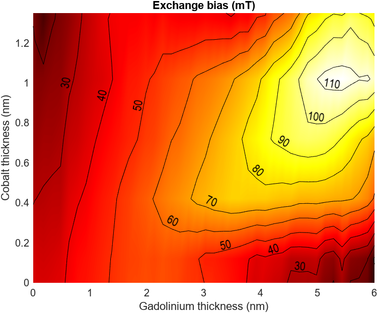
Optimizing \chCo/\chGd thicknesses - For optimizing the thicknesses of the \chGd and \chCo layers comprising the optically switchable layers, a sample similar to the one from the main text (Fig. 1a) was grown, but where the \chGd(5.5)/\chCo(1) layers were wedged. The \chGd thickness along the wedge varied from . The \chCo wedge was oriented at with respect to the \chGd wedge, such that each point on the sample corresponds to a unique combination of \chGd and \chCo thicknesses. This allowed us to map as a function of both \chGd and \chCo layer thickness. The measurement was carried out with a polar MOKE setup which measured the (-) hysteresis curves at a grid of positions. Subsequently, each hysteresis curve was used to extract the loop shift and hence estimate . The map is shown in Fig. S1. It can be seen that there is a clear peak visible at values of \chGd thickness and \chCo thickness. These were the thicknesses that were used in our final device
.
It may be seen as surprising that changing the \chGd thickness beyond a few nanometers still changes the magnetostatic properties, since the bulk Curie temperature of \chGd lies just below room temperature (). This indicates to us that indeed intermixing of \chCo sputtered on top \chGd plays a role, since in that case the antiferromagnetic coupling between the -\chCo and -\chGd atoms could give rise to a higher overall of the intermixed region.
Appendix S2 Spot size characterization
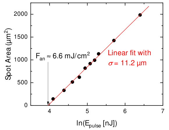
The spot size of the laser pulse can be determined from Kerr microscopy images after exciting the sample with various laser pulse energies (related to the measured power by the repetition rate ). If a Gaussian with standard deviation is assumed for the spatial distribution of the fluence
| (S1) |
then it is readily seen that the area above a certain threshold fluence depends linearly on the natural logarithm of the power , and the slope is equal to . An example of such a linear dependency is shown in Fig. S2 and gives a value of . This corresponds to a full width of at half maximum. For the data in Fig. S2, the Kerr images of the spots are taken at zero field after negative saturation. Note that it is important to keep the background field constant, because the spot grows or shrinks when the field changes. This in turn is because of the inhomogeneous distribution of switching fields as explained in Fig. 2 of the main text. If the spots are imaged at zero field, the switched area would correspond more or less with the annealing threshold , which for the data in Fig. S2 gives a value of around . This matches with the experimental data (compare for example with Fig. 4a of the main text).
Appendix S3 Implementation of the model
Our model of exchange bias reversal describes magnetization dynamics on two distinct timescales. The first part describes longitudinal switching of the ferro-/ferrimagnetic layers directly after the excitation by the laser. We run the simulation until the system temperature drops below the Néel temperature of the antiferromagnet. Then, in the second part, we simulate the stochastic setting process of the exchange bias through thermal excitations between distinct energy levels. For this, we take the polycrystalline nature of the antiferromagnet into account by estimating the grain size distribution and calculate the energy barrier for each particular grain size. The equations and parameters are worked out in more detail below.
S3.1 Part I: Longitudinal switching
The implementation of magnetization dynamics after laser pulse excitation closely follows Beens et al.[20]. Two temperature baths are considered: an electron () and a phonon bath (). The two baths exchange heat at a rate parameterized by . Heat enters the system via the electron bath by optical excitation from the laser pulse (fluence , pulse width ), and it relaxes predominantly through phonon heat dissipation to the substrate with a characteristic time scale . The temperature evolution then follows from a two-temperature model
| (S2) | |||
| (S3) |
where and are the electron and phonon heat capacities (respectively) and is the ambient temperature. It is assumed that every layer experiences the same volumetric fluence, a claim that is backed up by calculations of the absorption per layer in section S4.
As the temperature evolves, two processes are modeled that govern the magnetization dynamics. Firstly, spin angular momentum relaxation to the lattice occurs via Elliot-Yafet (EY) spin-flip scattering between an electron and a phonon with a spin-flip probability. Secondly, nearest-neighbor exchange scattering (EX) is taken into account, which describes scattering events between two electrons exchanging spin angular momentum. Because \chGd is classified as a ferromagnet with behavior corresponding to a spin quantum number of [33] (whereas for \chCo and \chMn the spin quantum number is best modeled as ), each of the spin levels must be simulated separately to account for all possible transitions. The occupation fraction of spin level for subsystem is , and the normalized magnetization is given by the weighted sum
| (S4) |
The spin levels have energies separated by an exchange splitting , i.e. the energy difference between level and . Each subsystem experiences a magnetic exchange interaction with its neighboring subsystems ( and ) and also from within its own subsystem (). Each is chosen in accordance with the Weiss model and the Curie temperatures associated with bulk systems of the different materials. If a closed-packed structure with texture is assumed, then each atom has 6 nearest-neighbors within the same layer and 3 nearest-neighbors in each adjacent layer. Altogether, the exchange splitting then becomes
| (S5) |
where the last term accounts for the Zeeman splitting (Bohr magneton and magnetic flux density ). The full rate equation as derived by Koopmans et al.[24] and Beens et al.[20] is given by
| (S6) |
where the full expressions of the terms on the right hand side are given in the supplementary materials of the respective references. The initial conditions for solving Eq. S6 follow from Boltzmann statistics and are obtained from solving
| (S7) |
The stack we simulate closely resembles the one used in the experiments and encompasses layers in total (see Fig. S3a). The antiferromagnet \chIrMn is modeled as a layered ferromagnet with negative interlayer exchange coupling , such that alternates from positive to negative between layers. Four atomic layers of \chIrMn are simulated in order to have a decent separation between the exchange bias interface and the edge of the system. Zeeman splitting is set to zero for all \chIrMn layers. The \chPt/\chCo multilayer in direct contact with the \chIrMn is modeled as a single ferromagnet (labeled \chPtCo) with three atomic layers, based on thickness with a typical atomic radius of . The \chPtCo system is coupled by a weaker direct exchange interaction to the \chCo layer below, which comprises five atomic layers. At the bottom, three \chGd layers are simulated whose magnetization will be induced by the coupling at the \chCo interface. Because this induced magnetization decays very rapidly away from the \chCo interface, adding more than three layers of \chGd does not significantly change the results.
Coercivity or anisotropy is not encapsulated in this model. To still account for the influence of on , it is assumed that a ferromagnetic layer prefers to orient itself along the field direction if the Zeeman splitting is greater than the exchange splitting for fully saturated layers with .
The simulation is run until drops below the Néel temperature of the \chIrMn layers. From the layered Weiss model and Eq. S7, this temperature amounts to (see Fig. S3b
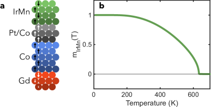
). At this point, magnetic order is established in the \chIrMn and the slower thermally assisted exchange bias setting process commences.
S3.2 Part II: Exchange bias setting
In this part of the simulation, the antiferromagnet is modeled by the parameter as a collection of columnar grains with distributed areas and thickness . The time and area dependence will henceforth be dropped for readability, but are always implicitly assumed. can be written as , where and are the proportions of grains with area that respectively have a positive or negative contribution to the perpendicular exchange bias. These proportions change over time under the influence of thermal excitations, with transition rates given by Eq. 1 in the main text. The rate equations for and can be summed into a single rate equation for given by
| (S8) |
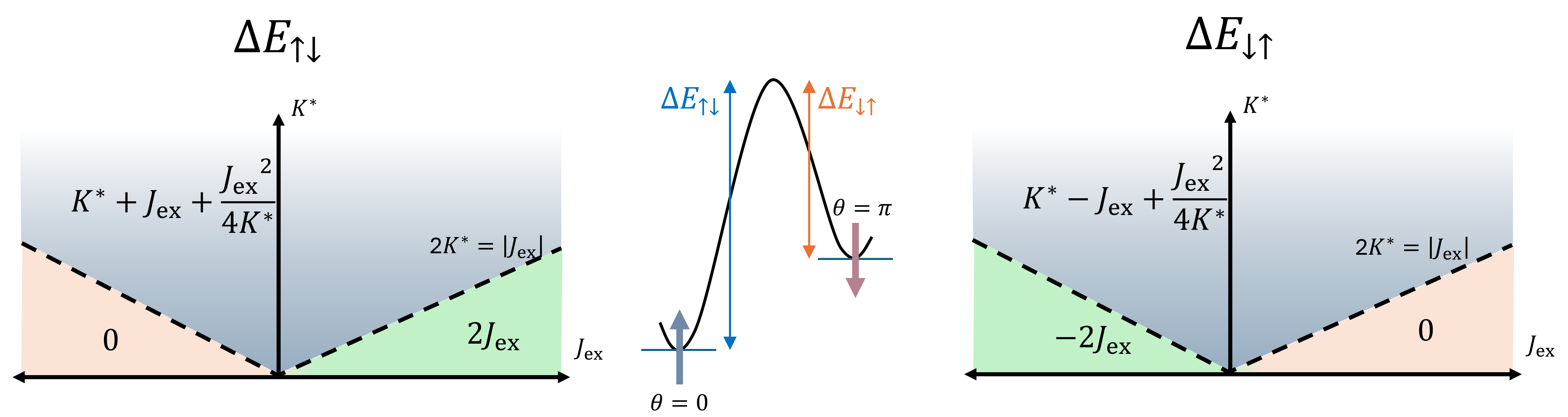
The energy barrier is calculated for a grain with area by taking into account the perpendicular antiferromagnetic anisotropy and the exchange coupling with the ferromagnet. If is the polar angle of the exchange bias direction, then an expression for the total energy per unit area becomes
| (S9) |
Figure S4 shows how the energy barrier changes for various combinations of and . The parameters and themselves depend on the state (temperature and magnetization) that the system is in. Heat is assumed to dissipate on the long timescales (i.e., long after and have equilibrated) according to a one-dimensional heat kernel (). At any time , we evaluate the temperature by[34]
| (S10) |
with such that and the peak temperature reached directly after equilibration of and . can be worked out by analytically solving Eq. S2 in the limit , and by solving . This gives
| (S11) | |||
| (S12) |
The temperature is fed back into the layered Weiss model (Eq. S7) at every simulation time step to work out the equilibrium magnetization at that particular temperature. The anisotropy and exchange coupling are also adapted accordingly, for which we assume
| (S13) |
where is the antiferromagnetic anisotropy at and is the exchange coupling for a fully saturated ferromagnet and antiferromagnet at .
The simulation (Eq. S8) is run over a time span of , after which the temperature has relaxed sufficiently close to room temperature and is no longer significantly changing. An example of such a simulation for is shown in Fig. S5a. This is then repeated for all possible grain areas , producing a distribution of switching fractions which we will call , an example of which is shown in Fig. S5b. Following Ref. 25, it is assumed that the grain areas are distributed according to a lognormal distribution with median area and standard deviation [25],
| (S14) |
also plotted in Fig. S5b. It must be taken into account that the smallest grains are not able to contribute to the exchange bias because they are superparamagnetic. The critical grain area that corresponds to this is given by
| (S15) |
Finally, taking the grain size distribution into account, the fraction of exchange bias remaining (relative to the maximum value for ) after the laser pulse excitation is given by
| (S16) |
The quantity on the left hand side is the output of the simulation and may then be further examined, e.g., as a function of fluence or magnetic field. Figure S5b
shows examples of the grain area distribution function and the fraction distribution function as simulated for a fluence of .
| [] | [] | [] | [] | [] | [] |
|---|---|---|---|---|---|
| [] | [] | [] | [] | [] | [] | [] | ||
|---|---|---|---|---|---|---|---|---|
| \chGd | 111From Ref. 24. | 777From Ref. 36 | 222From Ref. 20. | 222From Ref. 20. | 666, .[35] | - | - | |
| \chCo | 111From Ref. 24. | 111From Ref. 24. | 222From Ref. 20. | 222From Ref. 20. | 666, .[35] | 555Based on an interlayer exchange coupling strength that is of the \chPtCo intralayer exchange coupling. | - | |
| \chPtCo | 333Chosen the same as for \chCo. | 333Chosen the same as for \chCo. | 444The \chPtCo Curie temperature is chosen slightly below the bulk value to incorporate influences from size effects. | 333Chosen the same as for \chCo. | - | 555Based on an interlayer exchange coupling strength that is of the \chPtCo intralayer exchange coupling. | 888From experimental values: for atomic \chCo layers, assuming an fcc ordering with nearest neighbors of which are \chCo for each \chMn atom. Then: , . | |
| \chIrMn | 999Based on a material density of , an atomic mass of for \chMn, similar electronic properties (density of states and spin-flip probability) as for \chCo. Using parameters from the table and Eq. 19 from the supplementary of Ref. 24 gives the presented value. | 101010From Ref. 37. | 111111Néel temperature of bulk \chIr_0.2Mn_0.8. | 101010From Ref. 37. | - | - | 888From experimental values: for atomic \chCo layers, assuming an fcc ordering with nearest neighbors of which are \chCo for each \chMn atom. Then: , . |
respectively list the thermodynamic, micromagnetic and exchange bias setting parameters (constant or derived) as used in the two parts of the simulations.
S3.3 Linking between Part I and Part II
To summarize, Part I of the simulation models the longitudinal ultrafast deterministic AOS process with the M3TM, and Part II models the stochastic thermally-assisted setting process of the exchange bias following the Arrhenius law. The two parts are linked in the sense that we use the output of Part I as an input for Part II. Mainly, this comes down to the value of , which depends on the laser power and the heat capacities of the layers, and the value of , which is assumed to be with the sign depending on whether or not AOS has taken place. Moreover, since the simulation is forced to start only when the temperature has dropped below the Néel temperature of the \chIrMn, it may be assumed there is no significant disorder left within the grains themselves. We choose to set if , otherwise we assume no effect on the \chIrMn and we set to emulate the as-deposited fully aligned orientation of the grains.
Appendix S4 Skin-depth effects
As evident from section III.1 of the main text, skin-depth effects are relevant for determining the absorbed energy in each of the layers. This can be estimated by the transfer matrix method. We use a wavelength of and refractive indices for the different materials as given in table 4.
| Material [] | Refractive index |
|---|---|
| \chSi | |
| \chSiO2 | |
| \chTa | |
| \chPt | |
| \chCo | |
| \chGd | |
| \chIrMn |
The stack and substrate are identical to what is presented in section II of the main text. For an \chIrMn thickness of , the outcome of the calculated absorption is plotted in
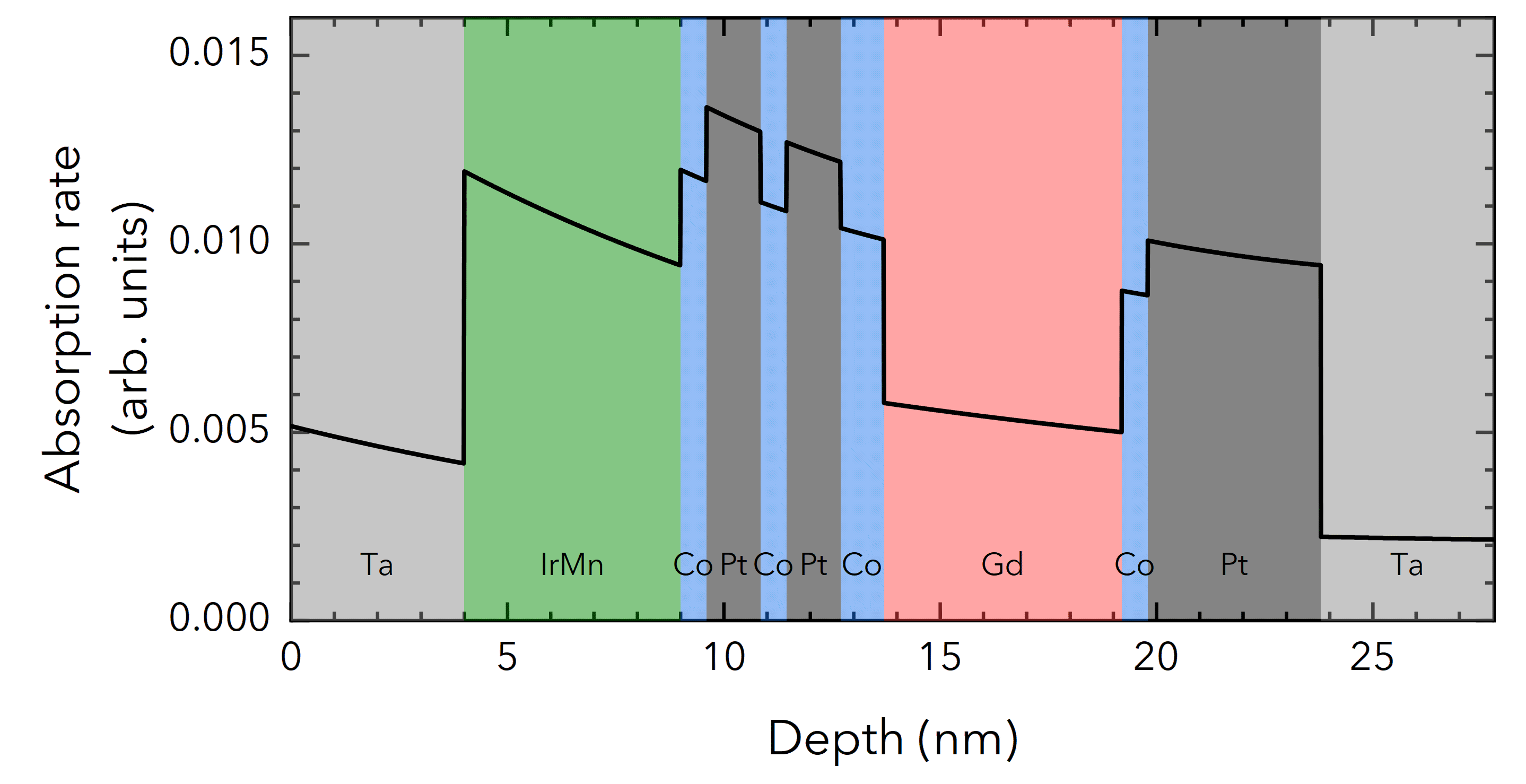
Fig. S6.
Relative to the bottom-most \chCo layer, the absorption per atomic layer for \chCo lies in the range , for \chPtCo in the range , for \chIrMn in the range and for \chGd in the range . As all these values are near unity, it was deemed valid to approximate the temperature as being uniform throughout the stack at all times in the simulation.
Appendix S5 Blocking temperature
Figure 3b of the main text claims a relation between and the blocking temperature . The measurement of was carried out with vibrating sample magnetometry (VSM) at various temperatures to locate the point at which the exchange bias vanishes. Because the stack from the main paper is engineered to have a very low magnetic moment, a different stack was measured with VSM to ensure a high enough signal. Five full film stacks were grown (with the same conditions as in the main text) consisting of \chTa(4)/\chPt(4)/\chCo(0.6)/[\chPt(1.25)/\chCo(0.6)]x9/\chIrMn()/\chTa(7), with . The data is shown in Fig. S7
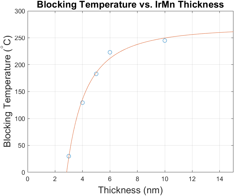
along with a fit according to a phenomenological power law with variable exponent given by [38]
| (S17) |
Here, is the theoretical limit of the blocking temperature for an infinitely thick antiferromagnetic layer and and respectively control the width and steepness of the trend. Fitted numerical values are given by , and .