Eliminating Surface Oxides of Superconducting Circuits with Noble Metal Encapsulation
Abstract
The lifetime of superconducting qubits is limited by dielectric loss, and a major source of dielectric loss is the native oxide present at the surface of the superconducting metal. Specifically, tantalum-based superconducting qubits have been demonstrated with record lifetimes, but a major source of loss is the presence of two-level systems (TLSs) in the surface tantalum oxide. Here, we demonstrate a strategy for avoiding oxide formation by encapsulating the tantalum with noble metals that do not form native oxide. By depositing a few nanometers of Au or AuPd alloy before breaking vacuum, we completely suppress tantalum oxide formation. Microwave loss measurements of superconducting resonators reveal that the noble metal is proximitized, with a superconducting gap over 80% of the bare tantalum at thicknesses where the oxide is fully suppressed. We find that losses in resonators fabricated by subtractive etching are dominated by oxides on the sidewalls, suggesting total surface encapsulation by additive fabrication as a promising strategy for eliminating surface oxide TLS loss in superconducting qubits.
Superconducting qubits are the basis of many large scale quantum processors, enabling demonstrations of quantum error correction [1, 2, 3], quantum many body physics [4, 5, 6, 7], and quantum simulation [8, 9, 10]. Despite this progress, single qubit coherence remains a major limiting factor in building scalable processors based on superconducting qubits. Single qubit coherence is limited by dielectric loss, particularly at surfaces and interfaces [11, 12, 13, 14]. Tantalum-based superconducting qubits have recently been discovered to enable record lifetimes and coherence times [15, 16, 17]. Losses in state-of-the-art tantalum devices are dominated by TLSs in surface oxides and the bulk substrate [18, 19]. Avoiding the formation of surface oxides would eliminate this loss channel, and recent studies have demonstrated that encapsulation with other materials can mitigate losses associated with surface oxides of niobium [20, 21], pointing to a potential strategy for avoiding surface losses in tantalum (Ta).
Here we encapsulate Ta superconducting resonators by depositing a noble metal (gold or gold-palladium) after the Ta deposition, before breaking vacuum. We characterize the film using x-ray photoelectron spectroscopy (XPS), scanning transmission electron microscopy (STEM), electron energy loss spectroscopy (EELS), and energy-dispersive x-ray spectroscopy (EDX) to show that the tantalum oxide is completely suppressed with only a few nanometers of noble metal encapsulation. The noble metal encapsulation layer is a normal (non-superconducting) metal, so it may contribute to additional loss if the normal metal is not fully proximitized by the underlying superconducting film [22, 23, 24, 25]. We fabricate resonators with these encapsulated films, and perform microwave measurements to confirm the proximitization of the noble metal layer and to determine the effective superconducting gap of the heterostructure, which varies with encapsulation thicknesses. By fitting the dependence of the effective gap on encapsulation thickness with numerical solutions of the Usadel equations [26], we estimate an interface transparency and find that it is consistent with a high quality, Ohmic contact. By comparing materials characterization with microwave device measurements, we find a wide range of encapsulation thicknesses that suppress the surface oxide while maintaining a high quality factor at base temperatures, from 3 nm to 26 nm. These results point to a promising strategy for eliminating surface oxide loss via total encapsulation and additive nanofabrication.
We deposit gold (Au) or gold palladium alloy (AuPd) on top of 200 nm thick -Ta films grown on 550 m thick c-plane sapphire substrates with dc magnetron sputtering [27, 28, 29, 30, 31]. The Au (AuPd) encapsulation layer is deposited in situ right after the Ta film growth inside an ultra high vacuum chamber (with base pressure value of Torr), avoiding the growth of native oxide, as verified by STEM [Figs. 1(a,b)].
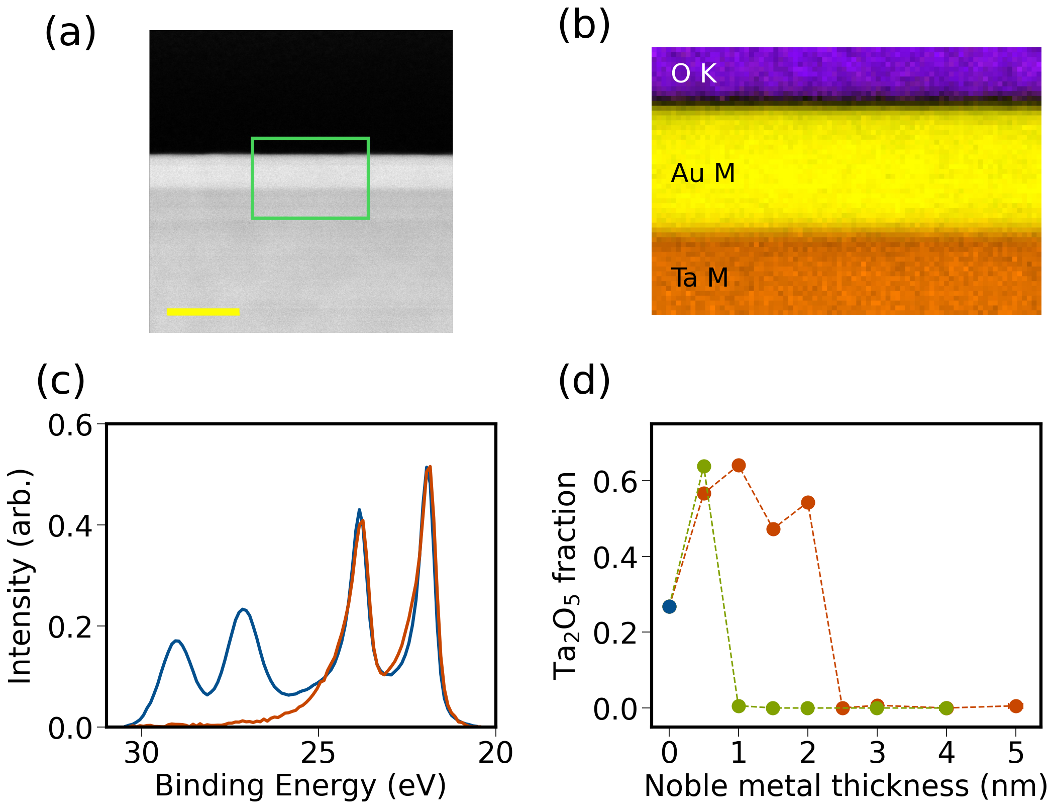
In order to quantify the degree of surface oxidation, we use XPS to measure the atomic percentage of tantalum pentoxide (Ta2O5) in the Ta4f spectrum [Figs. 1(c,d)]. The Ta4f spectrum consists of 2 sets of doublet peaks, metallic Ta at 22 eV and 24 eV and Ta2O5 at 27 eV and 29 eV [32, 19] [Fig. 1(c)]. The Ta2O5 peaks are not present in the binding energy spectrum of Au-encapsulated Ta, demonstrating that the amorphous surface oxides of Ta have been suppressed.
We systematically investigate the encapsulation conditions needed to fully suppress the tantalum oxide by measuring Ta4f XPS spectra for various thicknesses of Au or AuPd encapsulation layers and extracting the intensity of the Ta2O5 peaks. Note that for very thin encapsulation layers, we report an effective thickness based on deposition rates, see [27] for more details. We obtain higher Ta2O5 intensity with nominal Au (AuPd) thickness less than 2.5 (1) nm, which we hypothesize is caused by an oxidation catalysis effect from small Au (AuPd) islands [27, 33, 34]. However, we find that 2.5 (1) nm of encapsulating Au (AuPd) is enough to fully suppress the tantalum oxide [Fig. 1(d)], which indicates a material-dependent critical thickness at which the encapsulation film completely covers the Ta surface and forms an oxygen diffusion barrier.
We measure the degree of proximitization of the noble metal encapsulation by fabricating coplanar waveguide (CPW) quarter-wave resonators on various encapsulated Ta films with designs that were used in our prior work [18]. The losses associated with TLSs and quasiparticles (QPs) can be characterized by measuring the resonance frequency as a function of temperature, or alternatively by measuring the internal quality factor as a function of intracavity photon number and temperature [18, 35]. From these measurements, the effective superconducting gap energy can be extracted [18, 27].
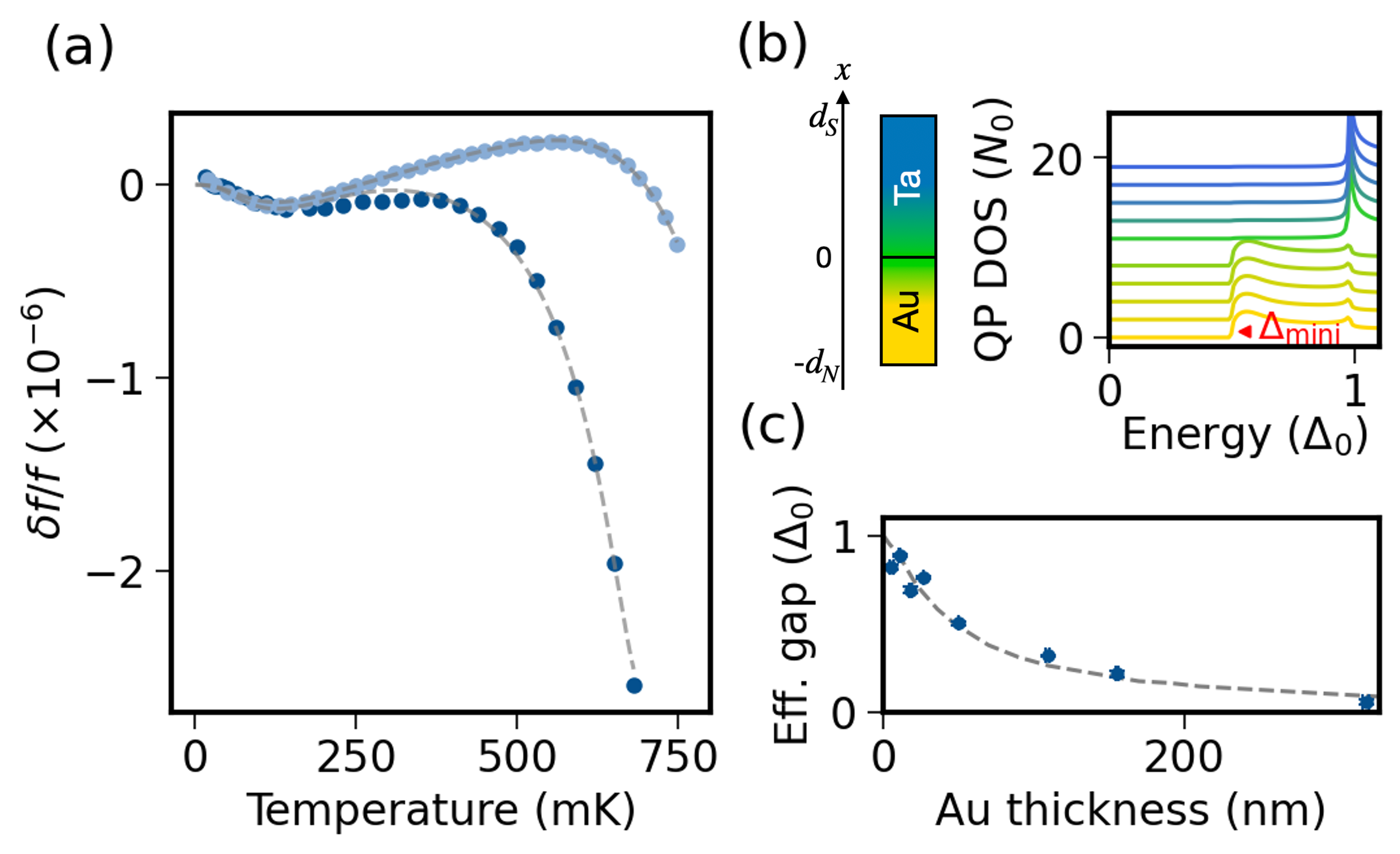
As a representative example, the frequency shift of resonators with 5 nm and 50 nm Au encapsulation layers that are otherwise identical is markedly different in the high temperature regime [Fig. 2(a)]. In the low temperature regime, the non-monotonic dependence of frequency on temperature is dominated by TLSs [36, 18], and the two resonators exhibit similar behavior. At higher temperatures, the more rapid change in frequency with temperature is caused by thermal quasiparticles [35, 37]. With a thicker encapsulating layer we observe a larger change in the frequency shift at high temperature, indicating a larger population of thermal quasiparticles [Fig. 2(a)]. These effects can be parameterized by a reduction in the effective superconducting gap energy of the film. This softening of the gap can be understood through the superconducting proximity effect [22, 23, 24, 25].
We quantitatively investigate the superconducting nature of encapsulated Ta films by extracting the effective gap of films undergoing additional iterative sputtering of Au to vary the encapsulation layer thickness from 5 to 323 nm [Fig. 2(c)]. We observe a decrease in the effective gap in our devices as the encapsulation thickness increases. These results can be explained by distortions in the quasiparticle density of states (DOS) across the superconductor-normal metal interface caused by the proximity effect. Our measurements are particularly sensitive to higher populations of thermal quasiparticles induced by the opening of a superconducting energy gap smaller than the bulk Ta gap () in the normal metal layer denoted as the minigap, [Fig. 2(b)][22, 23]. Here, the microwave resonator measurements are dominated by changes in the surface impedance of the film, and are thus most sensitive to the properties of the normal metal layer at the surface.
To understand the evolution of minigap size with increasing thicknesses of encapsulating Au, we fit our data to numerically calculated minigaps using the Usadel equations [Fig. 2(c)][38, 39, 26, 27, 40, 41, 42]. The only free fit parameter is the electron interface transparency, which we fit to a value of (see [27] for details on error estimations). This high interface transparency is consistent with the suppression of tantalum oxide and the formation of an Ohmic contact, and it is comparable with other reported transparency values of superconductor-normal metal interfaces grown via in situ sputtering [23, 43, 38].
For Au encapsulation thicknesses of around 3 nm where the tantalum oxide is completely suppressed [Fig. 1(d)], the effective gap energy is still greater than 80% of the bulk Ta gap. We observe an ideal range of encapsulation thicknesses from 3 to 26 nm over which encapsulated resonators maintain a high quality factor () at base temperatures and high powers. These results indicate that encapsulated Ta films are a viable material platform for fabricating superconducting circuits with minimal reduction in the effective gap.
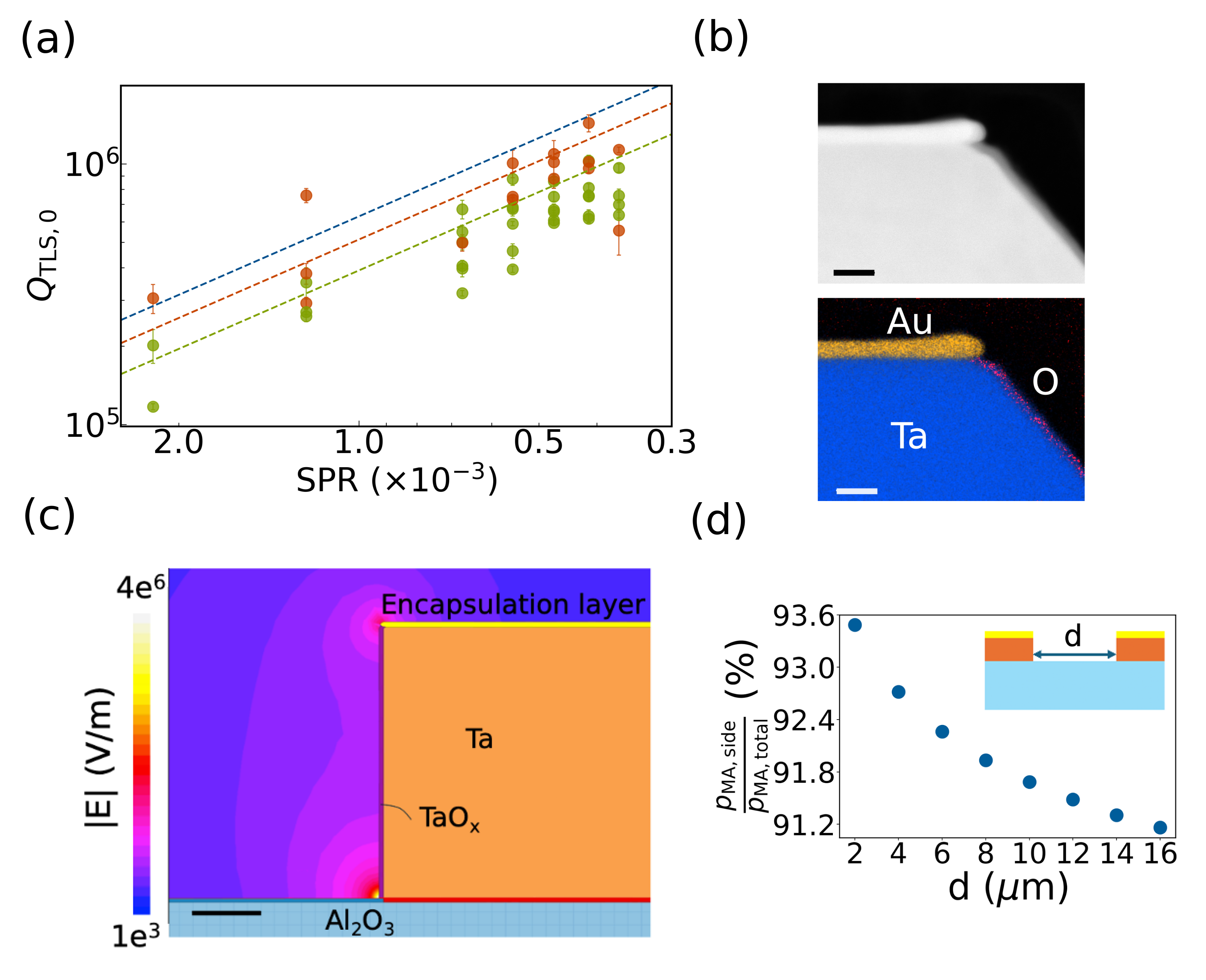
To characterize the surface and interface losses of encapsulated resonators, we vary their geometry to change the surface participation ratio (SPR) of the electric field energy [44, 18]. By measuring the temperature-dependent frequency shift, as well as the dependence of internal quality factor on temperature and intracavity photon number, we can also extract the linear absorption due to TLSs, denoted as , see [18, 27] for details. This extracted parameter captures the contribution of TLSs to dielectric loss. We fit a linear relationship between extracted values and SPR, taking the fitted slope to be the surface TLS dielectric loss tangent [Fig. 3(a), Table 1] [18, 27]. Fitted loss tangents for each film type are also plotted along with loss tangent values for bare Ta devices obtained in our previous work as comparison [18].
| Film | ||
|---|---|---|
| Bare Ta | [18] | |
| Au encapsulation | [This work] | |
| AuPd encapsulation | [This work] | |
Despite the suppression of surface oxides, we do not observe an improvement in the surface TLS loss, and we observe slightly higher surface loss tangents with encapsulated films compared to bare Ta devices. Because our resonators are patterned by a subtractive etch process, the fabrication-exposed sidewalls are not encapsulated and thus grow surface oxide, which can be observed in TEM images [Fig. 3(b)]. To determine the contribution of the sidewall oxide on device performance, we perform dc finite element electric field simulations (Ansys Maxwell) on the cross section of encapsulated devices to determine the contribution of the sidewall oxide to the electric field energy’s surface participation. We assume a 3 nm thick oxide layer with dielectric constant 10 on the sidewall and a 4 nm thick encapsulation layer. These two layers make up the the modeled metal-air interface in our devices. We denote the total electric field energy participation in both of these two layers as , and the electric field energy participation in the sidewall oxide as . The sidewall oxide dominates the total participation ratio, accounting for more than 90% of electric field energy participation along the metal-air interfaces across all device geometries [Fig. 3(d)]. The large participation ratio of the sidewall oxide arises from the 2D geometry of the device, in which the field resides in the gap between metal structures and is concentrated at the corners [Fig. 3(c)].
Beyond the sidewall oxide, the slightly higher measured surface loss tangents of encapsulated devices may arise from increased sidewall roughness. The multilayer structure requires multiple etching steps in the resonator fabrication process, and the additional etching step causes rougher sidewall profiles compared to bare Ta devices [27]. Rougher sidewalls have higher surface area and can concentrate the electric field, and thus increase the surface participation ratio beyond the simulated value, leading to a higher fitted surface loss tangent.
Here we have demonstrated complete suppression of the native surface oxide of Ta using noble metal encapsulation, and we find that these films remain superconducting because of proximitization of the encapsulation layer by the underlying Ta. These encapsulated resonators exhibit performance that is similar to state-of-the-art Ta circuits at mK temperatures. Our ongoing work includes developing fabrication strategies that can achieve total Ta encapsulation to avoid the formation of oxides on the device sidewalls, for example by additive fabrication [45]. Beyond improving the performance of superconducting qubits, our strategy for superconducting gap engineering via noble metal encapsulation may have applications in on-chip filters for quasiparticle trapping [46] and multi-channel kinetic inductance detectors [47, 48].
Acknowledgements.
Acknowledgements.— We thank Basil Smitham, Kevin Crowley, and Lev Krayzman for helpful discussions. This work was primarily supported by the U.S. Department of Energy, Office of Science, National Quantum Information Science Research Centers, Co-design Center for Quantum Advantage (C2QA) under Contract No. DE-SC0012704. Materials growth and analysis was partially supported by the National Science Foundation (RAISE DMR-1839199). The authors acknowledge the use of Princeton’s Imaging and Analysis Center (IAC), which is partially supported by the Princeton Center for Complex Materials (PCCM), a National Science Foundation Materials Research Science and Engineering Center (MRSEC; DMR-2011750), as well as the Princeton Micro/Nano Fabrication Laboratory. We also acknowledge MIT Lincoln Labs for supplying a traveling wave parametric amplifier.Princeton University Professor Andrew Houck is also a consultant for Quantum Circuits Incorporated (QCI). Due to his income from QCI, Princeton University has a management plan in place to mitigate a potential conflict of interest that could affect the design, conduct and reporting of this research.
References
- Sivak et al. [2023] V. V. Sivak, A. Eickbusch, B. Royer, S. Singh, I. Tsioutsios, S. Ganjam, A. Miano, B. L. Brock, A. Z. Ding, L. Frunzio, S. M. Girvin, R. J. Schoelkopf, and M. H. Devoret, Real-time quantum error correction beyond break-even, Nature 616, 50 (2023).
- Acharya et al. [2023] R. Acharya et al., Suppressing quantum errors by scaling a surface code logical qubit, Nature 614, 676 (2023).
- Koottandavida et al. [2024] A. Koottandavida et al., Erasure detection of a dual-rail qubit encoded in a double-post superconducting cavity, Phys. Rev. Lett. 132, 180601 (2024).
- Kollár et al. [2019] A. J. Kollár, M. Fitzpatrick, and A. A. Houck, Hyperbolic lattices in circuit quantum electrodynamics, Nature 571, 45 (2019).
- Mi et al. [2022] X. Mi et al., Time-crystalline eigenstate order on a quantum processor, Nature 601, 531 (2022).
- Andersen et al. [2023] T. I. Andersen et al., Non-abelian braiding of graph vertices in a superconducting processor, Nature 618, 264 (2023).
- Andersen et al. [2024] T. I. Andersen et al., Thermalization and criticality on an analog-digital quantum simulator (2024), arXiv:2405.17385 [quant-ph] .
- Karamlou et al. [2022] A. H. Karamlou et al., Quantum transport and localization in 1d and 2d tight-binding lattices, npj Quantum Information 8, 35 (2022).
- Martinez et al. [2023] J. G. C. Martinez, C. S. Chiu, B. M. Smitham, and A. A. Houck, Flat-band localization and interaction-induced delocalization of photons, Science Advances 9, eadj7195 (2023), https://www.science.org/doi/pdf/10.1126/sciadv.adj7195 .
- Karamlou et al. [2024] A. H. Karamlou et al., Probing entanglement in a 2d hard-core bose–hubbard lattice, Nature 629, 561 (2024).
- Read et al. [2023] A. P. Read, B. J. Chapman, C. U. Lei, J. C. Curtis, S. Ganjam, L. Krayzman, L. Frunzio, and R. J. Schoelkopf, Precision measurement of the microwave dielectric loss of sapphire in the quantum regime with parts-per-billion sensitivity, Phys. Rev. Appl. 19, 034064 (2023).
- de Leon et al. [2021] N. P. de Leon, K. M. Itoh, D. Kim, K. K. Mehta, T. E. Northup, H. Paik, B. S. Palmer, N. Samarth, S. Sangtawesin, and D. W. Steuerman, Materials challenges and opportunities for quantum computing hardware, Science 372, eabb2823 (2021).
- Krupka et al. [1999a] J. Krupka, K. Derzakowski, M. Tobar, J. Hartnett, and R. G. Geyer, Complex permittivity of some ultralow loss dielectric crystals at cryogenic temperatures, Meas. Sci. Technol. 10, 387 (1999a).
- Krupka et al. [1999b] J. Krupka, K. Derzakowski, A. Abramowicz, M. Tobar, and R. Geyer, Use of whispering-gallery modes for complex permittivity determinations of ultra-low-loss dielectric materials, IEEE Trans. Microw. Theory Tech. 47, 752 (1999b).
- Place et al. [2021] A. P. M. Place et al., New material platform for superconducting transmon qubits with coherence times exceeding 0.3 milliseconds, Nat. Commun. 12, 1779 (2021).
- Wang et al. [2022] C. Wang et al., Towards practical quantum computers: transmon qubit with a lifetime approaching 0.5 milliseconds, npj Quantum Information 8, 3 (2022).
- Ganjam et al. [2024] S. Ganjam, Y. Wang, Y. Lu, A. Banerjee, C. U. Lei, L. Krayzman, K. Kisslinger, C. Zhou, R. Li, Y. Jia, M. Liu, L. Frunzio, and R. J. Schoelkopf, Surpassing millisecond coherence in on chip superconducting quantum memories by optimizing materials and circuit design, Nature Communications 15, 3687 (2024).
- Crowley et al. [2023] K. D. Crowley et al., Disentangling losses in tantalum superconducting circuits, Phys. Rev. X 13, 041005 (2023).
- McLellan et al. [2023] R. A. McLellan et al., Chemical profiles of the oxides on tantalum in state of the art superconducting circuits, Advanced Science 10, 2300921 (2023), https://onlinelibrary.wiley.com/doi/pdf/10.1002/advs.202300921 .
- Bal et al. [2024] M. Bal et al., Systematic improvements in transmon qubit coherence enabled by niobium surface encapsulation, npj Quantum Information 10, 43 (2024).
- de Ory et al. [2024] M. C. de Ory, D. Rodriguez, M. T. Magaz, V. Rollano, D. Granados, and A. Gomez, Low loss hybrid nb/au superconducting resonators for quantum circuit applications (2024), arXiv:2401.14764 .
- Belzig et al. [1996] W. Belzig, C. Bruder, and G. Schön, Local density of states in a dirty normal metal connected to a superconductor, Phys. Rev. B 54, 9443 (1996).
- Barends et al. [2009] R. Barends, W. K. Daalman, A. Endo, S. Zhu, T. Zijlstra, and T. M. Klapwijk, Frequency and quality factor of NbTiN/Au bilayer superconducting resonators, AIP Conference Proceedings 1185, 152 (2009), https://pubs.aip.org/aip/acp/article-pdf/1185/1/152/12248182/152_1_online.pdf .
- Gurevich and Kubo [2017] A. Gurevich and T. Kubo, Surface impedance and optimum surface resistance of a superconductor with an imperfect surface, Phys. Rev. B 96, 184515 (2017).
- Ustavshchikov et al. [2019] S. S. Ustavshchikov, A. Y. Aladyshkin, V. V. Kurin, V. A. Markelov, A. I. El’kina, A. M. Klushin, P. A. Yunin, V. V. Rogov, and D. Y. Vodolazov, Microwave impedance of thin-film superconductor–normal metal hybrid structures with a high conductivity ratio, Physics of the Solid State 61, 1675 (2019).
- Usadel [1970] K. D. Usadel, Generalized diffusion equation for superconducting alloys, Phys. Rev. Lett. 25, 507 (1970).
- [27] See supplemental material at [url will be inserted by publisher] for details on film growth, device fabrication, film characterization, and theoretical models.
- Face and Prober [1987] D. W. Face and D. E. Prober, Nucleation of body-centered-cubic tantalum films with a thin niobium underlayer, Journal of Vacuum Science & Technology A: Vacuum, Surfaces, and Films 5, 3408–3411 (1987).
- Gladczuk et al. [2004] L. Gladczuk, A. Patel, C. Paur, and M. Sosnowski, Tantalum films for protective coatings of steel, Thin Solid Films 467, 150 (2004).
- Nakagomi and Kokubun [2012] S. Nakagomi and Y. Kokubun, Crystal orientation of beta-ga2o3 thin films formed on c-plane and a-plane sapphire substrate, Journal of Crystal Growth 349, 12 (2012).
- Mukherjee et al. [2012] D. Mukherjee, P. Mukherjee, H. Srikanth, and S. Witanachchi, Carrier-mediated interaction of magnetic moments in oxygen vacancy–controlled epitaxial Mn-doped ZnO thin films, Journal of Applied Physics 111, 07C318 (2012), https://pubs.aip.org/aip/jap/article-pdf/doi/10.1063/1.3679067/15087033/07c318_1_online.pdf .
- Moulder et al. [1992] J. F. Moulder, W. F. Stickle, P. E. Sobol, and K. D. Bomben, Handbook of X-ray Photoelectron Spectroscopy: A Reference Book of Standard Spectra for Identification and Interpretation of XPS Data (Physical Electronics Division, Perkin-Elmer Corporation, Eden Prairie, MN USA., 1992).
- Hu et al. [2021] C. Hu, Z. Chen, C. Wei, X. Wan, W. Li, and Q. Lin, Au nanoparticles supported on iron-based oxides for soot oxidation: Physicochemical properties before and after the reaction, ACS Omega 6, 11510 (2021).
- Yang et al. [2022] H. Yang et al., Enhancing co oxidation activity via tuning a charge transfer between gold nanoparticles and supports, The Journal of Physical Chemistry C 126, 4836 (2022).
- Gao [2008] J. Gao, The Physics of Superconducting Microwave Resonators, Ph.D. thesis, California Institute of Technology (2008).
- Quintana et al. [2014] C. M. Quintana et al., Characterization and reduction of microfabrication-induced decoherence in superconducting quantum circuits, Appl. Phys. Lett. 105, 062601 (2014).
- Grünhaupt [2018] L. Grünhaupt, Loss mechanisms and quasiparticle dynamics in superconducting microwave resonators made of thin-film granular aluminum, Phys. Rev. Lett. 121, 10.1103/PhysRevLett.121.117001 (2018).
- Martinis et al. [2000] J. M. Martinis, G. Hilton, K. Irwin, and D. Wollman, Calculation of tc in a normal-superconductor bilayer using the microscopic-based usadel theory, Nuclear Instruments and Methods in Physics Research Section A: Accelerators, Spectrometers, Detectors and Associated Equipment 444, 23 (2000).
- De Gennes [1964] P. G. De Gennes, Boundary effects in superconductors, Rev. Mod. Phys. 36, 225 (1964).
- Belzig et al. [1999] W. Belzig, F. K. Wilhelm, C. Bruder, G. Schön, and A. D. Zaikin, Quasiclassical green’s function approach to mesoscopic superconductivity, Superlattices and Microstructures 25, 1251 (1999).
- Ashcroft and Mermin [2011] N. Ashcroft and N. Mermin, Solid State Physics (Cengage Learning, 2011).
- Bobrov et al. [2015] N. Bobrov, L. Rybal’chenko, V. Fisun, and I. Yanson, Point-contact electron-phonon interaction function in tantalum, arXiv preprint arXiv:1512.01800 (2015).
- Hennings-Yeomans et al. [2020] R. Hennings-Yeomans et al., Controlling Tc of iridium films using the proximity effect, Journal of Applied Physics 128, 154501 (2020), https://pubs.aip.org/aip/jap/article-pdf/doi/10.1063/5.0018564/14112105/154501_1_online.pdf .
- Wang et al. [2015] C. Wang, C. Axline, Y. Y. Gao, T. Brecht, Y. Chu, L. Frunzio, M. H. Devoret, and R. J. Schoelkopf, Surface participation and dielectric loss in superconducting qubits, Appl. Phys. Lett. 107, 162601 (2015).
- Tsioutsios et al. [2020] I. Tsioutsios, K. Serniak, S. Diamond, V. V. Sivak, Z. Wang, S. Shankar, L. Frunzio, R. J. Schoelkopf, and M. H. Devoret, Free-standing silicon shadow masks for transmon qubit fabrication, AIP Advances 10, 065120 (2020), https://pubs.aip.org/aip/adv/article-pdf/doi/10.1063/1.5138953/18296633/065120_1_1.5138953.pdf .
- McEwen et al. [2024] M. McEwen et al., Resisting high-energy impact events through gap engineering in superconducting qubit arrays (2024), arXiv:2402.15644 [quant-ph] .
- Vissers et al. [2013] M. R. Vissers, J. Gao, M. Sandberg, S. M. Duff, D. S. Wisbey, K. D. Irwin, and D. P. Pappas, Proximity-coupled ti/tin multilayers for use in kinetic inductance detectors, Applied Physics Letters 102, 10.1063/1.4804286 (2013).
- Hu et al. [2020] J. Hu, M. Salatino, A. Traini, C. Chaumont, F. Boussaha, C. Goupil, and M. Piat, Proximity-coupled al/au bilayer kinetic inductance detectors, Journal of Low Temperature Physics 199, 355 (2020).