SI.pdf
Stacking-Dependent Van Hove Singularity Shifts in Three-Dimensional Charge Density Waves of Kagome Metals V3Sb5 ( = K, Rb, Cs)
Abstract
Vanadium-based kagomé systems V3Sb5 ( = K, Rb, Cs) have emerged as paradigmatic examples exhibiting unconventional charge density waves (CDWs) and superconductivity linked to van Hove singularities (VHSs). Despite extensive studies, the three-dimensional (3D) nature of CDW states in these systems remains elusive. This study employs first-principles density functional theory and a tight-binding model to investigate the stacking-dependent electronic structures of 3D CDWs in V3Sb5, emphasizing the significant role of interlayer coupling in behaviors of the VHSs associated with diverse 3D CDW orders. We develop a minimal 3D tight-binding model and present a detailed analysis of band structures and density of states for various 3D CDW stacking configurations, including those with and without a -phase shift stacking of the inverse star of David, as well as alternating stacking of the inverse star of David and the star of David. We find that VHSs exist below the Fermi level even in 3D CDWs without -phase shift stackings, and that these VHSs shift downward in the -phase shift stacking CDW structure, stabilizing the -shifted inverse star of David distortions in alternating vanadium layers as the ground state 3D CDW order of V3Sb5. Our work provides the electronic origin of 3D CDW orders, paving the way for a deeper understanding of CDWs and superconductivity in V3Sb5 kagomé metals.
1 Introduction
A kagomé lattice refers to a two-dimensional network of corner-sharing triangles. It offers a fertile ground for studying the intricate interplay between frustrated geometry, topology, and electronic correlations. The electronic energy band structure of a kagomé lattice generically features a flat band, VHSs, and a pair of Dirac points. Depending on the electron filling, various captivating quantum phenomena have been explored, such as quantum topology and geometry [1, 2, 3], superconductivity [4, 5, 6, 7], and quantum magnets [8, 9, 10, 11, 12]. The kagomé lattice in stable materials has been a target of rigorous research efforts, resulting in many experimentally verified materials. Notable examples include FeSn [13], Fe3Sn2 [14], and CoSn [15], which illustrates physics originating from flatbands. More recently, kagomé metals such as V3Sb5 [16, 17, 18] and Ti3Bi5 [19, 20, 21] for = K, Rb, or Cs and V6Sn6 [22, 23, 24] ( = rare earth), and FeGe [25, 26, 27], have been under intensive investigation to study phenomena associated with the VHSs.
The vanadium-based kagomé metal V3Sb5 ( = Cs, K, and Rb) has become a prototypical system within the family of kagomé metals. It hosts multiple VHSs near Fermi level that exhibit rich properties [28, 29, 30, 31], and these VHSs have been found to play a significant role in driving unconventional phenomena [32, 33]. Notably, the onset of an anomalous Hall effect [34, 35] occurs concurrently with the CDW phase transition below K [17, 36, 37, 38]. The presence of Hall conductivity signals the time-reversal symmetry breaking [39, 40, 41, 42], which is further evidenced by various experiment methods [43, 44, 45]. Moreover, six-fold rotation symmetry breaking at is observed [46, 47, 48, 49, 50, 51, 52, 53, 54], followed by additional rotational symmetry breaking at lower temperatures [55, 56], which is assigned as electronic nematicity [45, 54, 55]. Upon further cooling, superconductivity emerges with a critical temperature c 0.9–2.5 K [17, 36, 37] and the superconductivity is found to compete with CDW [52, 57, 58, 59]
| KV3Sb5 | -0.010 | 0.330 | 0.045 | 0.040 | 0.048 | -0.009 | 0.018 | -0.006 |
|---|---|---|---|---|---|---|---|---|
| RbV3Sb5 | 0.020 | 0.340 | 0.036 | 0.050 | 0.048 | -0.007 | 0.022 | -0.004 |
| CsV3Sb5 | 0.080 | 0.365 | 0.010 | 0.060 | 0.048 | -0.006 | 0.030 | -0.004 |
| CsV3Sb5 (SD+ISD) | 0.100 | 0.380 | 0.025 | 0.060 | 0.048 | -0.006 | 0.030 | -0.004 |
Despite extensive studies [42, 60, 61, 62, 63, 64, 65, 66], the underlying mechanism of the CDW state, particularly its 3D nature, is not fully understood. It has been well established that the in-plane CDW pattern is either star of David (SD) or inverse star of David (ISD) type distortion in the single vanadium kagomé layer [29, 60, 67]. The CDW state in V3Sb5 exhibits a 3D nature with a modulation along the (out-of-plane) axis. Moreover, CsV3Sb5 is also found to exhibit a CDW state with a periodicity under certain conditions [67, 68, 69, 70], distinguishing it from KV3Sb5 and RbV3Sb5. The energetics of VHSs responsible for the emergence of 3D CDW can provide insight into these phenomena, as the presence of VHSs near the Fermi level is known to contribute to various phenomena, such as superconductivity [71, 72, 73], magnetism [74, 75], and nematicity [76]. Nevertheless, the origin of such intricate CDW order in V3Sb5 remains a topic of ongoing research.
In this paper, we use first-principles density functional theory (DFT) and a tight-binding (TB) model to investigate the influence of interlayer interactions on the electronic structure of V3Sb5 ( = K, Rb, Cs) kagomé systems, with a particular emphasis on changes in the VHS near the Fermi level depending on various 3D CDW stacking configurations. We develop a minimal 3D TB model that effectively captures interlayer interactions. This model faithfully reproduces the DFT bands and density of states for all three V3Sb5 compounds. Our investigation reveals the critical role of interlayer interactions among vanadium layers in describing the diverging electronic density of states near the Fermi level, which influences the ground state 3D CDW order. Based on our comprehensive calculations, we demonstrate that in 3D CDW structures without a -phase shift, the VHS is close to the Fermi level. However, in the ISD structure with lateral -phase shift stacking, the VHS moves sufficiently below the Fermi level, stabilizing this configuration as the ground state 3D CDW order. Our findings contribute to the understanding of the origin of 3D CDW orders observed in kagomé metals.
2 Methods
2.1 DFT methods
To investigate the electronic structures of V3Sb5 ( = K, Rb, SC), we performed first-principles calculations based on density functional theory (DFT) as implemented in the Vienna ab initio simulation package (VASP) [77, 78, 79, 80]. We used Perdew-Burke-Ernzerhof (PBE) [81] within the generalized gradient approximation (GGA) to describe the exchange and correlation functionals. We used projector augmented wave (PAW) pseudopotentials [82] and plane basis set with an energy cutoff of 300 eV. We applied the zero-damping DFT-D3 [83] van der Waals correction throughout our calculations. Brillouin zone integration was performed using the -centered sampling with -mesh for the unit cell and -mesh for the unit cell. The geometry of the structures was optimised until all forces are below 0.01 eV/Å. We used the Wannier90 package [84] to generate maximally localized Wannier functions (MLWFs) [85, 86, 87], enabling us to obtain the Fermi surface (FS). Subsequently, we extracted constant energy contours from the FS using the FermiSurfer tool [88].
2.2 Tight-binding model
We construct a 24-band tight-binding model that describes the orbitals (in local coordinates) of the vanadium kagomé layers within a supercell. The -orbital tight-binding model gives rise to the irreducible representation for the VHS state at the M point near the Fermi level in the pristine structure (see also Ref. [31]). The amplitude of the hopping parameters was determined so that the DFT bands were reproduced. We introduce a twelve-component spinor in the unit cell of the vanadium kagomé layer and write the tight-binding Hamiltonian as
The spinor is composed of three different sublattices and , where
for . The refers to the sublattice in the -th site within the supercell, as shown in Fig. 1 (see also Fig. S1 in the Supplemental Information). Our minimal TB Hamiltonian can be grouped into
| (1) | ||||
Here, and are the nearest-neighbor (NN) and next-nearest-neighbor (NNN) hopping matrices within the 2D kagomé layer. and are the NN hopping matrices that describe the SD and ISD type distortions [Figs. 1(d) and 1(e)], respectively. accounts for the interlayer hoppings between out-of-plane vanadium sites [Fig. 1(f)], specified by the level of nearest neighbors as
| (2) | ||||
The detailed forms of these matrices are given in the Supplemental Information333See the detailed forms of matrices of the tight-binding Hamiltonian. Previous tight-binding models have been developed to accurately describe multiple VHSs near the Fermi energy [89, 90] and band topology [91], including the Sb orbital. Our model differs from these models in that it excludes the Sb orbital and focuses on generically describing a single VHS near the Fermi level originating from the plane that is sensitive to the 3D CDW formation. This approach focuses on the instability in the supercell structure to explore the instability in the 3D stacking configurations of the CDW phases.
3 Results and Discussion
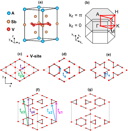
Let us first briefly introduce the atomic structure of V3Sb5 in the pristine and CDW phases. The pristine phase of V3Sb5 has a layered hexagonal structure (space group , No. 191). This structure features specific atomic positions and stacking configurations, shown in Fig. 1(a). The corresponding hexagonal Brillouin zone is depicted in Fig. 1(b). In the pristine structure, the alkali atoms occupy the Wyckoff position . The kagomé layers consist of vanadium atoms located at the Wyckoff position , interleaved with a hexagonal lattice of Sb atoms situated at the Wyckoff position . Another layer of Sb atoms with a honeycomb structure resides at Wyckoff position . The atomic parameters slightly vary depending on the atom. The optimized structural parameters, in good agreement with the experimental parameters, are listed in Table 2.
| [Å] | [Å] | [c] | |
|---|---|---|---|
| Cs | 5.439 (5.495) | 9.326 (9.309) | 0.742 (0.742) |
| K | 5.411 (5.482) | 8.893 (8.948) | 0.756 (0.754) |
| Rb | 5.425 (5.472) | 9.114 (9.073) | 0.749 (0.750) |
For the CDW structures, we consider both ISD and SD type distortions observed in the experiment [67]. Figures 1(c-e) show top views of the vanadium kagomé layer for the pristine, the ISD, and SD structures, respectively. Compared to the pristine structure, the ISD and SD distortions expand to a in-plane periodicity. The stacking configurations of non--phase shifted and -phase shifted ISD+ISD type kagomé layers along the out-of-plane -direction are illustrated in Figs. 1(f) and 1(g). The non--shifted stacking configuration has a lattice periodicity of with a uniform atomic arrangement without any in-plane translation between the adjacent kagomé layers. Conversely, the -shifted configuration involves a half translation of the in-plane unit vectors between adjacent kagomé layers, leading to a periodicity. In line with the previous calculations [60, 92], our DFT total energy calculations show that the -shifted ISD+ISD phase is energetically more favorable than the non--shifted phase for all three alkali atoms ( = K, Rb, Cs). The energy decreases by 16.8, 16.6, and 10.6 meV per unit cell for the -shifted phase compared to the non--shifted phase in KV3Sb5, RbV3Sb5, and CsV3Sb5, respectively.
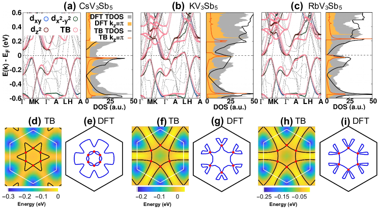
Our TB model can generically reproduce the DFT bands for various CDW stacking configurations. A specific set of TB parameters accurately replicates the DFT bands for the , , and orbitals (in global coordinates) near the Fermi level for both the -shifted and non--shifted stacking configurations of ISD or SD structures. Figures 2(a-c) depict the electronic band structures and the density of states obtained using both DFT and TB for the non--shifted ISD structure for all three alkali metals. Our TB bands (colored pink) closely match the DFT bands of vanadium , , and orbitals (colored blue, brown, and green, respectively) for all three alkali metals. The employed sets of TB parameters for V3Sb5 ( = K, Rb, and Cs) are presented in Table 1. The out-of-plane hopping parameters in our minimal vanadium TB models show substantial magnitudes, which effectively capture the three-dimensional nature of these systems. Notably, the nearest-neighbor (NN) hopping parameter along the out-of-plane direction, , is larger than the in-plane next-nearest-neighbor (NNN) hopping parameter, , for all three systems. Additionally, the NNNN out-of-plane hopping parameter is larger than the NNN out-of-plane hopping parameter , which we attribute to the weak overlap between the NNN sites.
| non--shift | non--shift | -shift | |
|---|---|---|---|
| ISD+ISD | SD+ISD | ISD+ISD | |
| CsV3Sb5 | 0.0 | 15.4 | -10.6 |
Our comprehensive DFT and TB calculations reveal a sharp peak in the DOS just below the Fermi level for the non--shifted ISD structure in all three compounds, mainly attributed to the VHS at . The constant energy contours in the plane, obtained by both DFT [Figs. 2(e,g,i)] and TB [Figs. 2(d,f,h)] calculations, show six symmetry-related van Hove saddle points, with one located along the direction and the other five along other symmetry-related high symmetry lines. The VHSs are identified by the crossing points (colored red) in the constant energy contour, which satisfy two conditions: (i) zero gradient of energy dispersion and (ii) a negative value of the Hessian determinant . These VHSs at the plane primarily contribute to the large DOS below the Fermi level, as consistently confirmed by both DFT and TB calculations [Figs. 2(a-c)], indicating that the , , and orbitals of vanadium atoms (in global coordinates) are responsible for electronic instabilities near the Fermi level in the non--shifted CDW order.
We conduct further analysis on the VHSs in the non--shifted ISD structure. The VHSs are classified as type-II, as they reside off time-reversal invariant momenta [31, 93, 94]. The explicitly calculated Hessian determinant values using TB models for these type-II VHSs are -0.327 eVÅ2, -1.716 eVÅ2, and -1.408 eVÅ2 for CsV3Sb5, KV3Sb5, and RbV3Sb5, respectively. The value is quite close to zero in the case of Cs, in line with the flat-like dispersion along the direction [Fig. 2(a)] and quasi-flat energy band landscape across broader regions near the A point [Fig. 2(d)], a distinct feature from the other two systems. Consequently, the VHSs in the ISD CDW phase in the CsV3Sb5 system are further characterized as higher-order-like VHSs, where a higher-order VHS is defined by a zero value of the Hessian determinant [94], serving as sources of diverse intriguing many-body phenomena [94, 95]. We note that both the type-II and higher-order like VHSs found in our study are different from those studied in the pristine phase at the plane in the monolayer limit [31] and in the bulk CsV3Sb5 system [29], respectively. This suggests that the VHSs still play an important role in stacking-dependent 3D CDW phases.
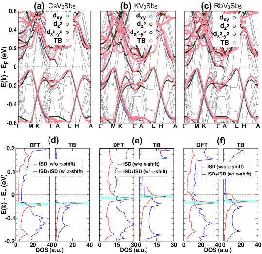
We examine the -phase shift stacking effect on the electronic structures of V3Sb5. We consider the -shifted ISD+ISD structure where alternating ISD layers along the -direction are relatively shifted by a -phase from each other [Fig. 1(g)]. The band dispersion and DOS for the -shifted ISD+ISD structure for all three alkali metals are shown in Fig. 3. The same TB parameters used for the non--shifted ISD structure yield TB bands in good agreement with the DFT bands of vanadium , , and orbitals [Figs. 3(a-c)]. To track the changes in energy bands under the -phase shift, we compare the energy bands at for the structure with those at both the and planes for the structure. This comparison is necessary because, when a -phase shift occurs, the energy bands at the plane in the CDW fold into the plane in the CDW, resulting in a doubling of the number of energy bands. The overall band dispersions at the plane of the ISD+ISD structure [Fig. 3(a-c)] are similar to those of the ISD structure at both the and planes [Figs. 2(a-c)]. However, a significant difference occurs in the flat-like dispersions along the line in the structure. In the structure, these flat-like dispersions become more dispersive under the -phase shift, as seen along the line. Consequently, the DOS in the -shifted ISD+ISD structure exhibits a depletion near the Fermi level compared to the non--shifted ISD structure, indicating the lifting of the VHSs due to the -phase shift [Figs. 3(d-f)]. This leads to electrons occupying lower energy levels, thereby stabilizing the -shifted structure. The in-plane , , and orbitals capture essential changes in the DOS under the out-of-plane -phase shift, highlighting their crucial roles in stabilizing the ground state 3D CDW order.
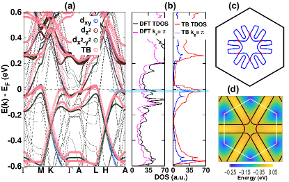
We finalize our discussion by speculating on the significance of our findings in alternating SD and ISD distorted layers, which are observed as part of the CDW structure in CsV3Sb5 [52, 67, 96]. The existence of the CDW structure in CsV3Sb5 was controversial, and was later found to be sensitive to growth conditions such as chemical disorder and thermal annealing [68, 69, 70]. For the structural model, initial experiment suggested alternating ISD layers followed by three SD distorted layers along the -direction without any -phase shift between adjacent kagomé layers [67]. However, subsequent studies [69, 70, 96] propose various stacking configurations, including complex stacking arrangements of ISD layers without alternating SD layers in the CDW structure. Our total energy calculations show that the -shift stacking remains favorable over the SD+ISD stacking (Table 3), consistent with previous DFT calculations [60, 69]. Our calculations of the band structure, DOS, and constant energy contour for CsV3Sb5 with alternating SD and ISD layers (Fig. 4), reveal a sharp DOS peak just below the Fermi level originating from the plane, attributed to the VHSs. This observation potentially supports the structural model with an ISD+ISD -shift structure, as the electronic instability is indicated in the alternating SD+ISD structure and the additional periodicity doubling along the -axis may relieve this diverging DOS at the Fermi level as in the case of the to transition.
4 Conclusion
Our comprehensive investigation, employing DFT and tight-binding calculations, delves into the stacking-dependent electronic structures of 3D CDW structures in V3Sb5. Our findings unveil the electronic origin of out-of-plane CDW ordering, highlighting the critical role of interlayer coupling in electronic instabilities near the Fermi level. A crucial aspect of our findings centers around the instability inherent in the ISD structure, attributed to the intense density of states originating from the plane at or near the Fermi level. This enhanced density of states is associated with the presence of type-II van Hove singularities. However, upon the 3D stacking of ISD layers along the -direction with a -phase shift, we observe a substantial renormalization of the density of states at the Fermi level, leading to the disappearance of the van Hove singularities and thus stabilizing the 3D -shifted ISD+ISD CDW ground state. Furthermore, our analysis highlights that the alternative stacking of ISD+SD layers in CsV3Sb5 also presents electronic instabilities near the Fermi level, making it energetically less favorable than the ISD+ISD -shifted configuration.
Additionally, we have formulated an effective 3D tight-binding model that captures the essential physics of V3Sb5 kagomé systems. This model serves as a valuable platform for further investigation of 3D interlayer coupling effects on novel phenomena observed in V3Sb5 kagomé metals. We anticipate that this approach will uncover new exotic physics beyond the current studies limited to 2D kagomé models, such as three-dimensional chiral flux order and three-dimensional electronic nematicity.
We conclude by comparing our study to a previous one [89, 97] that introduces a comprehensive tight-binding model for the four orbitals of V and the orbital of Sb, which is essential for describing the energies of four VHSs near the Fermi level in the plane under various strains and might be useful for describing all VHSs throughout the BZ. While this model is comprehensive, our simple model focuses on the orbitals and effectively describes the VHS that governs the low-energy electronic structure in the plane without 3D CDW. We believe our simplified TB theory offers a practical approach for future research on interacting Hamiltonians and complex systems, such as twisted bilayer V3Sb5 systems.
Data availability statement
All data are included within the article and its supplementary materials.
Declaration of competing interest
The authors declare that there are no competing financial interests or personal relationships that could have influenced the work reported in this paper.
Acknowledgments
Y.K. acknowledges the support from the National Research Foundation (NRF) of Korea under grant number NRF-2021R1A2C1013871. The Korea Institute of Science and Technology Information (KISTI) (KSC-2021-CRE-0116) provided the computational resource.
Appendix A. Supplementary data
Supplementary data to this article can be found online at
References
-
[1]
J.-W. Rhim, K. Kim, B.-J. Yang,
Quantum distance and
anomalous landau levels of flat bands, Nature 584 (7819) (2020) 59–63.
http://dx.doi.org/10.1038/s41586-020-2540-1 -
[2]
M. Li, D. Zhirihin, M. Gorlach, X. Ni, D. Filonov, A. Slobozhanyuk, A. Alù,
A. B. Khanikaev,
Higher-order topological
states in photonic kagome crystals with long-range interactions, Nat.
Photonics 14 (2) (2020) 89–94.
http://dx.doi.org/10.1038/s41566-019-0561-9 -
[3]
M. Kang, S. Fang, L. Ye, H. C. Po, J. Denlinger, C. Jozwiak, A. Bostwick,
E. Rotenberg, E. Kaxiras, J. G. Checkelsky, R. Comin,
Topological flat bands in
frustrated kagome lattice cosn, Nat. Commun. 11 (1) (2020) 4004.
http://dx.doi.org/10.1038/s41467-020-17465-1 -
[4]
W.-H. Ko, P. A. Lee, X.-G. Wen,
Doped kagome
system as exotic superconductor, Phys. Rev. B 79 (2009) 214502.
https://link.aps.org/doi/10.1103/PhysRevB.79.214502 -
[5]
S.-L. Yu, J.-X. Li,
Chiral
superconducting phase and chiral spin-density-wave phase in a hubbard model
on the kagome lattice, Phys. Rev. B 85 (2012) 144402.
https://link.aps.org/doi/10.1103/PhysRevB.85.144402 -
[6]
M. L. Kiesel, C. Platt, R. Thomale,
Unconventional
fermi surface instabilities in the kagome hubbard model, Phys. Rev. Lett.
110 (2013) 126405.
https://link.aps.org/doi/10.1103/PhysRevLett.110.126405 -
[7]
W.-S. Wang, Z.-Z. Li, Y.-Y. Xiang, Q.-H. Wang,
Competing
electronic orders on kagome lattices at van hove filling, Phys. Rev. B 87
(2013) 115135.
https://link.aps.org/doi/10.1103/PhysRevB.87.115135 -
[8]
S. Yan, D. A. Huse, S. R. White,
Spin-liquid ground state of
the kagome Heisenberg antiferromagnet, Science 332 (6034) (2011)
1173–1176.
http://dx.doi.org/10.1126/science.1201080 -
[9]
T.-H. Han, J. S. Helton, S. Chu, D. G. Nocera, J. A. Rodriguez-Rivera,
C. Broholm, Y. S. Lee,
Fractionalized excitations in
the spin-liquid state of a kagome-lattice antiferromagnet, Nature 492 (7429)
(2012) 406–410.
http://dx.doi.org/10.1038/nature11659 -
[10]
J.-X. Yin, B. Lian, M. Z. Hasan,
Topological kagome magnets
and superconductors, Nature 612 (7941) (2022) 647–657.
https://doi.org/10.1038/s41586-022-05516-0 -
[11]
M. Fu, T. Imai, T.-H. Han, Y. S. Lee,
Evidence for a
gapped spin-liquid ground state in a kagome Heisenberg antiferromagnet,
Science 350 (6261) (2015) 655–658.
https://www.science.org/doi/abs/10.1126/science.aab2120 -
[12]
Y. Zhou, K. Kanoda, T.-K. Ng,
Quantum spin
liquid states, Rev. Mod. Phys. 89 (2) (2017) 025003.
https://link.aps.org/doi/10.1103/RevModPhys.89.025003 -
[13]
M. Kang, L. Ye, S. Fang, J.-S. You, A. Levitan, M. Han, J. I. Facio,
C. Jozwiak, A. Bostwick, E. Rotenberg, et al.,
Dirac fermions and flat
bands in the ideal kagome metal FeSn, Nat. Mater. 19 (2) (2020) 163–169.
https://doi.org/10.1038/s41563-019-0531-0 -
[14]
Z. Lin, J.-H. Choi, Q. Zhang, W. Qin, S. Yi, P. Wang, L. Li, Y. Wang, H. Zhang,
Z. Sun, et al.,
Flatbands and
emergent ferromagnetic ordering in Fe3Sn2 kagome lattices, Phys.
Rev. Lett. 121 (9) (2018) 096401.
https://link.aps.org/doi/10.1103/PhysRevLett.121.096401 -
[15]
H. Huang, L. Zheng, Z. Lin, X. Guo, S. Wang, S. Zhang, C. Zhang, Z. Sun,
Z. Wang, H. Weng, et al.,
Flat-band-induced
anomalous anisotropic charge transport and orbital magnetism in kagome metal
CoSn, Phys. Rev. Lett. 128 (9) (2022) 096601.
https://link.aps.org/doi/10.1103/PhysRevLett.128.096601 -
[16]
B. R. Ortiz, L. C. Gomes, J. R. Morey, M. Winiarski, M. Bordelon, J. S. Mangum,
I. W. H. Oswald, J. A. Rodriguez-Rivera, J. R. Neilson, S. D. Wilson,
E. Ertekin, T. M. McQueen, E. S. Toberer,
New kagome
prototype materials: discovery of KV3Sb5, RbV3Sb5, and
CsV3Sb5, Phys. Rev. Mater. 3 (2019) 094407.
https://link.aps.org/doi/10.1103/PhysRevMaterials.3.094407 -
[17]
B. R. Ortiz, S. M. L. Teicher, Y. Hu, J. L. Zuo, P. M. Sarte, E. C. Schueller,
A. M. M. Abeykoon, M. J. Krogstad, S. Rosenkranz, R. Osborn, R. Seshadri,
L. Balents, J. He, S. D. Wilson,
CsV3Sb5:
A topological kagome metal with a superconducting ground
state, Phys. Rev. Lett. 125 (2020) 247002.
https://link.aps.org/doi/10.1103/PhysRevLett.125.247002 -
[18]
S. D. Wilson, B. R. Ortiz,
V3Sb5 kagome
superconductors, Nat. Rev. Mater. (2024).
https://doi.org/10.1038/s41578-024-00677-y -
[19]
H. Yang, Z. Zhao, X.-W. Yi, J. Liu, J.-Y. You, Y. Zhang, H. Guo, X. Lin,
C. Shen, H. Chen, et al.,
Titanium-based kagome superconductor
CsTi3Bi5 and topological states, arXiv preprint arXiv:2209.03840
(2022).
https://arxiv.org/abs/2209.03840 -
[20]
D. Werhahn, B. R. Ortiz, A. K. Hay, S. D. Wilson, R. Seshadri, D. Johrendt,
The kagomé metals
RbTi3Bi5 and CsTi3Bi5, Z. Naturforsch. B 77 (11-12) (2022)
757–764.
https://doi.org/10.1515/znb-2022-0125 -
[21]
B. Liu, M.-Q. Kuang, Y. Luo, Y. Li, C. Hu, J. Liu, Q. Xiao, X. Zheng, L. Huai,
S. Peng, et al.,
Tunable van
hove singularity without structural instability in kagome metal
CsTi3Bi5, Phys. Rev. Lett. 131 (2) (2023) 026701.
https://link.aps.org/doi/10.1103/PhysRevLett.131.026701 -
[22]
G. Pokharel, S. M. L. Teicher, B. R. Ortiz, P. M. Sarte, G. Wu, S. Peng, J. He,
R. Seshadri, S. D. Wilson,
Electronic
properties of the topological kagome metals YV6Sn6 and
GdV6Sn6, Phys. Rev. B 104 (2021) 235139.
https://link.aps.org/doi/10.1103/PhysRevB.104.235139 -
[23]
H. W. S. Arachchige, W. R. Meier, M. Marshall, T. Matsuoka, R. Xue, M. A.
McGuire, R. P. Hermann, H. Cao, D. Mandrus,
Charge density
wave in kagome lattice intermetallic ScV6Sn6, Phys. Rev. Lett.
129 (2022) 216402.
https://link.aps.org/doi/10.1103/PhysRevLett.129.216402 -
[24]
K. Wang, S. Chen, S.-W. Kim, B. Monserrat,
Origin of competing charge density
waves in kagome metal ScV6Sn6, arXiv preprint arXiv:2403.17058
(2024).
https://arxiv.org/abs/2403.17058 -
[25]
X. Teng, L. Chen, F. Ye, E. Rosenberg, Z. Liu, J.-X. Yin, Y.-X. Jiang, J. S.
Oh, M. Z. Hasan, K. J. Neubauer, B. Gao, Y. Xie, M. Hashimoto, D. Lu,
C. Jozwiak, A. Bostwick, E. Rotenberg, R. J. Birgeneau, J.-H. Chu, M. Yi,
P. Dai, Discovery of charge
density wave in a kagome lattice antiferromagnet, Nature 609 (7927) (2022)
490–495.
https://doi.org/10.1038/s41586-022-05034-z -
[26]
X. Teng, J. S. Oh, H. Tan, L. Chen, J. Huang, B. Gao, J.-X. Yin, J.-H. Chu,
M. Hashimoto, D. Lu, C. Jozwiak, A. Bostwick, E. Rotenberg, G. E. Granroth,
B. Yan, R. J. Birgeneau, P. Dai, M. Yi,
Magnetism and charge
density wave order in kagome fege, Nature Physics 19 (6) (2023) 814–822.
https://doi.org/10.1038/s41567-023-01985-w -
[27]
J.-X. Yin, Y.-X. Jiang, X. Teng, M. S. Hossain, S. Mardanya, T.-R. Chang,
Z. Ye, G. Xu, M. M. Denner, T. Neupert, B. Lienhard, H.-B. Deng, C. Setty,
Q. Si, G. Chang, Z. Guguchia, B. Gao, N. Shumiya, Q. Zhang, T. A. Cochran,
D. Multer, M. Yi, P. Dai, M. Z. Hasan,
Discovery of
charge order and corresponding edge state in kagome magnet FeGe, Phys.
Rev. Lett. 129 (2022) 166401.
https://link.aps.org/doi/10.1103/PhysRevLett.129.166401 -
[28]
X. Wu, T. Schwemmer, T. Müller, A. Consiglio, G. Sangiovanni, D. Di Sante,
Y. Iqbal, W. Hanke, A. P. Schnyder, M. M. Denner, M. H. Fischer, T. Neupert,
R. Thomale,
Nature of
unconventional pairing in the kagome superconductors V3Sb5
(), Phys. Rev. Lett. 127 (2021)
177001.
https://link.aps.org/doi/10.1103/PhysRevLett.127.177001 -
[29]
M. Kang, S. Fang, J.-K. Kim, B. R. Ortiz, S. H. Ryu, J. Kim, J. Yoo,
G. Sangiovanni, D. Di Sante, B.-G. Park, et al.,
Twofold van hove
singularity and origin of charge order in topological kagome superconductor
CsV3Sb5, Nat. Phys. 18 (3) (2022) 301–308.
https://doi.org/10.1038/s41567-021-01451-5 -
[30]
Y. Hu, X. Wu, B. R. Ortiz, S. Ju, X. Han, J. Ma, N. C. Plumb, M. Radovic,
R. Thomale, S. D. Wilson, A. P. Schnyder, M. Shi,
Rich nature of van hove
singularities in kagome superconductor CsV3Sb5, Nat. Commun.
13 (1) (2022) 2220.
https://doi.org/10.1038/s41467-022-29828-x -
[31]
S.-W. Kim, H. Oh, E.-G. Moon, Y. Kim,
Monolayer kagome metals
V3Sb5, Nat. Commun. 14 (1) (2023) 591.
https://doi.org/10.1038/s41467-023-36341-2 -
[32]
T. Neupert, M. M. Denner, J.-X. Yin, R. Thomale, M. Z. Hasan,
Charge order and
superconductivity in kagome materials, Nat. Phys. 18 (2) (2022) 137–143.
https://doi.org/10.1038/s41567-021-01404-y -
[33]
K. Jiang, T. Wu, J.-X. Yin, Z. Wang, M. Z. Hasan, S. D. Wilson, X. Chen, J. Hu,
Kagome superconductors
V3Sb5 ( K, Rb, Cs), Natl. Sci. Rev. 10 (2) (2022)
nwac199.
https://doi.org/10.1093/nsr/nwac199 -
[34]
S.-Y. Yang, Y. Wang, B. R. Ortiz, D. Liu, J. Gayles, E. Derunova,
R. Gonzalez-Hernandez, L. Šmejkal, Y. Chen, S. S. P. Parkin, S. D. Wilson,
E. S. Toberer, T. McQueen, M. N. Ali,
Giant,
unconventional anomalous hall effect in the metallic frustrated magnet
candidate, KV3Sb5, Sci. Adv. 6 (31) (2020) eabb6003.
https://www.science.org/doi/abs/10.1126/sciadv.abb6003 -
[35]
F. H. Yu, T. Wu, Z. Y. Wang, B. Lei, W. Z. Zhuo, J. J. Ying, X. H. Chen,
Concurrence of
anomalous hall effect and charge density wave in a superconducting
topological kagome metal, Phys. Rev. B 104 (2021) L041103.
https://link.aps.org/doi/10.1103/PhysRevB.104.L041103 -
[36]
B. R. Ortiz, P. M. Sarte, E. M. Kenney, M. J. Graf, S. M. L. Teicher,
R. Seshadri, S. D. Wilson,
Superconductivity
in the kagome metal KV3Sb5, Phys. Rev. Mater. 5
(2021) 034801.
https://link.aps.org/doi/10.1103/PhysRevMaterials.5.034801 -
[37]
Q. Yin, Z. Tu, C. Gong, Y. Fu, S. Yan, H. Lei,
Superconductivity and
normal-state properties of kagome metal RbV3Sb5 single crystals,
Chin. Phys. Lett. 38 (3) (2021) 037403.
https://dx.doi.org/10.1088/0256-307X/38/3/037403 -
[38]
Y.-X. Jiang, J.-X. Yin, M. M. Denner, N. Shumiya, B. R. Ortiz, G. Xu,
Z. Guguchia, J. He, M. S. Hossain, X. Liu, J. Ruff, L. Kautzsch, S. S. Zhang,
G. Chang, I. Belopolski, Q. Zhang, T. A. Cochran, D. Multer, M. Litskevich,
Z.-J. Cheng, X. P. Yang, Z. Wang, R. Thomale, T. Neupert, S. D. Wilson, M. Z.
Hasan, Unconventional
chiral charge order in kagome superconductor KV3Sb5, Nat. Mater.
20 (10) (2021) 1353–1357.
https://doi.org/10.1038/s41563-021-01034-y -
[39]
Y.-P. Lin, R. M. Nandkishore,
Complex charge
density waves at van hove singularity on hexagonal lattices: Haldane-model
phase diagram and potential realization in the kagome metals
V3Sb5 (K, Rb, Cs), Phys. Rev. B 104 (2021) 045122.
https://link.aps.org/doi/10.1103/PhysRevB.104.045122 -
[40]
T. Park, M. Ye, L. Balents,
Electronic
instabilities of kagome metals: Saddle points and Landau theory, Phys.
Rev. B 104 (2021) 035142.
https://link.aps.org/doi/10.1103/PhysRevB.104.035142 -
[41]
X. Feng, K. Jiang, Z. Wang, J. Hu,
Chiral
flux phase in the kagome superconductor V3Sb5, Sci. Bull.
66 (14) (2021) 1384–1388.
https://www.sciencedirect.com/science/article/pii/S2095927321003224 -
[42]
M. M. Denner, R. Thomale, T. Neupert,
Analysis of
charge order in the kagome metal V3Sb5, Phys. Rev. Lett. 127
(2021) 217601.
https://link.aps.org/doi/10.1103/PhysRevLett.127.217601 -
[43]
C. Mielke, D. Das, J.-X. Yin, H. Liu, R. Gupta, Y.-X. Jiang, M. Medarde, X. Wu,
H. C. Lei, J. Chang, P. Dai, Q. Si, H. Miao, R. Thomale, T. Neupert, Y. Shi,
R. Khasanov, M. Z. Hasan, H. Luetkens, Z. Guguchia,
Time-reversal
symmetry-breaking charge order in a kagome superconductor, Nature 602 (7896)
(2022) 245–250.
https://doi.org/10.1038/s41586-021-04327-z -
[44]
C. Guo, C. Putzke, S. Konyzheva, X. Huang, M. Gutierrez-Amigo, I. Errea,
D. Chen, M. G. Vergniory, C. Felser, M. H. Fischer, T. Neupert, P. J. W.
Moll, Switchable chiral
transport in charge-ordered kagome metal CsV3Sb5, Nature
611 (7936) (2022) 461–466.
https://doi.org/10.1038/s41586-022-05127-9 -
[45]
Y. Xu, Z. Ni, Y. Liu, B. R. Ortiz, Q. Deng, S. D. Wilson, B. Yan, L. Balents,
L. Wu, Three-state
nematicity and magneto-optical kerr effect in the charge density waves in
kagome superconductors, Nat. Phys. 18 (12) (2022) 1470–1475.
https://doi.org/10.1038/s41567-022-01805-7 -
[46]
Y. Xiang, Q. Li, Y. Li, W. Xie, H. Yang, Z. Wang, Y. Yao, H.-H. Wen,
Twofold symmetry of c-axis
resistivity in topological kagome superconductor CsV3Sb5 with
in-plane rotating magnetic field, Nat. Commun. 12 (1) (2021) 6727.
https://doi.org/10.1038/s41467-021-27084-z -
[47]
H. Li, H. Zhao, B. R. Ortiz, T. Park, M. Ye, L. Balents, Z. Wang, S. D. Wilson,
I. Zeljkovic, Rotation
symmetry breaking in the normal state of a kagome superconductor
KV3Sb5, Nat. Phys. 18 (3) (2022) 265–270.
https://doi.org/10.1038/s41567-021-01479-7 -
[48]
H. Luo, Q. Gao, H. Liu, Y. Gu, D. Wu, C. Yi, J. Jia, S. Wu, X. Luo, Y. Xu,
L. Zhao, Q. Wang, H. Mao, G. Liu, Z. Zhu, Y. Shi, K. Jiang, J. Hu, Z. Xu,
X. J. Zhou, Electronic
nature of charge density wave and electron-phonon coupling in kagome
superconductor KV3Sb5, Nat. Commun. 13 (1) (2022) 273.
https://doi.org/10.1038/s41467-021-27946-6 -
[49]
H. Li, H. Zhao, B. R. Ortiz, Y. Oey, Z. Wang, S. D. Wilson, I. Zeljkovic,
Unidirectional coherent
quasiparticles in the high-temperature rotational symmetry broken phase of
V3Sb5 kagome superconductors, Nat. Phys. 19 (5) (2023)
637–643.
https://doi.org/10.1038/s41567-022-01932-1 -
[50]
S. Wu, B. R. Ortiz, H. Tan, S. D. Wilson, B. Yan, T. Birol, G. Blumberg,
Charge density
wave order in the kagome metal CsV3Sb5 (Cs, Rb, K), Phys.
Rev. B 105 (2022) 155106.
https://link.aps.org/doi/10.1103/PhysRevB.105.155106 -
[51]
D. Wulferding, S. Lee, Y. Choi, Q. Yin, Z. Tu, C. Gong, H. Lei, S. Yousuf,
J. Song, H. Lee, T. Park, K.-Y. Choi,
Emergent
nematicity and intrinsic versus extrinsic electronic scattering processes in
the kagome metal CsV3Sb5, Phys. Rev. Res. 4 (2022) 023215.
https://link.aps.org/doi/10.1103/PhysRevResearch.4.023215 -
[52]
M. Kang, S. Fang, J. Yoo, B. R. Ortiz, Y. M. Oey, J. Choi, S. H. Ryu, J. Kim,
C. Jozwiak, A. Bostwick, E. Rotenberg, E. Kaxiras, J. G. Checkelsky, S. D.
Wilson, J.-H. Park, R. Comin,
Charge order landscape and
competition with superconductivity in kagome metals, Nat. Mater. 22 (2)
(2023) 186–193.
https://doi.org/10.1038/s41563-022-01375-2 -
[53]
Q. Wu, Z. X. Wang, Q. M. Liu, R. S. Li, S. X. Xu, Q. W. Yin, C. S. Gong, Z. J.
Tu, H. C. Lei, T. Dong, N. L. Wang,
Simultaneous
formation of two-fold rotation symmetry with charge order in the kagome
superconductor CsV3Sb5 by optical polarization rotation
measurement, Phys. Rev. B 106 (2022) 205109.
https://link.aps.org/doi/10.1103/PhysRevB.106.205109 -
[54]
Z. Jiang, H. Ma, W. Xia, Z. Liu, Q. Xiao, Z. Liu, Y. Yang, J. Ding, Z. Huang,
J. Liu, Y. Qiao, J. Liu, Y. Peng, S. Cho, Y. Guo, J. Liu, D. Shen,
Observation of electronic
nematicity driven by the three-dimensional charge density wave in kagome
lattice KV3Sb5, Nano Lett. 23 (12) (2023) 5625–5633.
https://doi.org/10.1021/acs.nanolett.3c01151 -
[55]
L. Nie, K. Sun, W. Ma, D. Song, L. Zheng, Z. Liang, P. Wu, F. Yu, J. Li,
M. Shan, D. Zhao, S. Li, B. Kang, Z. Wu, Y. Zhou, K. Liu, Z. Xiang, J. Ying,
Z. Wang, T. Wu, X. Chen,
Charge-density-wave-driven
electronic nematicity in a kagome superconductor, Nature 604 (7904) (2022)
59–64.
https://doi.org/10.1038/s41586-022-04493-8 -
[56]
Y. Sur, K.-T. Kim, S. Kim, K. H. Kim,
Optimized superconductivity
in the vicinity of a nematic quantum critical point in the kagome
superconductor Cs(V1-xTix)3Sb5, Nat. Commun. 14 (1)
(2023) 3899.
https://doi.org/10.1038/s41467-023-39495-1 -
[57]
K. Chen, N. Wang, Q. Yin, Y. Gu, K. Jiang, Z. Tu, C. Gong, Y. Uwatoko, J. Sun,
H. Lei, et al.,
Double
superconducting dome and triple enhancement of Tc in the kagome
superconductor CsV3Sb5 under high pressure, Phys. Rev. Lett.
126 (24) (2021) 247001.
https://link.aps.org/doi/10.1103/PhysRevLett.126.247001 -
[58]
F. H. Yu, D. H. Ma, W. Z. Zhuo, S. Q. Liu, X. K. Wen, B. Lei, J. J. Ying, X. H.
Chen, Unusual competition
of superconductivity and charge-density-wave state in a compressed
topological kagome metal, Nature Communications 12 (1) (2021) 3645.
https://doi.org/10.1038/s41467-021-23928-w -
[59]
L. Zheng, Z. Wu, Y. Yang, L. Nie, M. Shan, K. Sun, D. Song, F. Yu, J. Li,
D. Zhao, S. Li, B. Kang, Y. Zhou, K. Liu, Z. Xiang, J. Ying, Z. Wang, T. Wu,
X. Chen, Emergent charge
order in pressurized kagome superconductor CsV3Sb5, Nature
611 (7937) (2022) 682–687.
https://doi.org/10.1038/s41586-022-05351-3 -
[60]
H. Tan, Y. Liu, Z. Wang, B. Yan,
Charge density
waves and electronic properties of superconducting kagome metals, Phys. Rev.
Lett. 127 (4) (2021) 046401.
https://link.aps.org/doi/10.1103/PhysRevLett.127.046401 -
[61]
H. Li, T. Zhang, T. Yilmaz, Y. Pai, C. Marvinney, A. Said, Q. Yin, C. Gong,
Z. Tu, E. Vescovo, et al.,
Observation of
unconventional charge density wave without acoustic phonon anomaly in kagome
superconductors V3Sb5 ( Rb, Cs), Phys. Rev. X 11 (3)
(2021) 031050.
https://link.aps.org/doi/10.1103/PhysRevX.11.031050 -
[62]
A. Ptok, A. Kobiałka, M. Sternik, J. Łażewski, P. T. Jochym, A. M. Oleś,
P. Piekarz,
Dynamical study
of the origin of the charge density wave in
(, Rb, Cs)
compounds, Phys. Rev. B 105 (2022) 235134.
https://link.aps.org/doi/10.1103/PhysRevB.105.235134 -
[63]
C. Wang, S. Liu, H. Jeon, J.-H. Cho,
Origin of charge
density wave in the layered kagome metal CsV3Sb5, Phys. Rev. B 105
(2022) 045135.
https://link.aps.org/doi/10.1103/PhysRevB.105.045135 -
[64]
G. Liu, X. Ma, K. He, Q. Li, H. Tan, Y. Liu, J. Xu, W. Tang, K. Watanabe,
T. Taniguchi, L. Gao, Y. Dai, H.-H. Wen, B. Yan, X. Xi,
Observation of
anomalous amplitude modes in the kagome metal CsV3Sb5, Nat Commun
13 (1) (2022) 3461.
https://www.nature.com/articles/s41467-022-31162-1 -
[65]
G. He, L. Peis, E. F. Cuddy, Z. Zhao, D. Li, Y. Zhang, R. Stumberger,
B. Moritz, H. Yang, H. Gao, T. P. Devereaux, R. Hackl,
Anharmonic
strong-coupling effects at the origin of the charge density wave in
CsV3Sb5, Nat Commun 15 (1) (2024) 1895.
https://www.nature.com/articles/s41467-024-45865-0 -
[66]
M. Gutierrez-Amigo, Ð. Dangić, C. Guo, C. Felser, P. J. Moll, M. G.
Vergniory, I. Errea, Phonon collapse
and anharmonic melting of the 3D charge-density wave in kagome metals,
arXiv preprint arXiv:2311.14112 (2023).
https://arxiv.org/abs/2311.14112 -
[67]
B. R. Ortiz, S. M. Teicher, L. Kautzsch, P. M. Sarte, N. Ratcliff, J. Harter,
J. P. Ruff, R. Seshadri, S. D. Wilson,
Fermi surface
mapping and the nature of charge-density-wave order in the kagome
superconductor CsV3Sb5, Phys. Rev. X 11 (4) (2021) 041030.
https://link.aps.org/doi/10.1103/PhysRevX.11.041030 -
[68]
Q. Stahl, D. Chen, T. Ritschel, C. Shekhar, E. Sadrollahi, M. Rahn, O. Ivashko,
M. v. Zimmermann, C. Felser, J. Geck,
Temperature-driven
reorganization of electronic order in CsV3Sb5, Phys. Rev. B
105 (19) (2022) 195136.
https://link.aps.org/doi/10.1103/PhysRevB.105.195136 -
[69]
Q. Xiao, Y. Lin, Q. Li, X. Zheng, S. Francoual, C. Plueckthun, W. Xia, Q. Qiu,
S. Zhang, Y. Guo, et al.,
Coexistence
of multiple stacking charge density waves in kagome superconductor
CsV3Sb5, Phys. Rev. Res. 5 (1) (2023) L012032.
https://link.aps.org/doi/10.1103/PhysRevResearch.5.L012032 -
[70]
L. Kautzsch, B. R. Ortiz, K. Mallayya, J. Plumb, G. Pokharel, J. P. Ruff,
Z. Islam, E.-A. Kim, R. Seshadri, S. D. Wilson,
Structural
evolution of the kagome superconductors V3Sb5 ( K, Rb,
and Cs) through charge density wave order, Phys. Rev. Mater. 7 (2) (2023)
024806.
https://link.aps.org/doi/10.1103/PhysRevMaterials.7.024806 - [71] R. Markiewicz, A survey of the van hove scenario for high-tc superconductivity with special emphasis on pseudogaps and striped phases, Journal of Physics and Chemistry of Solids 58 (8) (1997) 1179–1310.
-
[72]
K. Kim, S. Kim, J. S. Kim, H. Kim, J.-H. Park, B. I. Min,
Importance of the
van hove singularity in superconducting , Phys. Rev. B
97 (2018) 165102.
doi:10.1103/PhysRevB.97.165102.
https://link.aps.org/doi/10.1103/PhysRevB.97.165102 -
[73]
W. Wan, R. Harsh, P. Dreher, F. de Juan, M. M. Ugeda,
Superconducting dome by
tuning through a van hove singularity in a two-dimensional metal, npj 2D
Materials and Applications 7 (2023) 41.
doi:10.1038/s41699-023-00401-4.
http://dx.doi.org/10.1038/s41699-023-00401-4 -
[74]
V. Y. Irkhin, A. A. Katanin, M. I. Katsnelson,
Effects of van
hove singularities on magnetism and superconductivity in the
hubbard model: A parquet approach,
Phys. Rev. B 64 (2001) 165107.
doi:10.1103/PhysRevB.64.165107.
https://link.aps.org/doi/10.1103/PhysRevB.64.165107 -
[75]
I. I. Mazin, D. J. Singh,
Electronic structure
and magnetism in ru-based perovskites, Phys. Rev. B 56 (1997) 2556–2571.
doi:10.1103/PhysRevB.56.2556.
https://link.aps.org/doi/10.1103/PhysRevB.56.2556 -
[76]
H. Yamase, V. Oganesyan, W. Metzner,
Mean-field theory
for symmetry-breaking fermi surface deformations on a square lattice, Phys.
Rev. B 72 (2005) 035114.
doi:10.1103/PhysRevB.72.035114.
https://link.aps.org/doi/10.1103/PhysRevB.72.035114 -
[77]
G. Kresse, J. Hafner,
Ab initio molecular
dynamics for liquid metals, Phys. Rev. B 47 (1993) 558–561.
https://link.aps.org/doi/10.1103/PhysRevB.47.558 -
[78]
G. Kresse, J. Furthmüller,
Efficiency
of ab-initio total energy calculations for metals and semiconductors using a
plane-wave basis set, Computer. Mater. Sci. 6 (1) (1996) 15–50.
http://www.sciencedirect.com/science/article/pii/0927025696000080 -
[79]
G. Kresse, J. Furthmüller,
Efficient iterative
schemes for ab initio total-energy calculations using a plane-wave basis
set, Phys. Rev. B 54 (16) (1996) 11169.
https://link.aps.org/doi/10.1103/PhysRevB.54.11169 -
[80]
G. Kresse, D. Joubert,
From ultrasoft
pseudopotentials to the projector augmented-wave method, Phys. Rev. B 59
(1999) 1758–1775.
https://link.aps.org/doi/10.1103/PhysRevB.59.1758 -
[81]
J. P. Perdew, K. Burke, M. Ernzerhof,
Generalized
gradient approximation made simple, Phys. Rev. Lett. 77 (18) (1996) 3865.
https://link.aps.org/doi/10.1103/PhysRevLett.77.3865 -
[82]
P. E. Blöchl,
Projector
augmented-wave method, Phys. Rev. B 50 (24) (1994) 17953.
https://link.aps.org/doi/10.1103/PhysRevB.50.17953 -
[83]
S. Grimme, J. Antony, S. Ehrlich, H. Krieg,
A consistent and accurate ab initio
parametrization of density functional dispersion correction (DFT-D) for the
94 elements H-Pu, J. Chem. Phys. 132 (15) (2010) 154104.
https://doi.org/10.1063/1.3382344 -
[84]
G. Pizzi, V. Vitale, R. Arita, S. Blügel, F. Freimuth, G. Géranton,
M. Gibertini, D. Gresch, C. Johnson, T. Koretsune, J. Ibañez-Azpiroz,
H. Lee, J.-M. Lihm, D. Marchand, A. Marrazzo, Y. Mokrousov, J. I. Mustafa,
Y. Nohara, Y. Nomura, L. Paulatto, S. Poncé, T. Ponweiser, J. Qiao,
F. Thöle, S. S. Tsirkin, M. Wierzbowska, N. Marzari, D. Vanderbilt,
I. Souza, A. A. Mostofi, J. R. Yates,
Wannier90 as a community
code: new features and applications, J. Phys. Condens. Matter 32 (16) (2020)
165902.
https://dx.doi.org/10.1088/1361-648X/ab51ff -
[85]
N. Marzari, D. Vanderbilt,
Maximally localized
generalized wannier functions for composite energy bands, Phys. Rev. B 56
(1997) 12847–12865.
https://link.aps.org/doi/10.1103/PhysRevB.56.12847 -
[86]
I. Souza, N. Marzari, D. Vanderbilt,
Maximally
localized wannier functions for entangled energy bands, Phys. Rev. B 65
(2001) 035109.
https://link.aps.org/doi/10.1103/PhysRevB.65.035109 -
[87]
N. Marzari, A. A. Mostofi, J. R. Yates, I. Souza, D. Vanderbilt,
Maximally
localized wannier functions: Theory and applications, Rev. Mod. Phys. 84
(2012) 1419–1475.
https://link.aps.org/doi/10.1103/RevModPhys.84.1419 -
[88]
M. Kawamura,
Fermisurfer:
Fermi-surface viewer providing multiple representation schemes, Comput.
Phys. Commun. 239 (2019) 197–203.
https://www.sciencedirect.com/science/article/pii/S0010465519300347 -
[89]
M. Y. Jeong, H.-J. Yang, H. S. Kim, Y. B. Kim, S. Lee, M. J. Han,
Crucial role of
out-of-plane sb orbitals in van hove singularity formation and electronic
correlations in the superconducting kagome metal CsV3Sb5, Phys. Rev. B 105 (2022) 235145.
https://link.aps.org/doi/10.1103/PhysRevB.105.235145 -
[90]
H. Li, X. Liu, Y. B. Kim, H.-Y. Kee,
Origin of
-shifted three-dimensional charge density waves in kagome metal
AV3Sb5, Phys. Rev. B 108 (2023) 075102.
https://link.aps.org/doi/10.1103/PhysRevB.108.075102 -
[91]
J. Deng, R. Zhang, Y. Xie, X. Wu, Z. Wang,
Two elementary
band representation model, fermi surface nesting, and surface topological
superconductivity in AV3Sb5 ( K, Rb, Cs), Phys. Rev. B 108
(2023) 115123.
https://link.aps.org/doi/10.1103/PhysRevB.108.115123 -
[92]
A. Subedi,
Hexagonal-to-base-centered-orthorhombic
4Q charge density wave order in kagome metals KV3Sb5,
RbV3Sb5, CsV3Sb5, Phys. Rev. Materials 6 (1) (2022)
015001.
https://link.aps.org/doi/10.1103/PhysRevMaterials.6.015001 -
[93]
H. Yao, F. Yang,
Topological
odd-parity superconductivity at type-II two-dimensional van hove
singularities, Phys. Rev. B 92 (2015) 035132.
https://link.aps.org/doi/10.1103/PhysRevB.92.035132 -
[94]
N. F. Q. Yuan, H. Isobe, L. Fu,
Magic of high-order van
hove singularity, Nat. Commun. 10 (1) (Dec. 2019).
http://dx.doi.org/10.1038/s41467-019-13670-9 -
[95]
L. Classen, J. J. Betouras, High-order
Van Hove singularities and their connection to flat bands, arXiv preprint
arXiv:2405.20226 (2024).
https://arxiv.org/abs/2405.20226 -
[96]
Y. Hu, X. Wu, B. R. Ortiz, X. Han, N. C. Plumb, S. D. Wilson, A. P. Schnyder,
M. Shi, et al.,
Coexistence of
trihexagonal and star-of-david pattern in the charge density wave of the
kagome superconductor V3Sb5, Phys. Rev. B 106 (24) (2022)
L241106.
https://link.aps.org/doi/10.1103/PhysRevB.106.L241106 -
[97]
S. Sim, M. Y. Jeong, H. Lee, D. H. D. Lee, M. J. Han,
Chemical effect on the van hove
singularity in superconducting kagome metal AV3Sb5 ( K, Rb, and Cs),
Physical Chemistry Chemical Physics 26 (15) (2024) 11715–11721.
http://dx.doi.org/10.1039/D4CP00517A