Enhancement of Photoresponse for InGaAs Infrared Photodetectors Using Plasmonic WO3-x/CsyWO3-x Nanocrystals
Abstract
Fast and accurate detection of light in the near-infrared (NIR) spectral range plays a crucial role in modern society, from alleviating speed and capacity bottlenecks in optical communications to enhancing the control and safety of autonomous vehicles through NIR imaging systems. Several technological platforms are currently under investigation to improve NIR photodetection, aiming to surpass the performance of established III-V semiconductor p-i-n (PIN) junction technology. These platforms include in situ-grown inorganic nanocrystals and nanowire arrays, as well as hybrid organic-inorganic materials such as graphene-perovskite heterostructures. However, challenges remain in nanocrystal and nanowire growth, large-area fabrication of high-quality 2D materials, and the fabrication of devices for practical applications. Here, we explore the potential for tailored semiconductor nanocrystals to enhance the responsivity of planar metal-semiconductor-metal (MSM) photodetectors. MSM technology offers ease of fabrication and fast response times compared to PIN detectors. We observe enhancement of the optical-to-electric conversion efficiency by up to a factor of 2.5 through the application of plasmonically-active semiconductor nanorods and nanocrystals. We present a protocol for synthesizing and rapidly testing the performance of non-stoichiometric tungsten oxide (WO3-x) nanorods and cesium-doped tungsten oxide (CsyWO3-x) hexagonal nanoprisms prepared in colloidal suspensions and drop-cast onto photodetector surfaces. The results demonstrate the potential for a cost-effective and scalable method exploiting tailored nanocrystals to improve the performance of NIR optoelectronic devices.
Keywords: NIR photodetectors, NIR plasmonics, MSM photodetectors, Nanocrystals, Nanorods, WO3-x, CsyWO3-x, InGaAs, InAlAs
1 Introduction
Light detection in the near-infrared (NIR) and infrared (IR) wavelength ranges has numerous applications in fields such as biomedical imaging and sensing, thermal imaging, and telecommunications [1, 2, 3, 4, 5, 6]. Initially, mesoscopic-scale inorganic semiconducting materials were the primary candidates for developing faster, smaller, and more sensitive detectors. However, recent efforts have shifted towards engineering inorganic, organic, and hybrid inorganic/organic semiconducting nanostructures to significantly enhance performance, reduce device size, and create flexible form factor devices for industrial applications [7, 8, 5]. Promising approaches include designing III-V semiconductor nanowires, in situ-grown metal/semiconductor nanoparticles, and utilizing chemical vapor deposition or exfoliation techniques to produce 2D inorganic graphene/perovskite structures for optoelectronic devices [7, 9, 10].
During the past few decades, interest in the physics and applications of IR photodetectors with a tunable band gap for telecommunication wavelengths (m) has grown, especially those based on III-V semiconductors such as InGaAs [11, 12]. Several InGaAs photodetector designs are commonly studied, such as PN or PIN junctions, avalanche, and metal-semiconductor-metal (MSM) photodetectors [12]. MSM detectors are desirable for telecommunication applications due to their fast response times and ease of fabrication and integration with other electronics [13, 14, 15, 16, 17, 18].
A standard MSM photodetector consists of interdigitated metallic electrodes deposited on an active layer, such as InGaAs, forming two Schottky junctions in series. A finger electrode design is often chosen for simplicity of the device, both in terms of fabrication and characterization. MSM detectors can suffer from large dark currents due to relatively low Schottky barriers, however, this can be mitigated by introducing a lattice-matched InAlAs top layer to increase the barrier height. Performance improvements have been achieved through band gap tuning via InxGa1-xAs alloy concentration, Schottky barrier enhancement, and superlattice structures [19, 16, 12]. In this paper, we explore the use of plasmonic semiconductor nanocrystals to enhance the optical-to-electrical conversion efficiency of InGaAs MSM photodetectors, as measured by responsivity in the wavelength range of m.
Plasmonics primarily focuses on the generation, propagation, and detection of plasmonic waves, which are collective electronic excitations resulting from the interaction between an electromagnetic (EM) field and a metal/dielectric interface [20, 21, 22]. When EM waves interact with a metallic surface, a coherent charge density oscillation coupled to the EM field arises, known as a surface plasmon. Strong nanoscale confinement leads to localized surface plasmon resonances (LSPRs), characterized by discrete optical absorption bands and electric fields orders of magnitude larger than those associated with free space EM waves. Given their nanoscale dimensions, integration of plasmonic nanostructures with micro- and nanoelectronic devices is possible, and holds the potential to enhance device performance or realize novel functionalities.
Conductors with sub-wavelength dimensions support LSPRs, whose resonance frequencies depend on the geometry and free carrier density of the nanostructure, as well as its orientation with respect to the polarization of the EM field. Depending on the material, LSPRs can span from the ultraviolet (UV) to the far-infrared. Upon illumination, nanoscale regions of strong EM field enhancement, referred to as hot-spots, are generated at the surface of the structure. Plasmonics have been widely used to enhance the performance of photodetector and photovoltaic devices [23, 24, 25, 26, 27, 28, 29]. The enhanced EM field surrounding nanostructures can be harnessed in optoelectronic devices by generating LSPRs to improve responsivity across a broad range of frequencies. LSPR mechanisms that contribute to enhanced responsivity include: 1) increased concentration of the incident EM field and extended optical path length within the semiconductor, thereby enhancing photon absorption, and 2) plasmonic energy transfer from the nanostructure to the semiconductor through direct electron transfer [30]. Because of these broadband optical properties, plasmonic nanostructures have found use in a variety of applications including catalysis, medicine, surface chemistry, solar cells and sensing [20, 21, 22, 31, 32, 33, 34, 35, 36, 37].
Typically, Au and Ag nanoparticles (NPs) exhibit strong LSPRs and are used as plasmonic materials in the visible [38] or UV [39, 40, 41] spectral ranges. An emerging area of interest focuses on identifying high performance plasmonic materials compatible with other frequency ranges of interest, from NIR to terahertz [42, 43, 44, 45]. Fundamentally, the physics of LSPR does not change in the IR compared to the visible region, but the material requirements are dramatically different. The optical resonances in Au and Ag can be tuned to a degree by changing the size and shape of nanostructures, but the charge carrier densities (1022 cm-3) that primarily determine the the plasmonic frequency response are fixed. NIR applications require materials with lower carrier concentrations compared to metals, such as degenerately doped or non-stoichiometric semiconductors [46, 47, 48, 49]. There have been several reports on the use of materials such as transition metal oxides [50, 51], nitrides [52] and doped semiconductors [53] for IR plasmonic photodetectors.
Two candidate materials for IR plasmonics are WO3-x [44] and CsyWO3-x [45] nanocrystals (NCs). Compared to commonly used plasmonic Au/Ag nanostructures exhibiting LSPR in the UV-visible region, both WO3-x and CsyWO3-x possess visible-NIR LSPR due to their lower carrier densities, in the range of 1018-1022 cm-3. These materials are known to have optical absorption in the NIR, but their effectiveness as plasmonic materials for enhancement of responsivity in a photodetector has not yet been thoroughly investigated; only one recent study has investigated photodetector enhancement in the visible light range using WO3-x nanowire arrays [44]. The carrier densities of these materials can also be tuned via the chemical synthesis procedure (e.g., extrinsic doping). However, a potential challenge when using WO3-x and CsyWO3-x NCs, despite being environmentally benign, is their rate of oxidation in air. Oxidation degrades the carrier concentration over time or with exposure to higher temperatures, which may lead to changes in crystal structure by reducing the oxygen vacancy concentration, and thus the carrier density.
In this paper, we characterize the performance of InGaAs MSM photodetectors operating in the NIR modified by drop-cast WO3-x nanorods and CsyWO3-x hexagonal prisms. Clear enhancements of responsivity by up to a factor 2.5, broadly consistent with the plasmonic absorption spectra of the NCs, are observed. These results indicate that suitably prepared conductive metal oxide NCs are a promising family of materials for IR plasmonic applications.
2 Materials and Methods
2.1 Molecular Beam Epitaxy of InGaAs Heterostructures
The InGaAs heterostructure shown in figure 1(a) was grown by molecular beam epitaxy (MBE). Prior to growth, a 2”, semi-insulating (Fe-doped), double-side polished InP(001) substrate was heated to 520C for approximately 10 minutes to desorb surface oxides. Epitaxy of the InAlAs/InGaAs/InAlAs layers was carried out at a substrate temperature of 470C. Both the In0.53Ga0.47As and In0.52Al0.48As layers were grown at a rate of 2.5 Å/s.
2.2 Nanocrystal Synthesis
2.2.1 Materials
All chemicals were used as received, with no further purification. W(CO)6 (97 %) and HPLC-grade tetrachloroethylene (TCE) ( 99.5 %) were purchased from Thermo Scientific, WCl4 (95 %), CsCl (95 %) from Kodak, technical-grade oleic acid (OlAc, 90 %) and oleylamine (OlAm, 70 %), HPLC-grade acetone ( 99.9 %), toluene ( 99.9 %), and hexane ( 98.5 %) were all purchased from Sigma Aldrich.
2.2.2 Synthesis of WO3-x
Substoichiometric tungsten oxide (WO3-x) NCs were synthesized following the thermal decomposition synthesis procedure for tungsten NPs reported by Sahoo et al. [54], with minor modifications as previously reported [55]. Briefly, 7.626 g of OlAc, 2.415 g of OlAm, and 1.057 g of W(CO)6 precursor were mixed inside a reaction vessel and degassed for 30 minutes. Using a standard Schlenk line technique, the vessel was purged with nitrogen gas, then the reaction mixture was heated to 300 ∘C at a rate of 0.5 ∘C/s. After 2 hours at 300 ∘C, the vessel was removed from the heating mantle and naturally cooled to room temperature. The blue-color reaction mixture, indicating the presence of WO3-x NCs, was purified three times using toluene and ethanol in 1:1 volumetric ratio. After each washing cycle, the samples were centrifuged at 3000 RPM for 5 min at room temperature. After final purification, the WO3-x NCs were dispersed in 5 mL of toluene. For the optical extinction measurements, 1 mL of the toluene dispersion was precipitated once again using the above method and redispersed in 1 mL of TCE. All the colloidal dispersions were stored under N2 atmosphere until further use.
2.2.3 Synthesis of CsyWO3-x
Hexagonal CsyWO3-x NCs were synthesized using the synthesis method reported by Mattox et al. [56] with minor modifications. The solid precursors (0.20 mmol of WCl4 and 0.12 mmol of CsCl) were added into a mixture of OlAc (8.95 g) and OlAm (0.267 g), which was then degassed for approximately 20 min at 120 ∘C. The reaction mixture was then heated to 300 ∘C and kept at that temperature. After 2 hours, the reaction mixture was cooled down to room temperature, and the dark blue product obtained was pipetted into centrifuge tubes. NCs were washed with toluene and acetone in approximately 1:1 volumetric ratio applying vortex mixing for 5 minutes, then the sample was centrifuged at 7830 RPM for 5 min to separate the NCs from the supernatant. Similar to the WO3-x NCs, the as-prepared CsyWO3-x NCs were suspended in toluene or TCE for optical measurements and stored under N2 atmosphere until further use.
2.3 Photodetector Fabrication
A 2 cm 2 cm die from the as-grown InGaAs heterostructure wafer was cleaned by sonication in acetone and isopropyl alcohol (IPA) for 2 minutes each. Polydimethylglutarimide polymer (PMGI) and Shipley 1813 positive photoresists were deposited by spin coating at 5000 RPM for 60 seconds to create a homogeneous bilayer approximately 1.3 m thick. The resist is baked at 120∘C for 90 seconds, followed by optical lithography performed using a Heidelberg instruments MLA150 maskless aligner to pattern the interdigitated electrodes and bond pads. The patterned resist was developed in a metal free optical developer (MF-319) for 100 seconds followed by a 20 second plasma ash to remove traces of resist residue from the exposed areas. A 1 minute HF etch was performed to remove surface oxides prior to deposition of 20/80nm of Ti/Au via electron beam evaporation. Metal liftoff was performed by leaving the sample overnight in Remover PG followed by rinsing in acetone and IPA. A schematic of the interdigitated electrode geometry is shown in figure 1(b).
2.4 Characterization of Nanocrystals
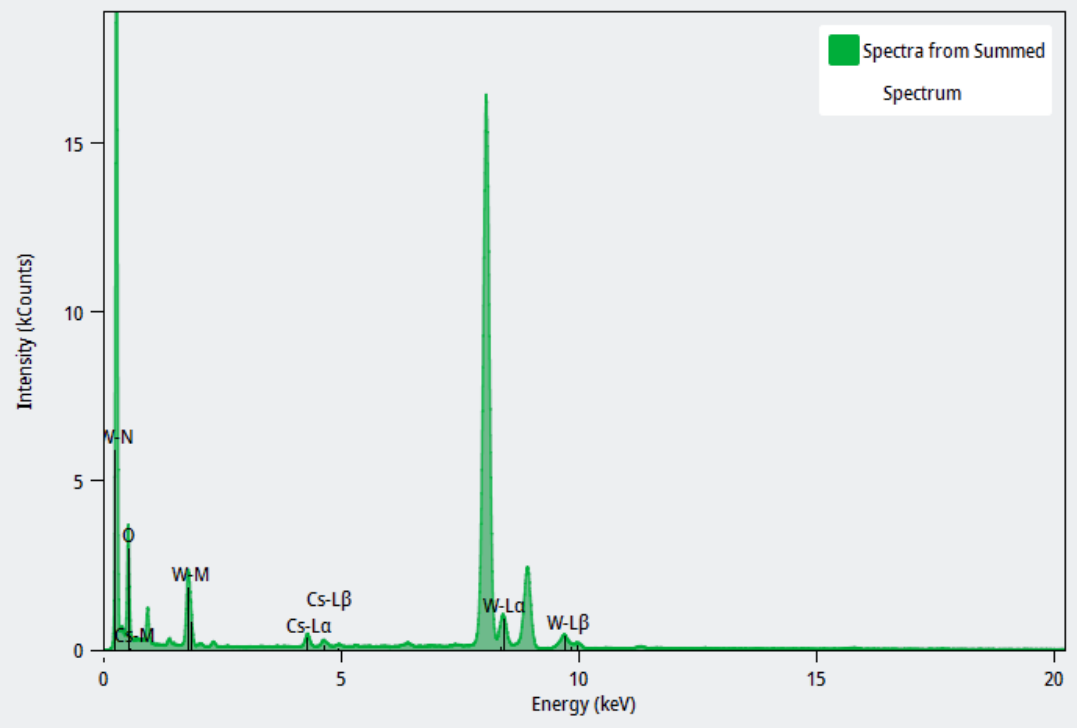
X-ray diffractometry (XRD) was performed to study the crystallinity and phase of the synthesized NCs using a Rigaku MiniFlex II Diffractometer equipped with a Cu K1 radiation source ( = 1.54056 Å). Transmission electron microscopy (TEM) measurements were performed to investigate the NC morphology using a JEOL-2010F instrument operating at 200 kV. The optical extinction spectra of the colloidal NC dispersions in TCE or NC thin films were performed to characterize the resonant wavelengths, absorption peak widths, and overall spectral shape using a Varian Cary 5000 UV-vis-NIR spectrophotometer. The synthesis and optical properties of the WO3-x and CsyWO3-x NCs in this work were found to be highly reproducible (see Figures S4-S5 in Supplementary Information).
2.5 Photocurrent Measurement Setup
Photodetectors are characterized using a custom setup that enables photocurrent measurements as a function of bias voltage and incident wavelength of light from the visible to the near-IR. The setup also enables characterization of the power spectrum of the light source, which is necessary for proper normalization of the measured photodetector responsivity. A schematic of the setup is shown in figure 2.
A Thorlabs SLS402 Mercury-Xenon short-arc light source generates a broadband spectrum ranging from 240 nm-2.4 m that is collimated and focused using a Thorlabs LA4464-f = 60.0 mm UV fused plano-convex uncoated lens into the 2 mm aperture entrance slit of a Sciencetech monochromator. A desired wavelength is selected by choosing one of the three Blaze gratings inside the monochromator and rotating the grating into to proper position with respect to the incident beam. The wavelength ranges for each of the three gratings are 100-700 nm, 700-1500 nm, and 1500-3500 nm. The diffracted beam for a selected wavelength then passes through a 2 mm aperture exit slit, FEL1400 or FEL0750 longpass filters to prevent higher-order diffracted wavelength modes, and is then focused using a Thorlabs LA5370-f = 40.0 nm CaF2 plano-convex uncoated lens through a post-mounted iris diaphragm onto the sample focal plane.
Photodetector devices are attached to a printed circuit board and wire bonded to Au plated pins that connect to an external circuit through a custom socket. The sample mount is fixed to a lateral (XY) translation stage assembled from Thorlabs single-axis PT1 and PT series components to facilitate alignment of a chosen detector with the beam. A Keithley 230 programmable voltage source supplies a bias voltage to the source/drain electrodes of a detector. Current is measured using a DL instruments 1212 current-voltage amplifier, with the output signal fed into an Agilent 34401A digital multimeter. The monochromator and the voltage source are computer-controlled using a custom written LabView program.
2.5.1 Responsivity Measurement Protocol
The broadband light source is switched on for 1 hour to reach a stable operating temperature and ensure stability of the output spectrum. Prior to measuring the photodetector spectral responsivity, a Thorlabs 700-1800 nm, 50 nW-40 mW Ge photodiode power sensor is used to obtain the power spectrum of the light source. The power sensor is placed in the focal plane behind the post-mounted iris diaphragm and the FEL0750 filter is placed in between the monochromator and LA5370 focusing lens. The power spectrum is measured over the wavelength range 750-1400 nm, with data points acquired at 5 nm intervals. In the 1400-1800 nm range, the FEL1400 filter is used.
Once the source power spectrum is acquired, the power sensor is replaced by a chosen photodetector, which is then positioned using the XY translation stage to maximize the photocurrent detected at a reference wavelength of 550 nm. The photodetector dark current is recorded over a bias voltage range of +1 V to -1 V with the iris closed. The photocurrent versus bias voltage is then measured across the same wavelength values as the power spectrum to obtain the spectral responsivity of the device. All such measurements were carried out after covering the optical table with a piece of nylon blackout fabric to shield the detector from ambient light.
2.6 Nanocrystal Drop-Casts
Nanocrystals are deposited onto the active area of the photodetectors by drop-casting, using diluted suspensions of the WO3-x or CsyWO3-x NCs. Each colloidal NC suspension is diluted with hexane using a VWR single-channel pipette. Approximately 0.255 g of the original 190 g/L suspension of CsyWO3-x NCs was measured on a digital scale, and then diluted with 340 L of hexane yielding a concentration of 152 g/L. Similarly, a WO3-x colloidal NC suspension was diluted to yield a concentration of 100 g/L. The dilute suspensions are then drop-cast onto the active areas of photodetectors using a 0.5 L volume, and subsequently dried with nitrogen gas.
3 Results
3.1 Nanocrystal Characterization
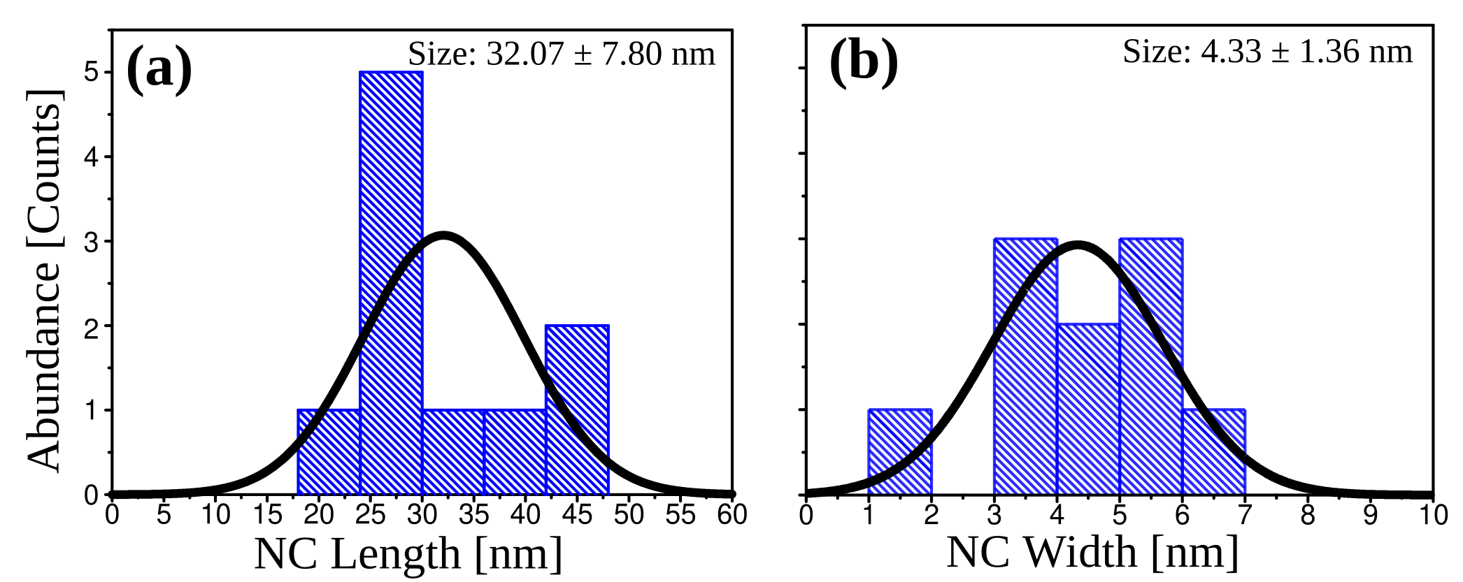
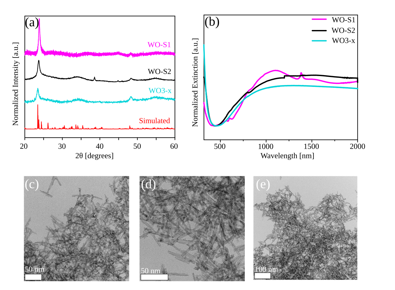
Depending on the specific W/O atomic ratio, substoichiometric tungsten (VI) oxide (WO3-x) can adopt different crystal structures, known as Magneli phases [57]. In the present study, colloidally synthezised WO3-x NCs crystallized in the monoclinic phase, as suggested by the excellent match of the experimental X-ray diffractogram (figure 3(b), blue trace) with the simulated XRD pattern (black trace) of bulk monoclinic WO2.72. The two dominant peaks in the XRD pattern of the WO3-x NCs appearing at approximately 23.5∘ and 48.3∘ can be assigned to (010) and (020) planes, respectively, suggesting the oriented growth of the NCs along the direction. This observation was confirmed by the TEM micrographs seen in figure 3(c) showing the presence of elongated NCs (nanorods) with a mean length of 32.1 7.8 nm and diameter of 4.3 1.4 nm (for further details see Supplementary Information). The inset of figure 3(c) displays a high-resolution TEM micrograph of a WO3-x nanorod having a mean lattice spacing of 3.7 Å along the direction indicated by the red lines/arrows. In undoped non-stoichiometric plasmonic metal oxides, oxygen vacancies can introduce at most two electrons per vacancy () into the crystal in order to maintain charge neutrality [58], which can subsequently lead to the reduction of nearby metal ions in the lattice (e.g., ). To investigate the electronic structure and tungsten speciation in the WO3-x nanorods, X-ray photoelectron spectroscopy (XPS) measurements were performed, the results of which were presented in our earlier report [55]. The W 4f XPS spectra suggested approximately 6% W5+ to be present in the WO3-x nanorods. In the optical extinction spectrum of the colloidal (black trace) and drop-cast (blue trace) WO3-x NCs shown in figure 4(a), a characteristic broad band starting in the visible region near 490 nm and extending into the NIR region can be observed. Based on the earlier report [55], the optical absorption in the visible region originates from intra-ionic (d-d) transitions, whereas the absorption at lower energies in the NIR region are assigned to LSPR originating from the collective oscillation of oxygen-vacancy-induced free electrons in the conduction band. The intense absorption in the UV region with an onset starting near 480 nm is assigned to the excitonic (band-to-band) transition of the semiconducting WO3-x nanorods [55].
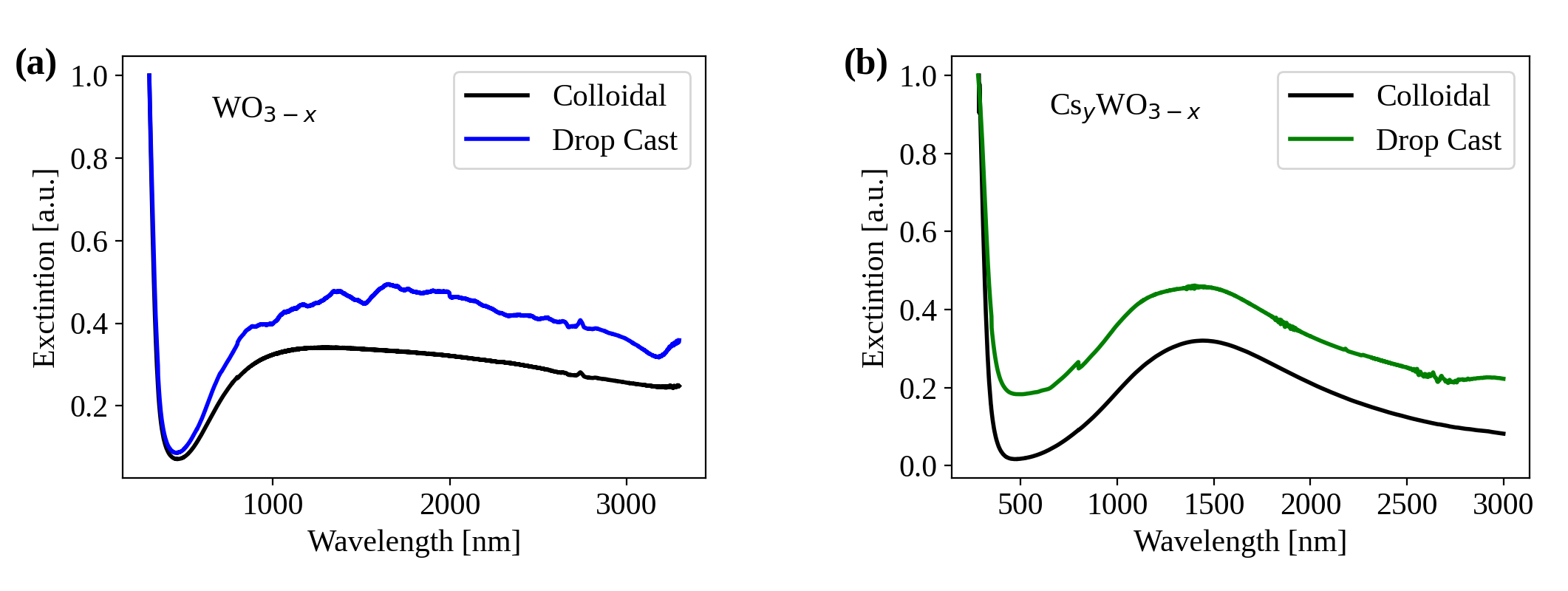
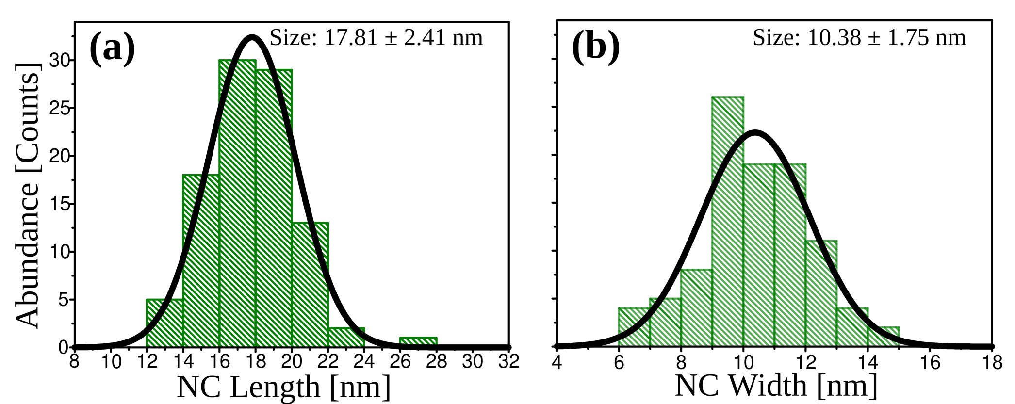
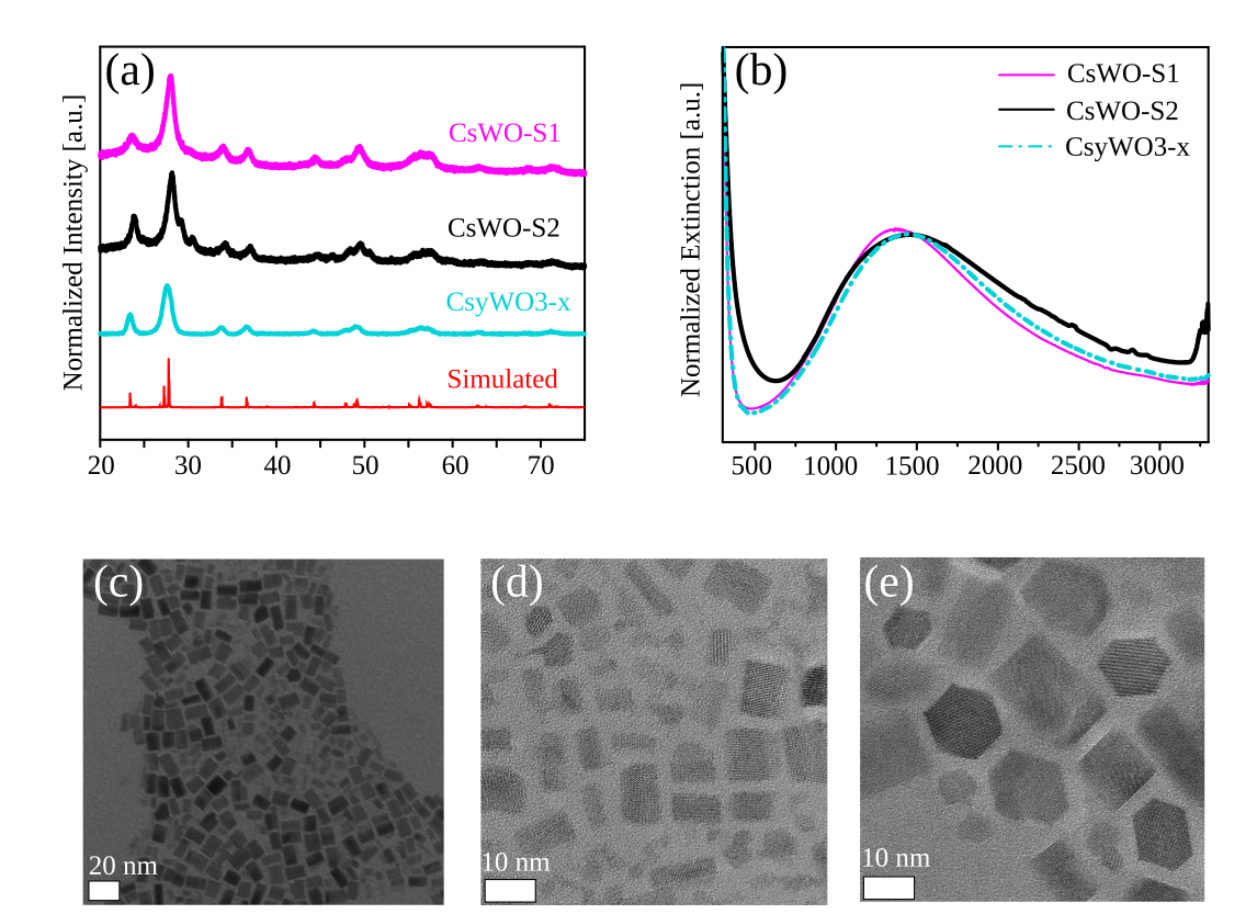
When tungsten oxide is doped with metal ions, a family of non-stoichiometric compounds of the general formula MyWO3 (M is usually an alkali metal ion) is formed, called tungsten bronzes [59]. Depending on the type and radius of the dopant ion, the crystal structure as well as the free carrier concentration, and thus the metallic conductivity, can be modulated in tungsten bronzes. The X-ray diffractogram seen in figure 3(b) reveals that as-synthesized CsyWO3-x NCs are of high purity and crystallized in the hexagonal phase, indicated by the excellent match between the experimental data and the simulated XRD pattern of the hexagonal-phase Cs0.29WO3. The two most intense peaks near 23.3∘ and 27.7∘ originate from the (002) prismatic and (200) basal planes, respectively. The TEM images shown in figure 3(d) reveal a rod-like morphology for as-synthesized CsyWO3-x NCs and a mean length and height of 17.8 nm and 10.4 nm (aspect ratio 1.7), respectively (see figure S2 of the Supplementary Information). The high-resolution TEM micrographs in figure 3(d) display an inset image of a basal plane (top) and the prismatic plane (bottom) of a CsyWO3-x NC along the direction. In tungsten bronzes the electric charge introduced by the dopant ion results in an increase in the number of free electrons in the conduction band leading to an increase in electrical conductivity. Therefore, besides the oxygen vacancies, the other source of free carriers in CsyWO3-x NCs is the cesium dopant ion. In the optical extinction spectra shown in figure 4(b), the sharply increasing UV signal originates from the bandgap absorption, similar to WO3-x NCs. The broad vis-NIR absorption band of CsyWO3-x nanorods has been reported in the literature to originate from two resonance (transverse and longitudinal) modes as a result of strong crystalline and shape anisotropy [60, 61], with an additional polaronic band in the visible region [62]. Given the geometric parameters of the as-synthesized CsyWO3-x NCs (aspect ratio 1.7), the longitudinal and transverse LSPR modes nearly overlap, resulting in the broadened single-peak absorption band seen in figure 4(b) [60, 61].
3.2 Photodetector Characterization
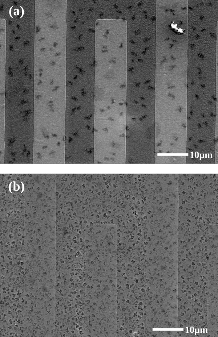
An array of 16 MSM photodetectors with varying electrode geometries was characterized using an Agilent E5262A source/measure unit probe station. The typical device resistances were measured under white light illumination () and in the dark (). Figure 5(a) shows an optical microscope image of a photodetector device with geometry similar to those used in this study. The interdigitated finger electrode structure allows colloidally suspended NCs to be readily drop-cast, as discussed previously in section 2.6.
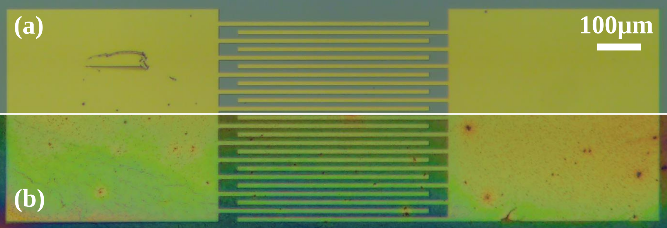
Table 1 summarizes the resistance values measured with applied bias -10 mV to +10 mV, including the mean and standard deviation values for the entire array. Two devices, referred to as A and B, showed relatively large increases in conductivity under illumination, and were selected for further measurements.
| Device | |||
|---|---|---|---|
| All | 4.24 2.44 | 0.144 0.0950 | -96.6 |
| A | 0.200 | 0.0183 | -90.8 |
| B | 4.55 | 0.181 | -96.0 |
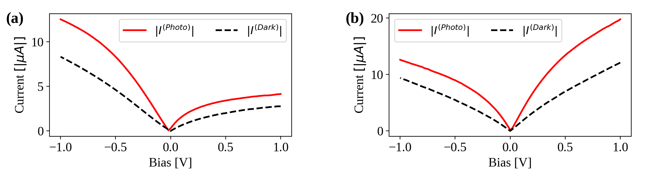
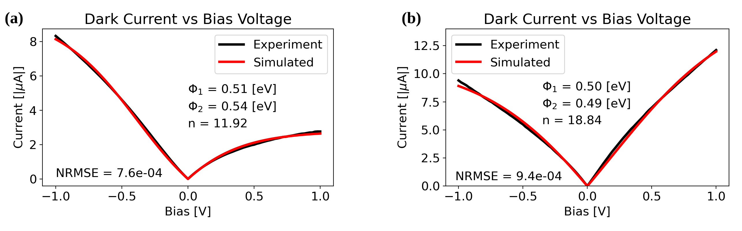
The spectral responsivities of devices A and B were measured using the setup described in figure 2. These photodetectors share the same geometry, with active area 500 m 540 m, and finger width, spacing and length of 10 m, 3 m, and 500 m, respectively. The photoresponse versus bias voltage obtained at wavelength of 1550 nm is shown in figure 6. A relatively large dark current was observed compared to similar InGaAs MSM photodetectors reported in the literature (nA [16, 13]), even with the InAlAs barrier layer present. We attribute this to a pitting surface defect density of in the InAlAs/InGaAs wafer material that lead to regions with lowered Schottky barriers and deviations from typical thermionic emission behavior [63, 64]. Using a double Schottky barrier model described in [65], the dark current through the MSM device can be modeled as
| (1) |
where , is the Schottky barrier for either contact, is the ideality factor assumed to be the same for both contacts, and are the thermionic saturation current densities for either contact. From the double Schottky barrier model, the average barrier heights between MSM contacts were estimated to be 0.53 eV and 0.50 eV for both devices A and B, compared to the theoretically expected 0.7 eV [64]. These results are also consistent with earlier theoretical predictions [16]. See the Supplementary Information for characterization of wafer morphology and details of the dark current model.
3.3 Enhancement of Photodetector Spectral Responsivity
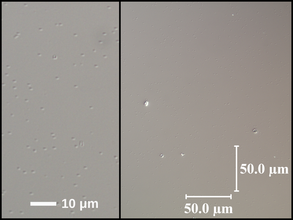
Spectral responsivity is defined as the ratio of the output photocurrent to the incident optical power, and it measures the optical-to-electrical conversion efficiency of the photodetector. The spectral responsivities of the as-fabricated photodetectors were first determined by measuring the dark current, photocurrent and power spectrum of the light source. A fixed bias voltage of -1 V was used for both devices. Note that the light source power spectrum was appropriately scaled to account for the differing areas between the photodiode detector and the MSM photodetectors, as well as variations in the beam profile. Also, measurement artifacts from switching between two gratings during the spectral sweep were removed (see Supplementary Information). Next, diluted solutions of WO3-x (100 g/L) and CsyWO3-x (152 g/L) NCs were drop-cast onto the active area of each photodetector and dried. The optical microscope image in figure 5(b) shows an example of drop-cast CsyWO3-x NCs. Similar drop-casts are obtained for WO3-x NCs, although there can be significant variability in the quality of the drop-cast (see Supplementary Information). The responsivity measurements were then repeated in order to quantify the effect of having NCs present.
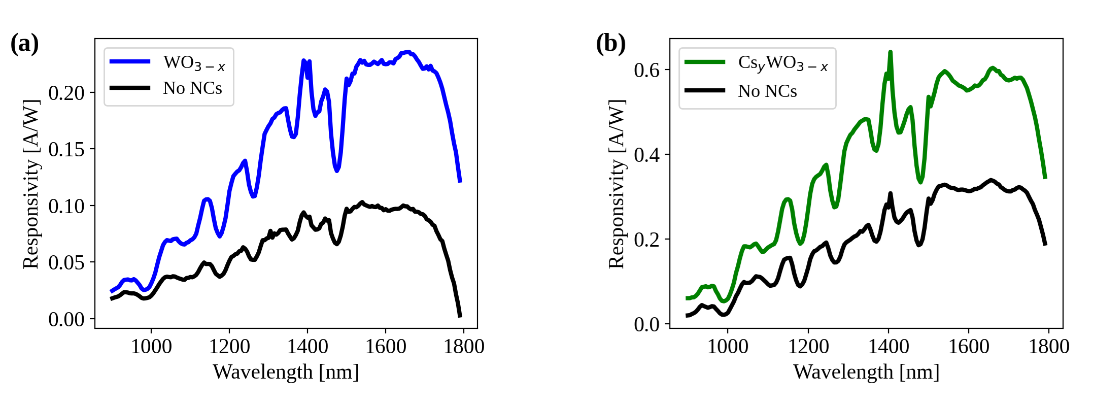
Figure 7 shows the responsivities with and without NCs for devices A and B. Device A (B) had WO3-x (CsyWO3-x) NCs drop-cast. Before NC deposition, both devices show a wavelength dependent responsivity characteristic of MSM photodetectors with an InGaAs active layer [66, 67]. Using the responsivity, the specific detectivity for both devices is calculated as:
| (2) |
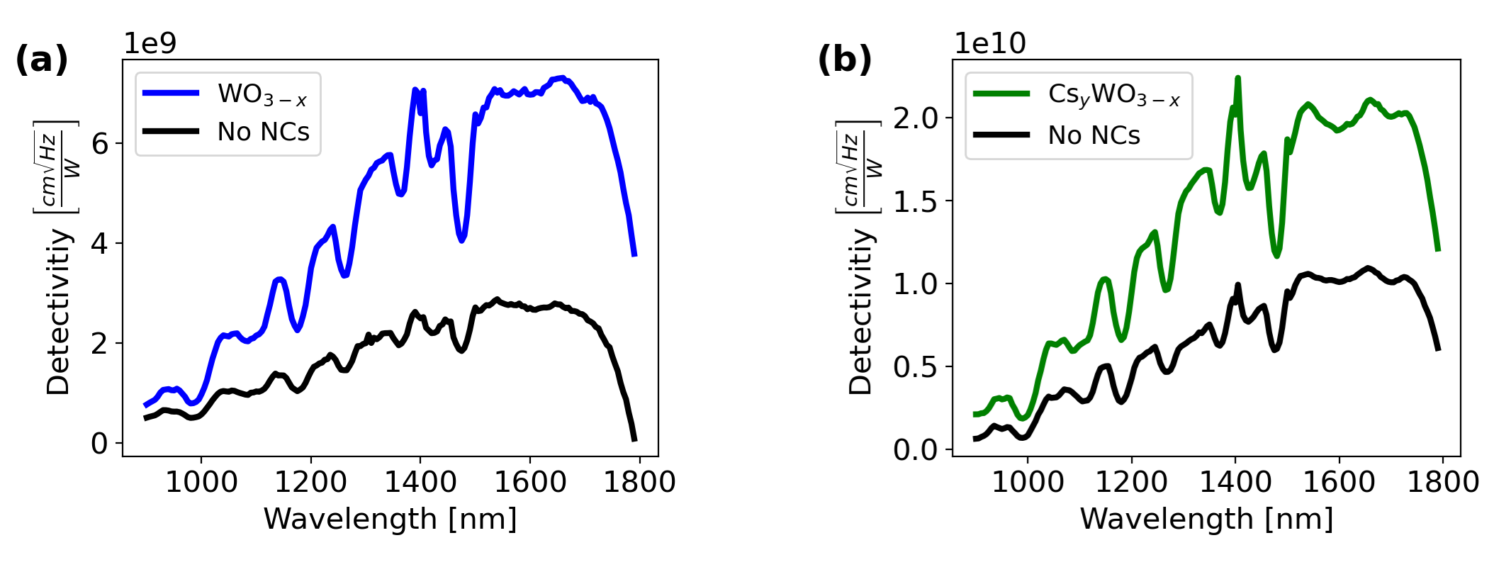
Where is the electrode contact area, is the elementary electron charge, is the average dark current, and is the wavelength-dependent responsivity. Peak detectivities of Jones and Jones are observed for devices A and B, respectively, which are comparable to other NIR photodetectors [68, 10, 29] that typically range from Jones. Furthermore, MSM InAlAs/InGaAs photodetector dectivities up to Jones can be achieved with improved substrate quality [18]. Significantly increased responsivity is observed for the addition of both WO3-x and CsyWO3-x NCs to the active regions of the photodetectors.
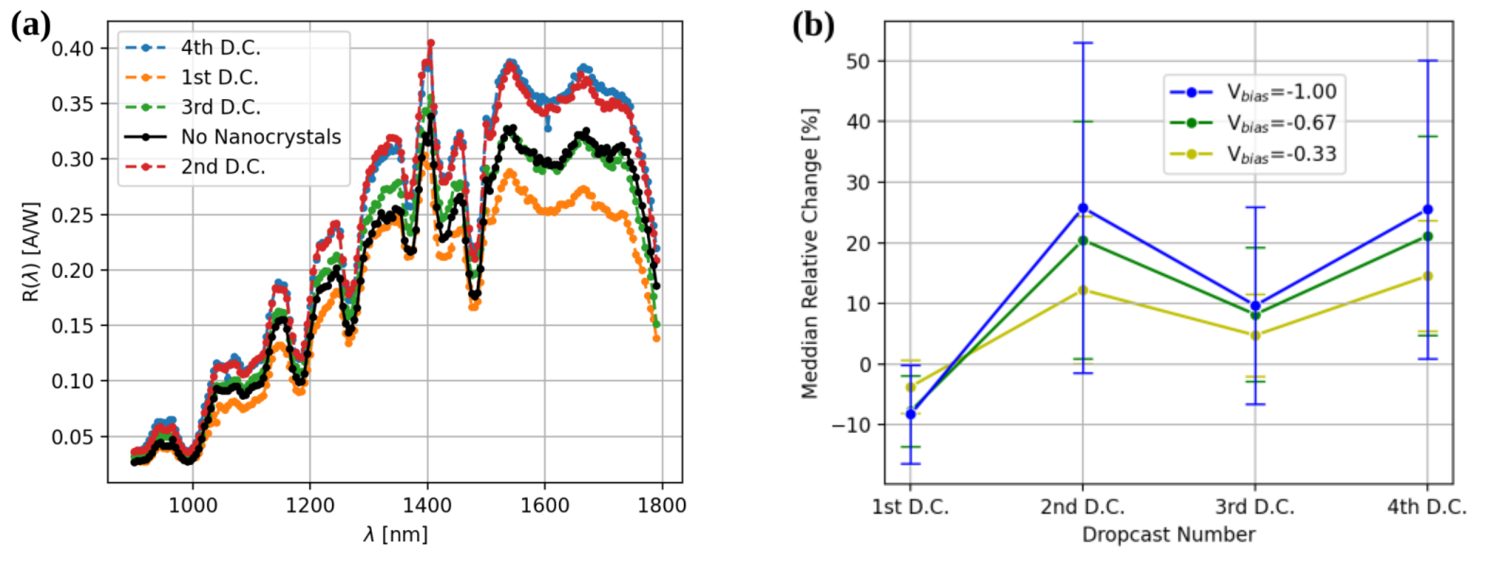
3.3.1 Relative Enhancement
It is of interest to examine the relative enhancement of responsivity as a function of wavelength and compare with the optical extinction measurements of the drop-cast NCs. The relative percent difference (RPD) is defined as:
| (3) |
where is wavelength, and and are the responsivities with and without NCs, respectively.
The RPD is plotted in figure 8, with the NC optical extinction measurements overlaid. The RPD calculated from equation 3 is in the range of 60-150% and 58-125% for devices A and B, respectively, demonstrating a strong overall enhancement of the responsivity with the addition of both NC types.
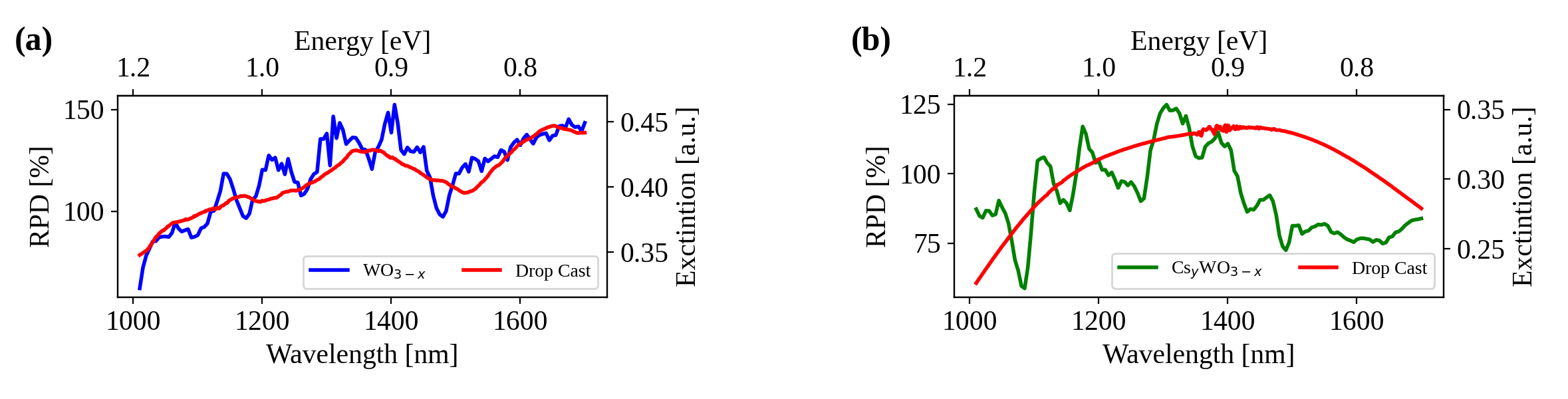
Broad agreement between the RPD and the NC extinction spectra is observed in figure 8, indicating that the plasmonic responses of the NCs likely plays a role in the enhanced photoresponse of the MSM detectors. Better agreement between the RPD and the NC extinction spectra was observed for WO3-x NCs compared to the case of CsyWO3-x NCs. The details of the spectral responses are expected to depend strongly on aggregation effects and film thickness, both of which can vary significantly between drop-casts (see Supplementary Information).
3.3.2 External Quantum Efficiency
The ability of a photodetector to convert incident photons to charges collected in the electrodes is quantified by the external quantum efficiency (EQE) as a function of wavelength [69]:
| (4) |
where is Planck’s constant and is the speed of light. Figure 9 shows the EQE for both photodetectors with and without NCs, calculated based on the data shown in figure 7. The highest EQEs are observed in the wavelength range 1400-1600 nm for both devices.
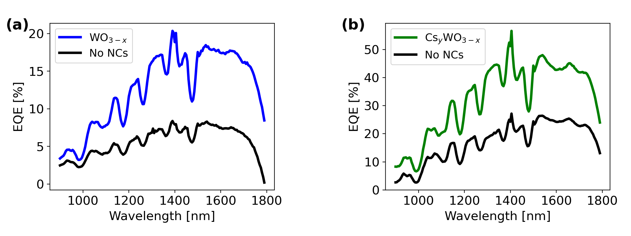
The EQE increases from approximately 7% to 20% for device A and approximately 25% to 60% for device B at a wavelength of 1400 nm, indicating that 2-3 times as many charge carriers are generated or collected after the addition of the WO3-x and CsyWO3-x NCs. The EQEs before the addition of NCs are comparable to those reported for other NIR photodetectors [70] and are enhanced by the addition of NCs.
4 Discussion
Mechanisms for plasmonic response giving rise to increased photodetector EQEs have been debated in recent years. Possible mechanisms to explain our observations include:
- 1.
- 2.
- 3.
It is not clear from the present data which of these mechanisms are present or dominant in our devices. However, recent work has demonstrated that injection of plasmonically-excited carriers can play a primary role in enhanced photodetection [29, 70]. Evidence that hot carrier injection is the primary mechanism for WO3-x nanorod photodetectors has been demonstrated [44]. The plasmonic absorption band for our NCs ranges over 0.7-1.2 eV. Depending on the work function of the NCs, a Schottky barrier could form that would be low enough to inject energetic carriers into the bulk semiconductor, generating a photocurrent under an applied bias. To test this hypothesis, carrier injection could be suppressed by depositing a thin, wide-bandgap insulating layer between the NCs and the InAlAs surface. The influence of hot carrier injection on photodetector responsivity could be studied by varying the doping concentration of the NCs, where a higher doping concentration would be expected to yield a stronger increase in responsivity. Additionally, LSPR-generated EM fields can be orders of magnitude stronger than the incident field. A stronger EM field in the InGaAs active layer would generate electron-hole pairs at a higher rate. Here, the enhancement in photodetection would be governed by the thickness of the InAlAs buffer layer, since the electric field generated at the NC surface drops off as [71]. This mechanism can be tested by varying the thickness of the InAlAs layer.
The magnitude and distribution of the EM field is determined by the NC morphology which governs the packing behavior of the NCs and the dominant LSPR mode [61]. The optimal morphology for increased density of EM field hot spots in the active region could be investigated using finite-difference time-domain EM simulations [61, 60], and correlated with responsivity measurements for different NC morphologies.
Finally, enhancement in EQE from the NCs acting as an AR coating could be potentially challenging to separate from other LSPR effects. Plasmonic nanostructures have been used for AR coatings [78], alongside commonly used dielectric nanoparticles. A systematic study of the reflectivity of transition metal oxide NC films on various surfaces could clarify the significance of this effect.
Future work will aim to clarify the dominant mechanisms for enhancement and improve performance through the following approaches:
-
1.
Synthesizing CsyWO3-x NCs with varied aspect ratios and carrier concentrations to elucidate the role of LSPR;
-
2.
Characterizing performance improvements using non-plasmonic dielectric AR coatings;
-
3.
Improving sensitivity by using higher-quality substrates for MBE growth to reduce dark current. In addition, incorporating control devices with variable-thickness dielectric barriers between the NCs and the InAlAs surface to test the hot carrier injection hypothesis;
-
4.
Applying NCs via cold vacuum aerosol deposition, or spin coating with NCs embedded in a silica matrix, in order to improve the reproducibility and quality of NC coverage.
5 Conclusion
In this study we have demonstrated that easy-to-fabricate MSM photodetectors can exhibit improved performance in the NIR with the addition of semiconducting WO3-x or CsyWO3-x NCs to the active area. This shows the potential of both non-stoichiometric and doped transition metal oxide plasmonic nanomaterials for various IR optoelectronics applications, such as enhanced speed and sensitivity of receivers in optical fiber communications or increased range and reliability of Light Detection and Ranging (LiDAR) systems for autonomous vehicles. The ease of deposition by drop-casting is convenient for rapid prototyping of modified MSM detectors, but lacks the consistency needed for industrial scaling.
In future work, the mechanisms for plasmonic enhancement of photodetection can be distinguished by systematic experiments, as previously discussed, along with comparison to finite-difference time-domain EM simulations. Other directions for improvement include the use of higher quality substrates for MBE growth (reduced dark current), the use of more sophisticated NC deposition methods for reproducibility and consistency, and the use of a transparent conductive material (such as indium tin oxide) for the electrodes.
Acknowledgments
This research was undertaken thanks in part to funding from the Canada First Research Excellence Fund (Transformative Quantum Technologies) and the Natural Sciences and Engineering Research Council (NSERC) of Canada. The University of Waterloo’s QNFCF Facility was used for this work. This infrastructure would not be possible without the significant contributions of CFREF-TQT, CFI, ISED, the Ontario Ministry of Research and Innovation, and Mike and Ophelia Lazaridis. Their support is gratefully acknowledged.
Author contributions
ZDM performed the experimental work characterizing photodetectors and NC solutions for drop casting, data analysis and plotting, and led the writing of the manuscript. GyJ synthesized and characterized NC samples and contributed to writing the manuscript. AJ fabricated the photodetectors. HW grew the InGaAs wafer. JB and PVR supervised the project and contributed to writing the manuscript. All authors reviewed the manuscript.
Data availability statement
The data that support the findings of this study are available upon request from the authors.
ORCID iDs
Zach D. Merino https://orcid.org/0000-0001-6224-800X
Gyorgy Jaics https://orcid.org/0009-0007-6210-4736
Pavle V. Radovanovic https://orcid.org/0000-0002-4151-6746
Jonathan Baugh https://orcid.org/0000-0002-9300-7134
References
References
- [1] A. Rogalski, J. Antoszewski, and L. Faraone, “Third-generation infrared photodetector arrays,” Journal of Applied Physics, vol. 105, May 2009.
- [2] P. Martyniuk, J. Antoszewski, M. Martyniuk, L. Faraone, and A. Rogalski, “New concepts in infrared photodetector designs,” Applied Physics Reviews, vol. 1, p. 041102, Dec. 2014.
- [3] S. D. Gunapala, S. V. Bandara, J. K. Liu, J. M. Mumolo, S. B. Rafol, D. Z. Ting, A. Soibel, and C. Hill, “Quantum well infrared photodetector technology and applications,” IEEE Journal of Selected Topics in Quantum Electronics, vol. 20, pp. 154–165, Nov. 2014.
- [4] Z.-M. Zhong, F. Peng, L. Ying, Z.-Q. Huang, W.-K. Zhong, G. Yu, Y. Cao, and F. Huang, “Infrared photodetectors and image arrays made with organic semiconductors,” Chinese Journal of Polymer Science, vol. 41, pp. 1629–1637, Apr. 2023.
- [5] Y. Zhu, H. Chen, R. Han, H. Qin, Z. Yao, H. Liu, Y. Ma, X. Wan, G. Li, and Y. Chen, “High-speed flexible near-infrared organic photodiode for optical communication,” National Science Review, vol. 11, Dec. 2023.
- [6] F. Zhuge, Z. Zheng, P. Luo, L. Lv, Y. Huang, H. Li, and T. Zhai, “Nanostructured materials and architectures for advanced infrared photodetection,” Advanced Materials Technologies, vol. 2, May 2017.
- [7] Z. Li, Z. He, C. Xi, F. Zhang, L. Huang, Y. Yu, H. H. Tan, C. Jagadish, and L. Fu, “Review on iii–v semiconductor nanowire array infrared photodetectors,” Advanced Materials Technologies, vol. 8, Apr. 2023.
- [8] K. Ramakrishnan, B. Ajitha, and Y. Ashok Kumar Reddy, “Review on metal sulfide-based nanostructures for photodetectors: From ultraviolet to infrared regions,” Sensors and Actuators A: Physical, vol. 349, p. 114051, Jan. 2023.
- [9] L. Wang, B. Wang, Y. Zhang, L. Meng, H. Sun, T. Liu, N. Zhang, Z. Jiang, and H. Hu, “Infrared broadband enhancement of responsivity in ge photodetectors decorated with au nanoparticles,” Optics Express, vol. 29, p. 12941, Apr. 2021.
- [10] S. Bansal, “Long-wave bilayer graphene/hgcdte based gbp type-ii superlattice unipolar barrier infrared detector,” Results in Optics, vol. 12, p. 100425, July 2023.
- [11] J. Brouckaert, G. Roelkens, D. Van Thourhout, and R. Baets, “Compact inalas–ingaas metal– semiconductor– metal photodetectors integrated on silicon-on-insulator waveguides,” IEEE Photonics Technology Letters, vol. 19, pp. 1484–1486, Oct. 2007.
- [12] D. H. Unal and I. Demir, “Ingaas-based msm photodetector: Researching absorption layer, barrier layer, and digital graded superlattice layer with 3d simulation,” Results in Optics, vol. 13, p. 100581, Dec. 2023.
- [13] J. Soole and H. Schumacher, “Ingaas metal-semiconductor-metal photodetectors for long wavelength optical communications,” IEEE Journal of Quantum Electronics, vol. 27, pp. 737–752, Mar. 1991.
- [14] D. Kuhl, F. Hieronymi, E. Bottcher, T. Wolf, D. Bimberg, J. Kuhl, and M. Klingenstein, “Influence of space charges on the impulse response of ingaas metal-semiconductor-metal photodetectors,” Journal of Lightwave Technology, vol. 10, pp. 753–759, June 1992.
- [15] A. Salem and K. Brennan, “Theoretical study of the response of ingaas metal-semiconductor-metal photodetectors,” IEEE Journal of Quantum Electronics, vol. 31, pp. 944–953, May 1995.
- [16] W. A. Wohlmuth, M. Arafa, A. Mahajan, P. Fay, and I. Adesida, “Ingaas metal-semiconductor-metal photodetectors with engineered schottky barrier heights,” Applied Physics Letters, vol. 69, pp. 3578–3580, Dec. 1996.
- [17] K. Aliberti, M. Wraback, M. Stead, P. Newman, and H. Shen, “Measurements of ingaas metal–semiconductor–metal photodetectors under high-illumination conditions,” Applied Physics Letters, vol. 80, pp. 2848–2850, Apr. 2002.
- [18] J. Kim, W. Johnson, S. Kanakaraju, L. Calhoun, and C. Lee, “Improvement of dark current using inp/ingaasp transition layer in large-area ingaas msm photodetectors,” IEEE Transactions on Electron Devices, vol. 51, pp. 351–356, Mar. 2004.
- [19] B. Smiri, M. Ben Arbia, D. Ilkay, F. Saidi, Z. Othmen, B. Dkhil, A. Ismail, E. Sezai, F. Hassen, and H. Maaref, “Optical and structural properties of in-rich inxga1-xas epitaxial layers on (1 0 0) inp for swir detectors,” Materials Science and Engineering: B, vol. 262, p. 114769, Dec. 2020.
- [20] P. Berini, “Surface plasmon photodetectors and their applications,” Laser amp; Photonics Reviews, vol. 8, pp. 197–220, June 2013.
- [21] A. Dorodnyy, Y. Salamin, P. Ma, J. Vukajlovic Plestina, N. Lassaline, D. Mikulik, P. Romero-Gomez, A. Fontcuberta i Morral, and J. Leuthold, “Plasmonic photodetectors,” IEEE Journal of Selected Topics in Quantum Electronics, vol. 24, pp. 1–13, Nov. 2018.
- [22] J. Zhang, Y. Wang, D. Li, Y. Sun, and L. Jiang, “Engineering surface plasmons in metal/nonmetal structures for highly desirable plasmonic photodetectors,” ACS Materials Letters, vol. 4, pp. 343–355, Jan. 2022.
- [23] S. Butun, N. A. Cinel, and E. Ozbay, “Lspr enhanced msm uv photodetectors,” Nanotechnology, vol. 23, p. 444010, Oct. 2012.
- [24] K. M. Azizur-Rahman and R. R. LaPierre, “Optical design of a mid-wavelength infrared insb nanowire photodetector,” Nanotechnology, vol. 27, p. 315202, June 2016.
- [25] C. J. Goosney, V. M. Jarvis, D. P. Wilson, N. I. Goktas, and R. R. LaPierre, “Insb nanowires for multispectral infrared detection,” Semiconductor Science and Technology, vol. 34, p. 035023, Feb. 2019.
- [26] T. Yang, S. Hertenberger, S. Morkötter, G. Abstreiter, and G. Koblmüller, “Size, composition, and doping effects on in(ga)as nanowire/si tunnel diodes probed by conductive atomic force microscopy,” Applied Physics Letters, vol. 101, Dec. 2012.
- [27] Y. Zhu, H. Xu, P. Yu, and Z. Wang, “Engineering plasmonic hot carrier dynamics toward efficient photodetection,” Applied Physics Reviews, vol. 8, Apr. 2021.
- [28] N. Yan, Y. Qiu, X. He, X. Tang, Q. Hao, and M. Chen, “Plasmonic enhanced nanocrystal infrared photodetectors,” Materials, vol. 16, p. 3216, Apr. 2023.
- [29] W.-Y. Lee, J. Lee, H.-J. Kwon, K. Kim, H. Kang, and J. Jang, “High-detectivity silver telluride nanoparticle-based near-infrared photodetectors functionalized with surface-plasmonic gold nanoparticles,” Applied Surface Science, vol. 654, p. 159563, May 2024.
- [30] S. K. Cushing and N. Wu, “Plasmon-enhanced solar energy harvesting,” Interface magazine, vol. 22, pp. 63–67, Jan. 2013.
- [31] J. Huang and L. Luo, “Low‐dimensional plasmonic photodetectors: Recent progress and future opportunities,” Advanced Optical Materials, vol. 6, Feb. 2018.
- [32] Y. Ji, W. Xu, D. Li, D. Zhou, X. Chen, N. Ding, J. Li, N. Wang, X. Bai, and H. Song, “Semiconductor plasmon enhanced monolayer upconversion nanoparticles for high performance narrowband near-infrared photodetection,” Nano Energy, vol. 61, pp. 211–220, July 2019.
- [33] J. Li, Z. Lou, and B. Li, “Engineering plasmonic semiconductors for enhanced photocatalysis,” Journal of Materials Chemistry A, vol. 9, no. 35, pp. 18818–18835, 2021.
- [34] A. A. Alqanoo, N. M. Ahmed, M. Hashim, M. A. Almessiere, S. A. Taya, and S. H. Zyoud, “Silver nanowires assisted porous silicon for high photodetector sensitivity using surface plasmonic phenomena,” Sensors and Actuators A: Physical, vol. 347, p. 113942, Nov. 2022.
- [35] R. Rajkumari, C. Ngangbam, and N. K. Singh, “High detectivity photodetector based on wo3 nanowires by the surface plasmonic effect of ag nanoparticles,” IEEE Electron Device Letters, vol. 43, pp. 470–473, Mar. 2022.
- [36] L. Zheng, Y. Yang, C. R. Bowen, L. Jiang, Z. Shu, Y. He, H. Yang, Z. Xie, T. Lu, F. Hu, and W. Yang, “A high-performance uv photodetector with superior responsivity enabled by a synergistic photo/thermal enhancement of localized surface plasmon resonance,” Journal of Materials Chemistry C, vol. 11, no. 18, pp. 6227–6238, 2023.
- [37] S. Maity, K. Sarkar, and P. Kumar, “Wo3-np-activated ws2 layered heterostructures for efficient broadband (254 nm–940 nm) photodetection,” Nanoscale, vol. 15, no. 39, pp. 16068–16079, 2023.
- [38] Y. Liu, R. Cheng, L. Liao, H. Zhou, J. Bai, G. Liu, L. Liu, Y. Huang, and X. Duan, “Plasmon resonance enhanced multicolour photodetection by graphene,” Nature Communications, vol. 2, Dec. 2011.
- [39] Y. Wu, X.-J. Sun, Y.-P. Jia, and D.-B. Li, “Review of improved spectral response of ultraviolet photodetectors by surface plasmon,” Chinese Physics B, vol. 27, p. 126101, Dec. 2018.
- [40] C. Tian, D. Jiang, B. Li, J. Lin, Y. Zhao, W. Yuan, J. Zhao, Q. Liang, S. Gao, J. Hou, and J. Qin, “Performance enhancement of zno uv photodetectors by surface plasmons,” ACS Applied Materials amp; Interfaces, vol. 6, pp. 2162–2166, Jan. 2014.
- [41] S. Kunwar, S. Pandit, J.-H. Jeong, and J. Lee, “Improved photoresponse of uv photodetectors by the incorporation of plasmonic nanoparticles on gan through the resonant coupling of localized surface plasmon resonance,” Nano-Micro Letters, vol. 12, Apr. 2020.
- [42] P. Senanayake, C.-H. Hung, J. Shapiro, A. Lin, B. Liang, B. S. Williams, and D. L. Huffaker, “Surface plasmon-enhanced nanopillar photodetectors,” Nano Letters, vol. 11, pp. 5279–5283, Nov. 2011.
- [43] K.-T. Lin, H. Lin, and B. Jia, “Plasmonic nanostructures in photodetection, energy conversion and beyond,” Nanophotonics, vol. 9, pp. 3135–3163, June 2020.
- [44] Y. Zhu, W. Lu, T. Gu, X. Gao, N. Yu, S. Y. Ketkov, and Z. Zhang, “W18o49 nanowire arrays for plasmonic photodetector with electromediated broadband photoresponse,” ACS Applied Nano Materials, vol. 6, pp. 11104–11114, June 2023.
- [45] L. Daugas, K. Lahlil, C. C. de Langavant, I. Florea, E. Larquet, H. Henry, J. Kim, and T. Gacoin, “Investigation of lspr coupling effects toward the rational design of csxwo3– based solar nir filtering coatings,” Advanced Functional Materials, vol. 33, June 2023.
- [46] T. Nütz, U. z. Felde, and M. Haase, “Wet-chemical synthesis of doped nanoparticles: Blue-colored colloids of n-doped sno2:sb,” The Journal of Chemical Physics, vol. 110, pp. 12142–12150, June 1999.
- [47] T. Wang and P. V. Radovanovic, “Free electron concentration in colloidal indium tin oxide nanocrystals determined by their size and structure,” The Journal of Physical Chemistry C, vol. 115, pp. 406–413, Dec. 2010.
- [48] J. M. Luther, P. K. Jain, T. Ewers, and A. P. Alivisatos, “Localized surface plasmon resonances arising from free carriers in doped quantum dots,” Nature Materials, vol. 10, pp. 361–366, Apr. 2011.
- [49] E. Della Gaspera, A. S. R. Chesman, J. van Embden, and J. J. Jasieniak, “Non-injection synthesis of doped zinc oxide plasmonic nanocrystals,” ACS Nano, vol. 8, pp. 9154–9163, Aug. 2014.
- [50] X. Dai, M. Tchernycheva, and C. Soci, Compound Semiconductor Nanowire Photodetectors, pp. 75–107. Elsevier, 2016.
- [51] H. Fang, M. Hegde, P. Yin, and P. V. Radovanovic, “Tuning plasmon resonance of in2o3 nanocrystals throughout the mid-infrared region by competition between electron activation and trapping,” Chemistry of Materials, vol. 29, pp. 4970–4979, May 2017.
- [52] A. Ahmadivand, M. Karabiyik, and N. Pala, Plasmonic photodetectors, pp. 157–193. Elsevier, 2016.
- [53] G. Bao, D. Li, X. Sun, M. Jiang, Z. Li, H. Song, H. Jiang, Y. Chen, G. Miao, and Z. Zhang, “Enhanced spectral response of an algan-based solar-blind ultraviolet photodetector with al nanoparticles,” Optics Express, vol. 22, p. 24286, Sept. 2014.
- [54] P. K. Sahoo, S. Kalyan Kamal, M. Premkumar, T. Jagadeesh Kumar, B. Sreedhar, A. Singh, S. Srivastava, and K. Chandra Sekhar, “Synthesis of tungsten nanoparticles by solvothermal decomposition of tungsten hexacarbonyl,” International Journal of Refractory Metals and Hard Materials, vol. 27, pp. 784–791, July 2009.
- [55] A. Kenny-Wilby, G. Jaics, C. Zhang, P. Yin, and P. V. Radovanovic, “Revisiting plasmonic properties of complex semiconductor nanocrystals using magnetic circular dichroism spectroscopy: A cautionary tale,” The Journal of Physical Chemistry C, vol. 127, pp. 1087–1096, Jan. 2023.
- [56] T. M. Mattox, A. Bergerud, A. Agrawal, and D. J. Milliron, “Influence of shape on the surface plasmon resonance of tungsten bronze nanocrystals,” Chemistry of Materials, vol. 26, pp. 1779–1784, Feb. 2014.
- [57] D. B. Migas, V. L. Shaposhnikov, and V. E. Borisenko, “Tungsten oxides. ii. the metallic nature of magnéli phases,” Journal of Applied Physics, vol. 108, Nov. 2010.
- [58] S. D. Lounis, E. L. Runnerstrom, A. Llordés, and D. J. Milliron, “Defect chemistry and plasmon physics of colloidal metal oxide nanocrystals,” The Journal of Physical Chemistry Letters, vol. 5, pp. 1564–1574, Apr. 2014.
- [59] L. E. Conroy and M. J. Sienko, “Magnetic susceptibility of the lithium tungsten bronzes,” Journal of the American Chemical Society, vol. 74, no. 14, pp. 3520–3522, 1952.
- [60] Y. Cheref, F. Lochon, L. Daugas, C. Cleret de Langavant, E. Larquet, A. Baron, T. Gacoin, and J. Kim, “Dual-band lspr of tungsten bronze nanocrystals tunable over nir and swir ranges,” Chemistry of Materials, vol. 34, pp. 9795–9802, Oct. 2022.
- [61] J. Kim, A. Agrawal, F. Krieg, A. Bergerud, and D. J. Milliron, “The interplay of shape and crystalline anisotropies in plasmonic semiconductor nanocrystals,” Nano Letters, vol. 16, pp. 3879–3884, May 2016.
- [62] K. Machida, M. Okada, and K. Adachi, “Excitations of free and localized electrons at nearby energies in reduced cesium tungsten bronze nanocrystals,” Journal of Applied Physics, vol. 125, Mar. 2019.
- [63] O. Breitenstein, P. Altermatt, K. Ramspeck, M. Green, J. Zhao, and A. Schenk, “Interpretation of the commonly observed i-v characteristics of c-si cells having ideality factor larger than two,” in 2006 IEEE 4th World Conference on Photovoltaic Energy Conference, IEEE, 2006.
- [64] I. B. Chistokhin, M. S. Aksenov, N. Valisheva, D. V. Dmitriev, I. V. Marchishin, A. I. Toropov, and K. S. Zhuravlev, “The influence of the inalas layer surface morphology on the temperature dependence of parameters of au/ti/n-inalas(001) schottky diodes,” Technical Physics Letters, vol. 45, pp. 180–184, Feb. 2019.
- [65] G. Bhattacharya and A. Venimadhav, “An alternative approach to extract diode parameters from metal–semiconductor–metal asymmetric schottky diodes,” Journal of Physics D: Applied Physics, vol. 55, p. 435101, Aug. 2022.
- [66] J. Chen, J. Wang, X. Li, J. Chen, F. Yu, J. He, J. Wang, Z. Zhao, G. Li, X. Chen, and W. Lu, “Recent progress in improving the performance of infrared photodetectors via optical field manipulations,” Sensors, vol. 22, p. 677, Jan. 2022.
- [67] X. Li, J. Zhang, C. Yue, X. Tang, Z. Gao, Y. Jiang, C. Du, Z. Deng, H. Jia, W. Wang, and H. Chen, “High performance visible-swir flexible photodetector based on large-area ingaas/inp pin structure,” Scientific Reports, vol. 12, May 2022.
- [68] S. Bansal, K. Prakash, K. Sharma, N. Sardana, S. Kumar, N. Gupta, and A. K. Singh, “A highly efficient bilayer graphene/zno/silicon nanowire based heterojunction photodetector with broadband spectral response,” Nanotechnology, vol. 31, p. 405205, July 2020.
- [69] L. Shi, K. Chen, A. Zhai, G. Li, M. Fan, Y. Hao, F. Zhu, H. Zhang, and Y. Cui, “Status and outlook of metal–inorganic semiconductor–metal photodetectors,” Laser amp; Photonics Reviews, vol. 15, Dec. 2020.
- [70] R. Duan, W. Qi, P. Li, K. Tang, G. Ru, and W. Liu, “A high-performance mos 2 -based visible–near-infrared photodetector from gateless photogating effect induced by nickel nanoparticles,” Research, vol. 6, Jan. 2023.
- [71] I. Abdulhalim, “Coupling configurations between extended surface electromagnetic waves and localized surface plasmons for ultrahigh field enhancement,” Nanophotonics, vol. 7, pp. 1891–1916, Nov. 2018.
- [72] Y. Tian and T. Tatsuma, “Mechanisms and applications of plasmon-induced charge separation at tio2 films loaded with gold nanoparticles,” Journal of the American Chemical Society, vol. 127, pp. 7632–7637, Apr. 2005.
- [73] L. Chu, C. Xu, D. Liu, C. Nie, and L. Deng, “Plasmon-induced hot-electron injection effect: mechanism of performance enhancement for zno msm hybrid photodetector by introducing ag nws and mxene,” Journal of Physics D: Applied Physics, vol. 57, p. 045102, Oct. 2023.
- [74] C. Clavero, “Plasmon-induced hot-electron generation at nanoparticle/metal-oxide interfaces for photovoltaic and photocatalytic devices,” Nature Photonics, vol. 8, pp. 95–103, Jan. 2014.
- [75] J. Luo, Q. Wu, L. Zhou, W. Lu, W. Yang, and J. Zhu, “Plasmon-induced hot carrier dynamics and utilization,” Photonics Insights, vol. 2, no. 4, p. R08, 2023.
- [76] K. Katagiri, S.-i. Yamazaki, K. Inumaru, and K. Koumoto, “Anti-reflective coatings prepared via layer-by-layer assembly of mesoporous silica nanoparticles and polyelectrolytes,” Polymer Journal, vol. 47, pp. 190–194, Nov. 2014.
- [77] S. Zeb, G. Sun, Y. Nie, H. Xu, Y. Cui, and X. Jiang, “Advanced developments in nonstoichiometric tungsten oxides for electrochromic applications,” Materials Advances, vol. 2, no. 21, pp. 6839–6884, 2021.
- [78] B. Singh, M. M. Shabat, and D. M. Schaadt, “Large photocurrent density enhancement assisted by non-absorbing spherical dielectric nanoparticles in a gaas layer,” Scientific Reports, vol. 10, Oct. 2020.
6 Supplementary Information
6.1 Supplement A: Nanocrystal (NC) Characterization
Figures 10 and 11 provide information on the size and shape distributions of the WO3-x and CsyWO3-x NCs, as determined from TEM images. Figure 12 shows energy dispersive X-ray spectroscopy results that were used to determine the composition of the CsyWO3-x NCs. Figures 13 and 14 show the crystalline and optical characterization for WO3-x and CsyWO3-x NCs, respectively. Tables 2 and 3 present a summary of these results.
| Sample |
UV-NIR
Max [nm] |
XRD
(010) |
XRD
(020) |
|---|---|---|---|
| WO3-x | 1126 | 23.4-0.5 | 48.3-0.8 |
| WO-S1 | 1098 | 23.8-0.5 | 48.3-0.6 |
| WO-S2 | 1153 | 23.7-0.7 | 48.3-1.3 |
| Sample | AR |
UV-NIR
Max [nm] |
XRD
(002) |
XRD
(200) |
XRD
(112) |
XRD
(202) |
| CsyWO3-x | 1.6 | 1442 | 23.4-0.8 | 27.7-1.3 | 33.8-0.8 | 36.7-0.9 |
| CsWO-S1 | 1.5 | 1363 | 23.6-0.8 | 28.0-1.4 | 34.2-0.9 | 37.0-0.8 |
| CsWO-S2 | 1.6 | 1449 | 23.8-0.8 | 28.1-1.3 | 33.9-1.0 | 36.9-0.9 |
6.2 Supplement B: Light Source Characterization
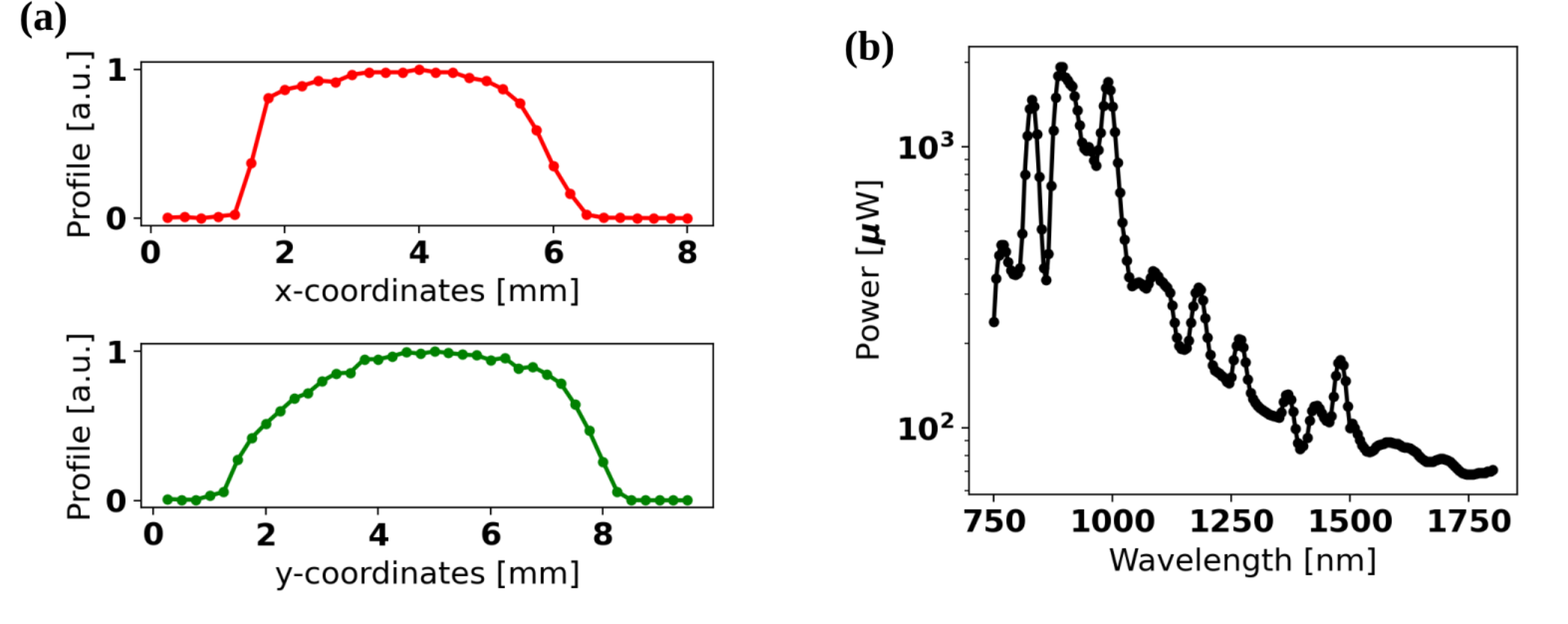
Cross-sections of the beam profile are shown attached to a head on image of the beam at 550 nm wavelength light. The image of the beam is not to scale with the cross-sectional beam profiles. The beam profiles were measured using a standard knife-edge measurement.
6.3 Supplement C: Spectral Responsivity Normalization and Incident Power
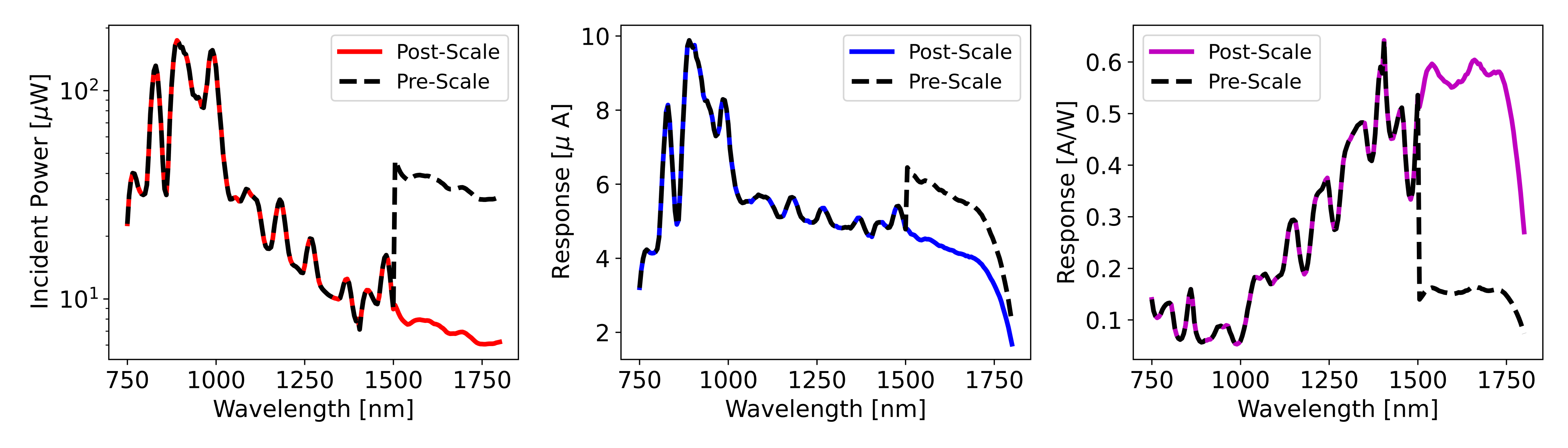
The total integrated power, , incident on a power sensor photodiode area is recorded over a band of wavelengths. From the beam profile measurements above, the photodetector was positioned in a region of the beam profile with maximal power density, . For the typical photodetector active area, the power density is nearly constant across the device. Calculating the total power incident on the photodetector, , is performed by numerical integration of along cross sections over the dimensions of the device active area position relative to the beam profile. The was calculated from a beam profile measurement taken at a wavelength of 550 nm. Assuming the beam profile does not vary with wavelength, was calculated as the normalized total integrated power:
| (5) |
This method is a reasonable lower bound approximation for the incident power seen by the photodetectors. Since refractive optics were used for beam collimation and focusing, the beam spot size will slightly increase for due to chromatic aberrations, decreasing the power density.
Measuring the photodetector current or the light source power spectrum yields discontinuities in the measured spectra due to the change of diffraction grating at a wavelength of 1500 nm. The power density at the focal plane of the photodetectors changes due to power transmission variation between the two diffraction gratings used to perform each wavelength sweep measurement. The discontinuity is removed by properly normalizing the current and power spectra for the wavelength range associated with one of the diffraction gratings. The wavelength range which is normalized is 1500-1800 nm and the spectra are normalized by or defined as:
| (6) |
where G1/G2 refer to diffraction blaze gratings (G1 grating 1, G2 grating 2) utilized for and which represent the measured quantities: (current ) or (power ). The normalized response is then calculating using the scale factors and :
| (7) |
where , , and represents the union of two data sets collected from measurements.
The power and photocurrent measurements are scaled independently such that the last/first values in the wavelength ranges 750-1500 nm and 1505-1800 nm are equivalent for both power and photocurrent spectra. The pre- and post-scaled spectra are plotted in figure 16 where the dashed lines are the pre-scaled portions of the respective spectra.
6.4 Supplement D: In0.52Al0.48As/In0.53Ga0.47As Wafer Morphology
As stated in the main text, we observed larger than expected dark currents in the MSM photodetectors, despite having an In0.52Al0.48As barrier layer present. From Nomarski microscope images (see figure S6) of the InAlAs surface, pitting defects can be observed with a density of 106cm-2. Such defects can provide low resistance pathways between the metal electrodes and InGaAs active layer. Based on previous MBE growths in the same system, we suspect that these defects originate from defects native to the InP growth wafer.
6.5 Supplement E: Schottky Contact Model
Using a thermonic emission model for a double Schottky diode from [65], the dark current through the device is given by:
where
and where , is the Schottky barrier for either contact, is the ideality factor assumed to be the same for both contacts, is the area of the contact, A m-2 K-2 is the Richardson constant for InAlAs, and are the thermionic saturation current densities for either contact. From fitting our dark current data to this model, the Schottky barriers and ideality factor are estimated to be: (device A) eV, eV, and (device B) eV, eV, and . The theoretically expected Shottky barrier for Ti/InAlAs is 0.7 eV [65]. Figure 18 shows each model fit and the experimental dark current data with the Normalized Root Mean Square Error (NRMSE) calculated using the equation NRMSE RMSE. NRMSE and NRMSE for devices A and B, respectively.
6.6 Supplement E: Spectral Specific Detectivity
Figure 19 plots the Specific Detectivity as a function of wavelength for both photodetectors used in this study, before and after NCs were deposited in the active areas.
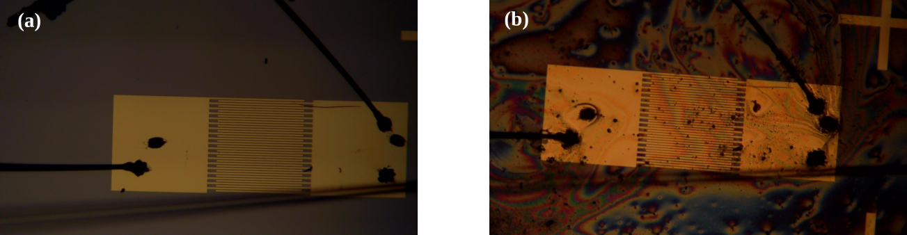
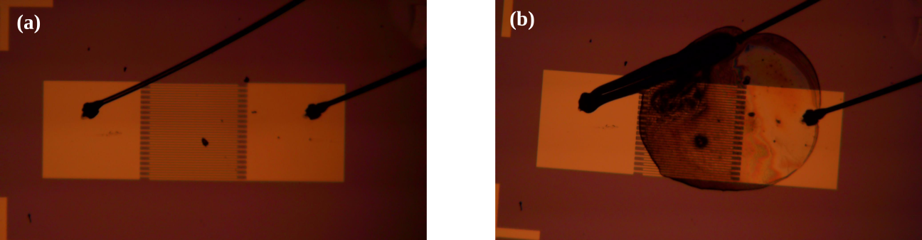
6.7 Supplement F: Photodetector Drop-Casts
A range of photodetector parameters were tested in various combinations creating 4 sets of photodetectors with the same geometries, L , S , and A . Selected photodetectors were used for characterizing the quality and variability of drop-cast NCs as seen in figures: 20, 21, 22, 23, and 24.