Enhancement in neuromorphic NbO2 memristive device switching at cryogenic temperatures
Abstract
The electrical properties and performance characteristics of niobium dioxide (NbO2)-based memristive devices are examined at cryogenic temperatures. Sub-stoichiometric Nb2O5 was deposited via magnetron sputtering and patterned in microscale (22 - 1515 m2) cross-bar Au/Ru/NbOx/Pt devices and electroformed at 3-5 V to make NbO2 filaments. At cryogenic temperatures, the threshold voltage () increased by more than a factor of 3. The hold voltage () was significantly lower than the threshold voltage for fast voltage sweeps (200 ms per measurement). If the sample is allowed to cool between voltage measurements, the hold voltage increases, but never reaches the threshold voltage, indicating the presence of non-volatile Nb2O5 in the filament. The devices have an activation energy of eV, lower than other NbO2 devices reported. Our works shows that even nominally “bad” memristive devices can be improved by reducing the leakage current and increases the sample resistance at cryogenic temperatures.
I Introduction
As the demand for computational power increases, the energy efficiency and scaling limitations of conventional CMOS-based circuits have become increasingly apparent. The rapidly developing field of neuromorphic computing seeks to overcome these limitations by emulating the functions of the human brain.Islam et al. (2023) The goal of neuromorphic computing is to revolutionize memory storage and computational paradigms by offering non-volatile storage and analog computing capabilities within the same architecture. In order to realize the goals of neuromorphic circuits, materials must be found that can mimic both the synaptic and neuronal behaviors in nerve cells.Indiveri et al. (2013); Jo et al. (2010); Yang, Strukov, and Stewart (2013); Wright, Hosseini, and Diosdado (2013); Hasler and Marr (2013); Pickett, Medeiros-Ribeiro, and Williams (2013)
Crystalline niobium dioxide has emerged as a material of significant interest in neuromorphic circuits, for example, as a scalable neuristor,Pickett, Medeiros-Ribeiro, and Williams (2013) as selectors in non-volatile RAM,Gibson et al. (2016) or as oscillator neuron devices.Kwon et al. (2023) NbO2 has a structural phase transition at approximately ∘C that is marked by a sharp insulator-metal transition (IMT), dramatically changing the resistance of the material.Sakata (1969); Janninck and Whitmore (1966); Wahila et al. (2019); Páez Fajardo et al. (2021) Reliable threshold switching about the IMT enables the precise control of the device’s resistance state, a prerequisite for the reliable operation of neuromorphic circuits.Liu et al. (2014)
The preferred oxidation state of niobium oxide is Nb2O5, which makes deposition of crystalline NbO2 challenging. While many studies successfully deposit NbO2 films (sometimes crystallinePark et al. (2016, 2017) though more often amorphous or poly-crystallineKumar et al. (2017); Joshi, Borisov, and Lederman (2018); Stoever et al. (2020)), most researchers deposit Nb2O5 Li et al. (2018); Nath et al. (2020, 2021) or a mixture of NbO, Nb2O5, and NbO2 (usually referred to as NbOx) Gibson et al. (2016); Kozen et al. (2020); Chen et al. (2021a, b); Sullivan et al. (2022), or intentionally layer NbO2 and Nb2O5Liu et al. (2014); Nandi et al. (2015a, 2020); Lee et al. (2021) or layer NbO and NbOxPark et al. (2022). In some reports, the exact composition of the NbOx films is unclear.Chen et al. (2018); Wang, Khan, and Yu (2020); Kwon et al. (2023)
If the initially deposited film is not NbO2, researchers must create NbO2 from the as-deposited film. The most straightforward method is post-deposition annealing,Kumar et al. (2017); Stoever et al. (2020); Park et al. (2022); Páez Fajardo et al. (2021); Fridriksson et al. (2022); Sullivan et al. (2022) with a wide range of annealing temperatures, pressures, and ambient gases. The more common method is to create an electroformed NbO2 filament by applying a large voltage across the film between the bottom and the top electrode.Nandi et al. (2015a); Park et al. (2016); Chen et al. (2018); Joshi, Borisov, and Lederman (2018); Li et al. (2018); Nath et al. (2020); Nandi et al. (2020); Chen et al. (2021a); Nath et al. (2021); Sullivan et al. (2022); Kwon et al. (2023) These electroformed devices are usually a crystalline NbO2 filament of nmNandi et al. (2020) surrounded by amorphous NbO2 and Nb2O5Kwon et al. (2023). Some researchers combine annealing and electroforming,Lee et al. (2021) and some are unclear how they form NbO2.Wang, Khan, and Yu (2020)
Finally, memristive NbO2 devices typically come in one of two forms. The most common is a simple cross-bar geometry, where the NbOx layer is sandwiched between two metal electrodes. In the cross-bar geometry, the typical device sizes range from 22 to 4040 m2. Liu et al. (2014); Nandi et al. (2015a, b); Park et al. (2017); Chen et al. (2018); Li et al. (2018); Nandi et al. (2020); Chen et al. (2021a); Nath et al. (2020); Wang, Khan, and Yu (2020); Nath et al. (2021); Park et al. (2022); Sullivan et al. (2022); Kwon et al. (2023); Chen et al. (2022) These devices nearly always require the stochastic electroforming step, and the electroformed NbO2 filaments are nearly always much smaller than the device size.Nandi et al. (2020) Some devices of this type rely on a percolation path through the crystalline NbO2.Lee et al. (2021) Less common is a nanoscale-sized bottom electrode (2020 to 200200 nm2) photolithographically patterned as a small metal via through an insulating layer, covered with a blanket niobium oxide film and a large top electrode.Gibson et al. (2016); Kumar et al. (2017); Kozen et al. (2020); Lee et al. (2021); Sullivan et al. (2022) These films greatly constrain the device size to be about the size of an electroformed filament or smaller.
Given the wide range of NbOx films and devices, it is not surprising that there is a wide range of switching behaviors in NbO2 memristors. Many published reports have found threshold switching behavior with on and off-state resistances (or currents) that can change by an order of magnitude (and often more).Liu et al. (2014); Nandi et al. (2015a, b); Mikolajick et al. (2016); Park et al. (2017); Chen et al. (2018); Li et al. (2018); Nandi et al. (2020); Chen et al. (2021a); Lee et al. (2021); Nath et al. (2020); Wang, Khan, and Yu (2020); Nath et al. (2021); Park et al. (2022); Sullivan et al. (2022); Kwon et al. (2023); Chen et al. (2022); Sullivan et al. (2022) On occasion, researchers have reported NbO2 films that display non-ohmic behavior but without an abrupt switch from high to low resistance state.Chen et al. (2021b); Lee et al. (2021); Sullivan et al. (2022) Controlling the behavior of NbO2 to achieve repeatable and reliable memristive devices is a key goal of researchers in this field.
We have deposited films of sub-stiochiometric Nb2O5 via physical vapor deposition and created devices in the common cross-bar geometry, with device sizes ranging from 22 - 1515 m2. We electroformed an NbO2 filament which gave poor memristive behavior at room temperature.Sullivan et al. (2022) In this work, we examined the behavior of the NbO2 filaments at cryogenic temperatures. In all cases, the threshold voltage increased and the resistive ratio between the off and on states also increased (high and low resistance states), improving the memristive device characteristics.
II Experiment
All NbO2 films were deposited at the University at Albany College of Nanotechnology, Science & Engineering in a Kurt J. Lesker PVD75 system via reactive magnetron sputtering using targets purchased from Kurt J. Lesker. The deposition occurred in an oxygen poor environment at 25∘C at 3% O2 flow in Ar atmosphere at 3 mTorr with a target power density of 6 W/cm2. This process yields sub-stoichiometric amorphous Nb2O5 after the deposition which can be crystallized into the metastable allotrope NbO2.
X-ray photoelectron spectroscopy (XPS) was measured with a Kratos Axis Ultra DLD, which has a monochromatic Al-k X-ray source, and hemispherical analyzer. Survey spectra were measured with a pass energy of 100 eV, and high resolution spectra were measured with a pass energy of 20 eV. XPS data were analyzed with the CasaXPS software package.
Atomic force microscopy images were taken with a Park System AFM in tapping mode. The measurements were performed in air. We used the open-source software package Gwyddion to analyze our data.
The cross-bar device structures were fabricated at the Cornell NanoScale Science and Technology Facility with 50 nm-thick Pt bottom electrodes ranging in width from 2 m to 15 m on SiO2. Blanket NbOx deposition occurred on top of the bottom electrode, and then capped with a top electrode of a 10 nm adhesion layer of Ru followed by 50 nm of either Au or Pt. Device patterning used standard liftoff photolithography and RIE for cleaning and to etch through the NbOx layer to reach the bottom electrode. The schematic of the cross devices is shown as an inset in Fig. 1. The NbOx films in the cross-bar devices were not thermally annealed after deposition.
The electric behavior of the devices were measured using a Keithley 2400 Source Measure Unit in voltage control mode with a compliance current of 1 mA. IV curves were initially swept from -1 to 1 V, with some sweeps reaching voltages as high as 5 V to create the electroformed NbO2 filaments. The devices were cooled to low temperatures in a Janis closed-cycle cryostat. The temperature was monitored using a Lakeshore 336 temperature controller.

III Results and Discussion
III.1 Sample growth and characterization
The as-grown materials were characterized with XPS, XRD, and AFM. Characterization was measured on blanket film depositions using similar deposition conditions as on the device substrates.
XPS survey scans indicate the presence of Nb, O, and adventitious C contamination. High resolution scans for binding energies corresponding to the niobium 3d doublet can be found in Figure 1, with large peaks at around 207.7 eV and 210.4 eV, which correspond to the doublet for Nb2O5 (+5 oxidation state). A second, vanishingly small, doublet corresponding to the +4 oxidation state of NbO2 occurs roughly eV lower than the doublet for the +5 oxidation state. Typically, when NbO2 is exposed to atmospheric conditions, it will form a thin surface oxide of Nb2O5 due to the interaction with atmospheric oxygen. Wahila et al. (2019); Páez Fajardo et al. (2021); Twigg et al. (2021); Kozen et al. (2022) However, for NbO2 bulk films, the surface oxide is typically limited to the top 1.5 nm to 2.5 nm, and XPS is expected to show strong NbO2 doublet peaks which corresponds to the underlying NbO2 film Kozen et al. (2020). The lack of a significant secondary doublet implies that the as-grown film is almost exclusively Nb2O5.
The AFM images look qualitatively similar between all samples. A representative image can be found in Figure 1, with RMS roughness for the sample at 0.33 nm. XRD measurements indicate that the as-grown films are amorphous, with crystalline NbO2 developing upon annealing at 600 to 900 ∘CSullivan et al. (2022). The films in this study were not annealed.
III.2 Cryogenic measurements of NbO2 filaments
We present our results on cryogenic measurements on a typical electroformed NbO2 filament in Fig. 2. At room temperature, this device shows a gradual change in resistance to the compliance current (1 mA) and makes a poor memristive device, as reported previously.Sullivan et al. (2022) As the temperature decreases, the device resistance, the threshold voltage, , and the resistance off/on ratio, , all increase significantly. This increase in device resistivity is understood as not only the increase in resistance of the crystalline NbO2 filament, but also the suppression of the leakage current, that is, the current that flows through the amorphous matrix surrounding the NbO2 filament.Kwon et al. (2023) As the current that flows through the amorphous material decreases, the signal becomes dominated by the crystalline NbO2 filament, allowing the the sharp change in resistance due to the structural IMT phase change to become apparent at about 200 K.

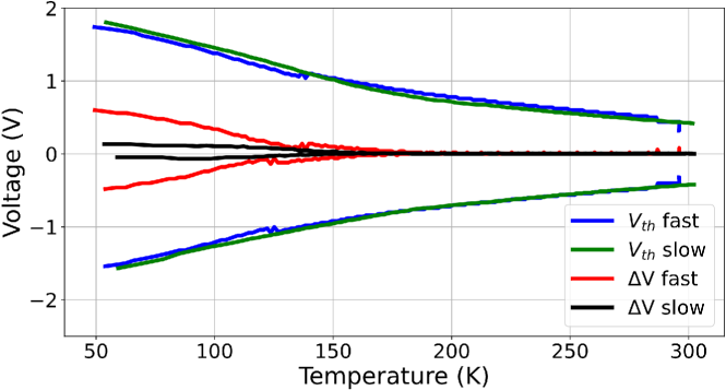
For excellent device performance, memristive devices should have a large and a large . The change in the threshold voltage as a function of temperature is presented in Fig. 3. This increase in threshold voltage has been seen in other work,Wang, Khan, and Yu (2020); Chen et al. (2021a); Kwon et al. (2023) though in the increase in in our devices is roughly a factor of 2 larger than has been reported in the literature previously, indicating that cryogenic temperatures have improved our device performance beyond that reported previously. This indicates that sub-stoichiometric Nb2O5 creates devices that have a more pronounced sensitivity to temperature changes.
In addition to high threshold voltages, a large separation between the hold and threshold voltages is required for memristive device performance. Fig. 3 also presents our results on the hold voltage. We expect the device to remain in the low-resistance “on” state for voltages lower than the threshold voltage as the device remains above the IMT temperature (about 800∘C). We find the hold voltage to be dependent on the rate of the voltage bias ramp. A 200 ms integration time per measurement gives a at or above 200 K, similar to or slightly smaller than the differences reported on previous cryogenic measurements.Wang, Khan, and Yu (2020); Chen et al. (2021a); Kwon et al. (2023) The hold voltage stays constant as temperature decreases, leading to an increase in to nearly 0.6 V at 50 K, as shown in Fig. 3.
However, longer integration times or pauses between measurements can allow the sample to cool down, which will cause the device to go through the IMT at higher hold voltages. In Fig. 3, we also present data where the voltage source was turned off for 1 s between measurements, allowing the device to cool between measurements. We show that decreases significantly, but that despite expectations, , indicating a non-volatile material embedded in series with the filament. While NbO2 can mimic the volatile neuronal behavior of nerve cells, the as-grown material, Nb2O5, is attractive because it can mimic the non-volatile synaptic functions of nerve cells.Slesazeck et al. (2015); Kumar, Strachan, and Williams (2017); Nath et al. (2021) Numerical models of the IMT in NbO2 filaments often require the incorporation of Nb2O5 regions to fully describe the behavior of the filaments.Liu et al. (2016); Chen et al. (2021a, 2022) Our results support the inclusion of such non-volatile Nb2O5 layers, as evidenced by the separation between the threshold and hold voltages, even when the device is allowed to cool down.
III.3 Threshold Power
The IMT in NbO2 is a thermally-driven transition at ∘C, and this high temperature is achieved by simple Joule heating in the sample. In cross-bar filament devices, the device area can change, but the filament cross-sectional area stays constant.Sullivan et al. (2022) This means that the power necessary to heat the material to the phase transition, , also stays constant for various device sizes.Li et al. (2018) Because the thermal conductivity of our material stack (gold and platinum) varies by less than 10% between 50 and 300 K, we expect the power needed to induce a thermal transition should also stay constant in our devices, even as the temperature decreases or the sample resistance increases. Our measurements of are presented in Fig. 4 and show that once the leakage current is suppressed and the IMT becomes obvious in the IV curves at around 200 K, the threshold power becomes constant, as expected for the thermally driven transition.

III.4 Resistance Measurements
Careful study of the resistance in these devices can give a better understanding of the underlying state of NbO2. For low electric fields, the electrical resistivity (or conductivity) is expected to vary as:Nandi et al. (2015a); Gibson et al. (2016); Stoever et al. (2020)
| (1) |
where is a constant and is the activation energy. Arrhenius plots in NbO2 memristive devices show linear behavior and activation energies between 0.15 and 0.24 eV (when measured from 300 K to 400 K),Gibson et al. (2016); Nath et al. (2021) and measurements on thin film NbO2 give an Arrhenius plot that varies smoothly from eV at cryogenic temperatures ( 200 K) to eV near the IMT temperature.Stoever et al. (2020)
To measure the material resistance at low electric fields, researchers typically choose a voltage far from the threshold voltage, usually between at or near 0.5 V,Nath et al. (2021); Lee et al. (2021) in order to ensure that the material is ohmic in nature.Gibson et al. (2016) Ohmic behavior is necessary to separate the intrinsic behavior of the NbO2 filament from the effects of Joule heating in the sample. We analyzed for our samples, and found that our sample was non-ohmic over the entire range of temperatures and voltages measured, even at the lowest measured voltages (0.03 V). Above K, the measured resistances at the two lowest voltages (0.03 V and 0.06 V) differed by less than 1%, indicating minimal effects due to Joule heating. Below 200 K, the percent change in between the lowest measured voltages increased smoothly to more than 20% at 80 K, indicating strong Joule heating in the sample even at very low bias voltages (0.03 V).
Our measurements of the device resistance are presented in an Arrhenius plot in Fig. 5. We presented at the lowest measured resistance, 0.03 V, as well as a conventional choice, 0.4 V. Above 200 K, the Arrhenius curve is linear for 0.03 V, and we find an activation energy of eV. This activation energy is lower than the eV reported for NbO2 devices,Nath et al. (2021); Gibson et al. (2016) and significantly lower than eV reported for thin-film NbO2.Stoever et al. (2020) Below 200 K in Fig. 5, we see a smoothly varying curve for 0.03 V, similar to results in thin-film NbO2,Stoever et al. (2020) and due to the significant Joule heating, a line fit is not possible.
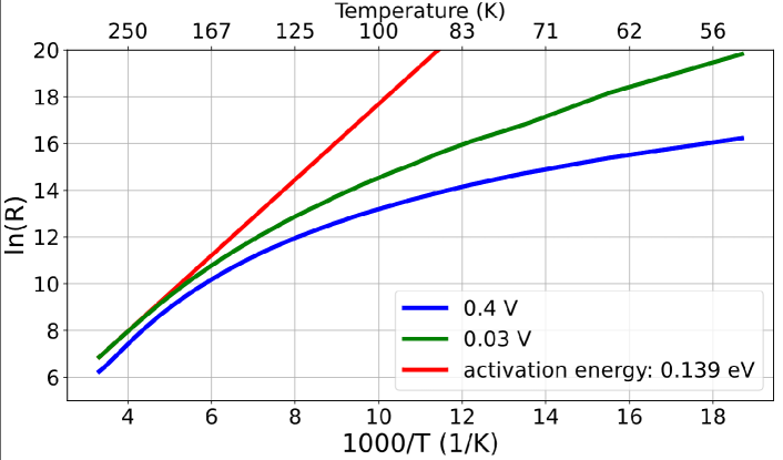
In order to compare our devices to others reported in the literature, we have also included the measured at 0.4 V in Fig. 5. At 0.4 V, the device has a lower resistance compared to the measurements at 0.03 V, which we expect, as the higher temperature at 0.4 V due to Joule heating leads to higher device temperatures. Above K, the slope at 0.4 V matches the slope at 0.03 V, meaning the activation energy is similar at K.
The results in our filament devices are correlated: The lower activation energy in the device leads directly to both the lower resistance and the poor switching behavior when compared with other filament devices at room temperature. As a result, we can conclude that as-grown sub-stoichiometric Nb2O5 is not a good candidate for NbO2 devices via electroformation. The low activation energy in this material means that the resistance in these devices must be increased before it can be useful for memristors —this can be accomplished by decreasing the temperature, or by decreasing the device size.Sullivan et al. (2022)
IV Conclusion
We have studied filamentary devices electroformed from as-deposited sub-stoichiometric Nb2O5. At room temperature, these devices are poor candidates for memristive applications, with low threshold voltages and with an ratio near zero.Sullivan et al. (2022)
Cryogenic measurements of these same devices show a marked increase in resistance due to the suppression of leakage currents. Below 200 K, the filaments display a large increase in the threshold voltage driven by the increase in the device resistance at lower temperatures. Nevertheless, the power required to heat the sample to the IMT temperature stays constant, as expected for this thermally-driven transition. The off/on resistance ratio increases to values between 10 and 50, and the hold voltage is significantly lower than the threshold voltage for rapid voltage sweeps. Thus, at cryogenic temperatures, the device performance improves significantly.
There is a wide variety of NbO2 and Nb2O5 films currently being used by researchers in efforts to optimize the niobium oxide’s performance for memristive devices. Some of the widely varying results come from the lack of clarity in growth conditions and lack of clarity in the underlying niobium oxide films used for devices. However, our results indicate that even nominally “bad” films can be used for memristive devices if steps are taken to reduce the leakage current and increase the device resistance: through percolation paths and incomplete annealing,Lee et al. (2021) through annealing and nanoscale device sizes,Sullivan et al. (2022) or through operation at cryogenic temperatures.
Acknowledgements.
This research was supported by the National Science Foundation grants nos. DMR-2103197, DMR-2103185 and the Air Force Research Laboratory grant FA8750-21-1-1019. This work was performed in part at the Cornell NanoScale Facility, a member of the National Nanotechnology Coordinated Infrastructure (NNCI), which is supported by the National Science Foundation (Grant NNCI-2025233) and made use of the Cornell Center for Materials Research Shared Facilities, which are supported through the NSF MRSEC program (DMR-1719875). The niobium oxide films were grown at the Albany Nanotech Complex via NY CREATES and Dr. Sandra Schujman at NY CREATES assisted with x-ray measurements.Data Availability The data that support the findings of this study are available from the corresponding author upon reasonable request.
Conflicts of Interest The authors have no conflicts to disclose.
References
- Islam et al. (2023) M. M. Islam, S. Alam, M. S. Hossain, K. Roy, and A. Aziz, “A review of cryogenic neuromorphic hardware,” Journal of Applied Physics 133, 070701 (2023), https://pubs.aip.org/aip/jap/article-pdf/doi/10.1063/5.0133515/16749144/070701_1_online.pdf .
- Indiveri et al. (2013) G. Indiveri, B. Linares-Barranco, R. Legenstein, G. Deligeorgis, and T. Prodromakis, “Integration of nanoscale memristor synapses in neuromorphic computing architectures,” Nanotechnology 24, 384010 (2013).
- Jo et al. (2010) S. H. Jo, T. Chang, I. Ebong, B. B. Bhadviya, P. Mazumder, and W. Lu, “Nanoscale memristor device as synapse in neuromorphic systems,” Nano Letters 10, 1297–1301 (2010), pMID: 20192230.
- Yang, Strukov, and Stewart (2013) J. J. Yang, D. B. Strukov, and D. R. Stewart, “Memristive devices for computing,” Nature Nanotechnology 8, 13–24 (2013), pMID: 20192230.
- Wright, Hosseini, and Diosdado (2013) C. D. Wright, P. Hosseini, and J. A. V. Diosdado, “Beyond von-Neumann computing with nanoscale phase-change memory devices,” Advanced Functional Materials 23, 2248–2254 (2013), https://onlinelibrary.wiley.com/doi/pdf/10.1002/adfm.201202383 .
- Hasler and Marr (2013) J. Hasler and B. Marr, “Finding a roadmap to achieve large neuromorphic hardware systems,” Frontiers in neuroscience 7, 118 (2013).
- Pickett, Medeiros-Ribeiro, and Williams (2013) M. D. Pickett, G. Medeiros-Ribeiro, and R. S. Williams, “A scalable neuristor built with Mott memristors,” Nature materials 12, 114–117 (2013).
- Gibson et al. (2016) G. A. Gibson, S. Musunuru, J. Zhang, K. Vandenberghe, J. Lee, C.-C. Hsieh, W. Jackson, Y. Jeon, D. Henze, Z. Li, and R. Stanley Williams, “An accurate locally active memristor model for s-type negative differential resistance in NbOx,” Applied Physics Letters 108, 023505 (2016), https://doi.org/10.1063/1.4939913 .
- Kwon et al. (2023) O. Kwon, S. Heo, D. Kim, J. Kim, and H. Hwang, “Enhancement of nbo2-based oscillator neuron device performance via cryogenic operation,” Nanotechnology 35, 105203 (2023).
- Sakata (1969) K. Sakata, “Note on the phase transition in NbO2,” Journal of the Physical Society of Japan 26, 582–582 (1969).
- Janninck and Whitmore (1966) R. Janninck and D. Whitmore, “Electrical conductivity and thermoelectric power of niobium dioxide,” Journal of Physics and Chemistry of Solids 27, 1183–1187 (1966).
- Wahila et al. (2019) M. J. Wahila, G. Paez, C. N. Singh, A. Regoutz, S. Sallis, M. J. Zuba, J. Rana, M. B. Tellekamp, J. E. Boschker, T. Markurt, J. E. N. Swallow, L. A. H. Jones, T. D. Veal, W. Yang, T.-L. Lee, F. Rodolakis, J. T. Sadowski, D. Prendergast, W.-C. Lee, W. A. Doolittle, and L. F. J. Piper, “Evidence of a second-order peierls-driven metal-insulator transition in crystalline ,” Phys. Rev. Materials 3, 074602 (2019).
- Páez Fajardo et al. (2021) G. J. Páez Fajardo, S. A. Howard, E. Evlyukhin, M. J. Wahila, W. R. Mondal, M. Zuba, J. E. Boschker, H. Paik, D. G. Schlom, J. T. Sadowski, S. A. Tenney, B. Reinhart, W.-C. Lee, and L. F. J. Piper, “Structural phase transitions of NbO2: Bulk versus surface,” Chemistry of Materials 33, 1416–1425 (2021).
- Liu et al. (2014) X. Liu, S. K. Nandi, D. K. Venkatachalam, K. Belay, S. Song, and R. G. Elliman, “Reduced threshold current in nbo2 selector by engineering device structure,” IEEE Electron Device Letters 35, 1055–1057 (2014).
- Park et al. (2016) J. Park, E. Cha, I. Karpov, and H. Hwang, “Dynamics of electroforming and electrically driven insulator-metal transition in nbox selector,” Applied Physics Letters 108, 232101 (2016), https://doi.org/10.1063/1.4953323 .
- Park et al. (2017) J. Park, T. Hadamek, A. B. Posadas, E. Cha, A. A. Demkov, and H. Hwang, “Multi-layered NiOy/NbOx/NiOy fast drift-free threshold switch with high Ion/Ioff ratio for selector application,” Scientific Reports 7, 4068 (2017).
- Kumar et al. (2017) S. Kumar, Z. Wang, N. Davila, N. Kumari, K. J. Norris, X. Huang, J. P. Strachan, D. Vine, A. D. Kilcoyne, Y. Nishi, and R. S. Williams, “Physical origins of current and temperature controlled negative differential resistances in nbo2,” Nature Communications 8, 658 (2017).
- Joshi, Borisov, and Lederman (2018) T. Joshi, P. Borisov, and D. Lederman, “Structural and electrical characterization of polycrystalline nbo2 thin film vertical devices grown on tin-coated sio2/si substrates,” Journal of Applied Physics 124, 114502 (2018), https://doi.org/10.1063/1.5038837 .
- Stoever et al. (2020) J. Stoever, J. E. Boschker, S. Bin Anooz, M. Schmidbauer, P. Petrik, J. Schwarzkopf, M. Albrecht, and K. Irmscher, “Approaching the high intrinsic electrical resistivity of NbO2 in epitaxially grown films,” Applied Physics Letters 116, 182103 (2020), https://pubs.aip.org/aip/apl/article-pdf/doi/10.1063/5.0005523/8743467/182103_1_online.pdf .
- Li et al. (2018) S. Li, X. Liu, S. K. Nandi, and R. G. Elliman, “Anatomy of filamentary threshold switching in amorphous niobium oxide,” Nanotechnology 29, 375705 (2018).
- Nath et al. (2020) S. K. Nath, S. K. Nandi, S. Li, and R. G. Elliman, “Metal-oxide interface reactions and their effect on integrated resistive/threshold switching in NbOx,” Nanotechnology 31, 235701 (2020).
- Nath et al. (2021) S. K. Nath, S. K. Nandi, T. Ratcliff, and R. G. Elliman, “Engineering the threshold switching response of Nb2O5-based memristors by ti doping,” ACS Applied Materials & Interfaces 13, 2845–2852 (2021), pMID: 33406833, https://doi.org/10.1021/acsami.0c19544 .
- Kozen et al. (2020) A. C. Kozen, Z. R. Robinson, E. R. Glaser, M. Twigg, T. J. Larrabee, H. Cho, S. M. Prokes, and L. B. Ruppalt, “In situ hydrogen plasma exposure for varying the stoichiometry of atomic layer deposited niobium oxide films for use in neuromorphic computing applications,” ACS Applied Materials & Interfaces 12, 16639–16647 (2020), pMID: 32223206, https://doi.org/10.1021/acsami.0c01279 .
- Chen et al. (2021a) A. Chen, Z. Zhang, G. Ma, N. Liu, C.-Y. Lin, W.-C. Chen, T.-C. Chang, and H. Wang, “Comprehensive regulation of the threshold oscillation for neuromorphic systems based on cryogenic performance of nbo2 device,” IEEE Electron Device Letters 42, 692–695 (2021a).
- Chen et al. (2021b) D. Chen, A. Chen, Z. Yu, Z. Zhang, Q. Tan, J. Zeng, J. Ji, X. Pan, G. Ma, H. Wan, Y. Rao, L. Tao, X. Peng, J. Duan, H. Wang, and T.-C. Chang, “Forming-free, ultra-high on-state current, and self-compliance selector based on titanium-doped NbOx thin films,” Ceramics International 47, 22677–22682 (2021b).
- Sullivan et al. (2022) M. C. Sullivan, Z. R. Robinson, K. Beckmann, A. Powell, T. Mburu, K. Pittman, and N. Cady, “Threshold switching stabilization of NbO2 films via nanoscale devices,” Journal of Vacuum Science & Technology B 40, 063202 (2022), https://pubs.aip.org/avs/jvb/article-pdf/doi/10.1116/6.0002129/16571686/063202_1_online.pdf .
- Nandi et al. (2015a) S. K. Nandi, X. Liu, D. K. Venkatachalam, and R. G. Elliman, “Threshold current reduction for the metal–insulator transition in NbO2-x-selector devices: the effect of ReRAM integration,” Journal of Physics D: Applied Physics 48, 195105 (2015a).
- Nandi et al. (2020) S. K. Nandi, S. K. Nath, A. E. El-Helou, S. Li, T. Ratcliff, M. Uenuma, P. E. Raad, and R. G. Elliman, “Electric field- and current-induced electroforming modes in NbOx,” ACS Applied Materials & Interfaces 12, 8422–8428 (2020), pMID: 31989818, https://doi.org/10.1021/acsami.9b20252 .
- Lee et al. (2021) J. Lee, J. Kim, J. Jeong, and H. Sohn, “Electroforming and threshold switching characteristics of NbOx films with crystalline NbO2 phase,” Journal of Vacuum Science & Technology B 39, 053206 (2021), https://doi.org/10.1116/6.0001215 .
- Park et al. (2022) K. Park, J. Ryu, D. P. Sahu, H.-M. Kim, and T.-S. Yoon, “Electroforming-free threshold switching of NbOx–based selector devices by controlling conducting phases in the NbOx layer for the application to crossbar array architectures,” RSC Adv. 12, 18547–18558 (2022).
- Chen et al. (2018) A. Chen, G. Ma, Y. He, Q. Chen, C. Liu, H. Wang, and T.-C. Chang, “Research on temperature effect in insulator–metal transition selector based on NbOx thin films,” IEEE Transactions on Electron Devices 65, 5448–5452 (2018).
- Wang, Khan, and Yu (2020) P. Wang, A. I. Khan, and S. Yu, “Cryogenic behavior of NbO2 based threshold switching devices as oscillation neurons,” Applied Physics Letters 116, 162108 (2020), https://pubs.aip.org/aip/apl/article-pdf/doi/10.1063/5.0006467/13883086/162108_1_online.pdf .
- Fridriksson et al. (2022) E. Fridriksson, T. Tryggvason, U. Arnalds, A. Ingason, and F. Magnus, “Growth of NbO, NbO2 and Nb2O5 thin films by reactive magnetron sputtering and post-annealing,” Vacuum 202, 111179 (2022).
- Nandi et al. (2015b) S. K. Nandi, X. Liu, D. K. Venkatachalam, and R. G. Elliman, “Self-assembly of an NbO2 interlayer and configurable resistive switching in Pt/Nb/HfO2/Pt structures,” Applied Physics Letters 107, 132901 (2015b), https://doi.org/10.1063/1.4932096 .
- Chen et al. (2022) P. Chen, X. Zhang, Q. Liu, and M. Liu, “NbO2-based locally active memristors: from physical mechanisms to performance optimization,” Applied Physics A: Materials Science & Processing 128, 1113 (2022).
- Mikolajick et al. (2016) T. Mikolajick, H. Wylezich, H. Maehne, S. Slesazeck, and T. Mikolajick, “Versatile resistive switching in niobium oxide,” in 2016 IEEE International Symposium on Circuits and Systems (ISCAS) (2016) pp. 381–384.
- Twigg et al. (2021) M. Twigg, A. Kozen, L. Ruppalt, S. Prokes, and H. Cho, “Transmission electron microscopy analysis of reduction reactions and phase transformations in Nb2O5 films deposited by atomic layer deposition,” Journal of Applied Physics 129, 025304 (2021).
- Kozen et al. (2022) A. Kozen, J. Woodward, L. Ruppalt, H. Cho, C. Ventrice, A. Rowley, N. Zhe, A. Mesiti, E. Sargent, J. Michels, and Z. Robinson, “Crystallization behavior of zinc doped Nb2O5 thin films synthesized by atomic layer deposition,” ACS Applied Electronic Materials In Press (2022).
- Slesazeck et al. (2015) S. Slesazeck, H. Mähne, H. Wylezich, A. Wachowiak, J. Radhakrishnan, A. Ascoli, R. Tetzlaff, and T. Mikolajick, “Physical model of threshold switching in nbo2 based memristors,” RSC Adv. 5, 102318–102322 (2015).
- Kumar, Strachan, and Williams (2017) S. Kumar, J. P. Strachan, and R. S. Williams, “Chaotic dynamics in nanoscale nbo2 mott memristors for analogue computing,” Nature 548, 318–321 (2017).
- Liu et al. (2016) X. Liu, S. Li, S. K. Nandi, D. K. Venkatachalam, and R. G. Elliman, “Threshold switching and electrical self-oscillation in niobium oxide films,” Journal of Applied Physics 120, 124102 (2016), https://pubs.aip.org/aip/jap/article-pdf/doi/10.1063/1.4963288/15185659/124102_1_online.pdf .