Single photon emitters in monolayer semiconductors coupled to transition metal dichalcogenide nanoantennas on silica and gold substrates
Panaiot G. Zoteva∗, Sam A. Randersona, Xuerong Hua, Yue Wangb, Alexander I. Tartakovskiia∗∗
aDepartment of Physics and Astronomy, University of Sheffield, Sheffield, S3 7RH, UK
bSchool of Physics, Engineering and Technology, University of York, York, YO10 5DD, UK
∗p.zotev@sheffield.ac.uk ∗∗a.tartakovskii@sheffield.ac.uk
Transition metal dichalcogenide (TMD) single photon emitters (SPEs) offer numerous advantages to quantum information applications, such as high single photon purity and deterministic positioning. Strain in the host monolayer, induced by underlying dielectric Mie resonators, is known to localize their formation to positions co-located with near-field photonic hotspots providing further control over their optical properties. However, traditional materials used for the fabrication of nanoresonators, such as silicon or gallium phosphide (GaP), often require a high refractive index substrate resulting in losses of the emitted light and limited photonic enhancement. Here, we use nanoantennas (NAs) fabricated from multilayer TMDs, which allow complete flexibility with the choice of substrate due to the adhesive van der Waals forces, enabling high refractive index contrast or the use of highly reflective metallic surfaces. We demonstrate the localized formation of SPEs in WSe2 monolayers transferred onto WS2 NAs on both SiO2 and Au substrates, enabling strong photonic enhancements and increased single photon collection. We provide evidence for enhanced quantum efficiencies (QE) reaching an average value of 43% (7%) for SPEs on WS2 NAs on a SiO2 (Au) substrate. We further combine the advantages offered by both dielectric and metallic substrates to numerically simulate an optimized NA geometry for maximum WSe2 single photon excitation, emission, collection. Thus, the fluorescence is enhanced by a factor of over 4 orders of magnitude compared to vacuum and 5 orders of magnitude compared to a flat SiO2/Si surface. Our work showcases the advantages offered by employing TMD material nanoresonators on various substrates for SPE formation and photonic enhancement.
TMD material single photon emitters have drawn much interest due to their expected use in atomically thin quantum devices which can be deterministically fabricated and integrated with arbitrary substrates, offering narrow linewidths and high single photon purity [1]. The formation mechanism of these quantum emitters, discovered first in monolayer WSe2 [2, 3, 4, 5, 6] and often associated with strain [7, 8, 9, 10, 11], is still debated. However, this has lead to the proposal of several theoretical models describing their occurrence in cryogenic photoluminescence (PL) including strain-induced potential traps for excitons [12], various defects [13, 14], both of which are believed to be filled by trapped dark excitons [8, 12, 13, 15] or via long-lived intermediate states [16], as well as momentum-dark states[17]. Despite the lack of definitive knowledge concerning their origin, many steps have been taken to integrate TMD SPEs with devices by employing focused ion beam defect formation [18] or, more commonly, strain-engineering [19, 20, 9, 10, 11] and thereby coupling to waveguides [21, 22], microcavities [23, 24], circular Bragg gratings [25] and Mie resonators [26, 27, 15]. Additionally, tuning of the properties of the SPEs has been achieved by shaping the strain profile to orient the dipole of the emitter [19, 28, 29], increasing strain values [30, 15] or using gating [31] to tune the emission energy and employing van der Waals ferromagnets to achieve chiral single photon emission [32].
Applications in quantum information requiring the scalable and controllable realization of on-chip quantum emitters have led to arrays of 2D SPEs realized by transfer of monolayer WSe2 onto pre-fabricated arrays of nanopillars patterned in photoresist [8], SiO2 [33], GaP [15] and Au/Si with a spacer layer of Al2O3 on top [27]. The latter two of these materials were employed to enhance SPE intensities by coupling with Mie resonances as a result of the close proximity of maximum strain values and photonic mode hotspots [27, 15]. However, each of these devices required the fabrication of nanopillars or Mie resonators from the substrate material thus achieving little to no refractive index contrast, known to enable strong localization of resonances and thus provide large fluorescence enhancements [34], between nanoresonator and underlying surface.
Recently, works employing van der Waals (vdW) materials as high-index dielectrics for the fabrication of nanophotonic structures [35, 36, 37, 38, 39, 40] have enabled the realization of nanoresonators on arbitrary substrates achieving a large refractive index contrast and thus tightly confined resonances [34, 41] as well as hybrid dielectric-plasmonic resonances with ultra-high Q factors [41, 42]. These vdW material nanophotonic structures thus enable many applications such as waveguiding [38, 43], strong light-matter coupling [35, 40, 41], lasing [44] and Purcell enhancement of emission [39, 45, 46].
Here, we pattern WS2 multilayer crystals deposited on SiO2 and Au substrates into hexagonal dimer nanoantennas. Through dark field spectroscopy we confirmed the presence of Mie resonances which we employed in the fluorescence enhancement of single photon emitters forming in monolayer WSe2 transferred onto the fabricated nanoresonators. Simulations of the resulting NAs on both substrates yielded strong electric field confinement into photonic hotspots at the top surface of the NAs where the strain in the transferred monolayer is expected to be highest, thus inducing the formation of SPEs. These hotspots are expected to enhance the absorption in the monolayer, increase the QE of single photon emission and improve collection efficiencies by redirecting the emitted light into our optical setup [15]. The total maximum fluorescence enhancement factor for a quantum emitter forming within these hotspots compared with one in vacuum, calculated from these three contributions, was simulated to reach as high as 914 (10670) for the SiO2 (Au) substrate. When we compare an SPE within the hotspots of the NA on a SiO2 (Au) substrate to an emitter on a flat 300 nm SiO2/Si wafer surface we calculated a fluorescence enhancement as high as 2012 (23493).
In cryogenic PL measurements, we observed the formation of spatially localized, narrow-linewidth emitters which are shown to emit single photons. We recorded a factor of 2.7 higher SPE intensity for the SiO2 substrate. Using pulsed laser excitation and simulations of the collection efficiency near each NA, we extract a quantum efficiency of each emitter. We define this as the average number of photons emitted per excitation pulse. The SPEs forming on WS2 NAs on a SiO2 (Au) substrate yielded an average QE of 43% (7%), which is higher than observed for quantum emitters in an unenhanced or weakly enhanced regime ( 1.5-4% [26, 15]). We attribute the very high average QE for the SiO2 substrate to the strong mode confinement achievable with a large refractive index contrast ( 2.5). The much lower QE of the emitters forming on NAs fabricated on the Au substrate is attributed to non-radiative decay channels from the SPE state, such as charge transfer to the metallic surface [47]. We confirm this via a reduced average SPE lifetime and the reduction of Auger processes observed in the time resolved PL of monolayer WSe2 on a flat Au substrate.
To surmount the disadvantage of increased non-radiative decay and make use of the larger collection efficiency of a metallic substrate, we further design optimized WS2 NAs on a gold substrate with an insulating spacer of SiO2 or hBN. The insulating layer is used to suppress charge transfer processes while also yielding maximum fluorescence enhancement factors of more than 23700 (33200), compared to vacuum, and more than 157900 (221300), compared to a flat 300 nm SiO2/Si surface, for a WSe2 SPE forming within the hotspots at the outer top vertices of the NAs fabricated on a Au substrate with a SiO2 (hBN) spacer under low power excitation. Our work showcases the advantages offered by heterointegration of TMD SPEs and nanoresonators with different substrates, thereby enabling optimized coupling of enhanced quantum emitters with virtually any material system and device.
Results
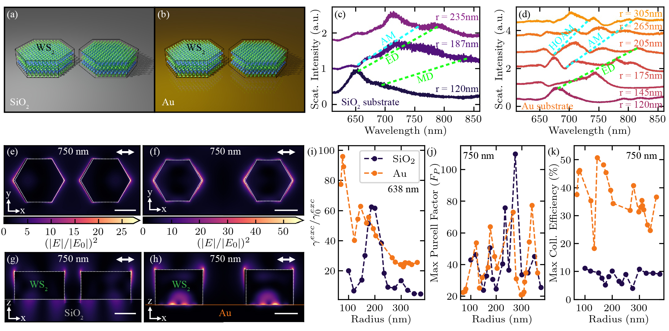
WS2 nanoantennas on SiO2 and Au substrates To achieve an entirely TMD SPE system on different substrates, we began by preparing two nominally 290 nm SiO2/Si substrates, one of which was coated with a 100 nm thick Au film sputtered by electron beam. We mechanically exfoliated multilayer WS2 crystals onto these two substrates and employed electron beam lithography and reactive ion etching to pattern hexagonal dimer (double pillar) NAs into the WS2 [39, 48]. While the SiO2 substrate was slightly overetched (<15 nm), the Au film acted as a natural etch stop [41, 42] leaving 135 nm and 190 nm tall WS2 dimer NAs on the SiO2 and Au substrates respectively (Figure 1(a) and (b)). Once fabricated, we characterized the optical resonances of the NAs on both substrates via dark field spectroscopy which yielded the presence of both magnetic and electric dipole Mie modes as well as anapole and higher order anapole resonances (Figures 1(c) and (d) for the SiO2 and Au substrate respectively). The height, radius and dimer separation gap for each NA was measured using atomic force microscopy (AFM) and scanning electron microscopy.
Using the measured geometry of the fabricated WS2 NAs, we simulated the electric field intensity enhancement values surrounding the nanostructures (Figure 1(e) and (f) for the SiO2 and Au substrates respectively). The radii of the simulated NAs were 235 nm and 205 nm, their heights were 135 nm and 190 nm and their dimer gaps (distance between individual nanopillars) were 150 nm and 515 nm for the SiO2 and Au substrates respectively. As we aimed to enhance the fluorescence rate of monolayer WSe2 SPEs, emitting near 750 nm, we simulated the expected photonic enhancement at this wavelength and observed confinement of the electric field at the top surface of the NAs. The photonic hotspots at the upper NA vertices are expected to yield higher fluorescence enhancements for the Au substrate. We attribute this to the redistribution of the electric field in the presence of a reflective surface and a reduced leakage into the substrate. As the photonic hotspots at the top surface of the NA are co-located with the highest expected strain values in a monolayer of WSe2 transferred onto these nanostructures [49], we expected a high probability of SPE formation within these hotspots and thus strong enhancement of their fluorescence. In order to calculate a fluorescence enhancement rate compared to vacuum (), we utilized the following definition [50]:
| (1) |
where the first factor ( corresponds to the excitation rate enhancement, which is governed by the electric field intensity at the position of the SPE, at the pump laser wavelength. The second factor () represents the quantum efficiency enhancement at the emission wavelength, which can be approximated by the Purcell factor for emitters with a low intrinsic QE as was demonstrated for WSe2 SPEs in an unenhanced or weakly enhanced regime ( 1.5-4% [26, 15]). The last factor () corresponds to the light collection efficiency enhancement provided by the photonic structure at the emission wavelength calculated for a numerical aperture of 0.64. In our simulations, each of the enhancement factors is calculated as a comparison to an emitter in a vacuum environment.
To understand the maximum possible fluorescence enhancement for the fabricated NAs on the SiO2 and Au substrates, we simulated the electric field intensity enhancement, Purcell factor and collection efficiency at the appropriate wavelength (638 nm for our laser excitation and 750 nm for the SPE emission wavelength) for a range of radii measured from our fabricated NAs (Figures 1(i)-(k)). From the electric field intensity simulations, we observed that for most radii achieved in our fabrication, we can expect stronger excitation rate enhancements for the Au substrate, attributed to the stronger confinement provided by the metallic film, and thus use lower power laser pumping. The Purcell factor simulations yielded similar emission enhancement rates for the two substrates which suggests similar expected QE enhancements in the SPEs on the two substrates. Perhaps the largest advantage of using an Au substrate as opposed to SiO2 is the factor of 4 enhancement of the expected collection efficiency which is also higher than previously achieved on GaP NAs [50, 15]. This is expected from a metallic mirror substrate as much of the light emitted from the SPE toward the substrate can now be reflected towards the collection optics. The maximum fluorescence enhancement factor () expected for properly positioned SPEs within the photonic hotspots when compared to vacuum, calculated by substituting in the results from Figures 1(i)-(k) into equation 1, varies from 62.5 to 914 for the SiO2 substrate and from 647.9 to 10670 for the Au substrate over the range of radii. Upon comparison with an emitter forming on a flat 300 nm SiO2/Si surface, the fluorescence enhancements vary from 137 to 2012 for the WS2 NAs on the SiO2 substrate and from 1426 to 23493 for the Au substrate over the same range of radii.
Single photon emitter formation and quantum efficiency enhancement To confirm that single photon emitters can be formed by depositing a monolayer TMD onto multilayer TMD nanoresonators fabricated on different substrates, we transfer a single layer of WSe2 onto the fabricated arrays of WS2 NAs on SiO2 and Au substrates (see Supplementary Note 1) via an all-dry polymer stamp technique (see Methods). WS2 NAs on SiO2 have already been shown to enhance the photoluminescence of monolayer WSe2 at room temperature via the Purcell effect [39], thus providing a promising starting point for enhancement of SPEs.
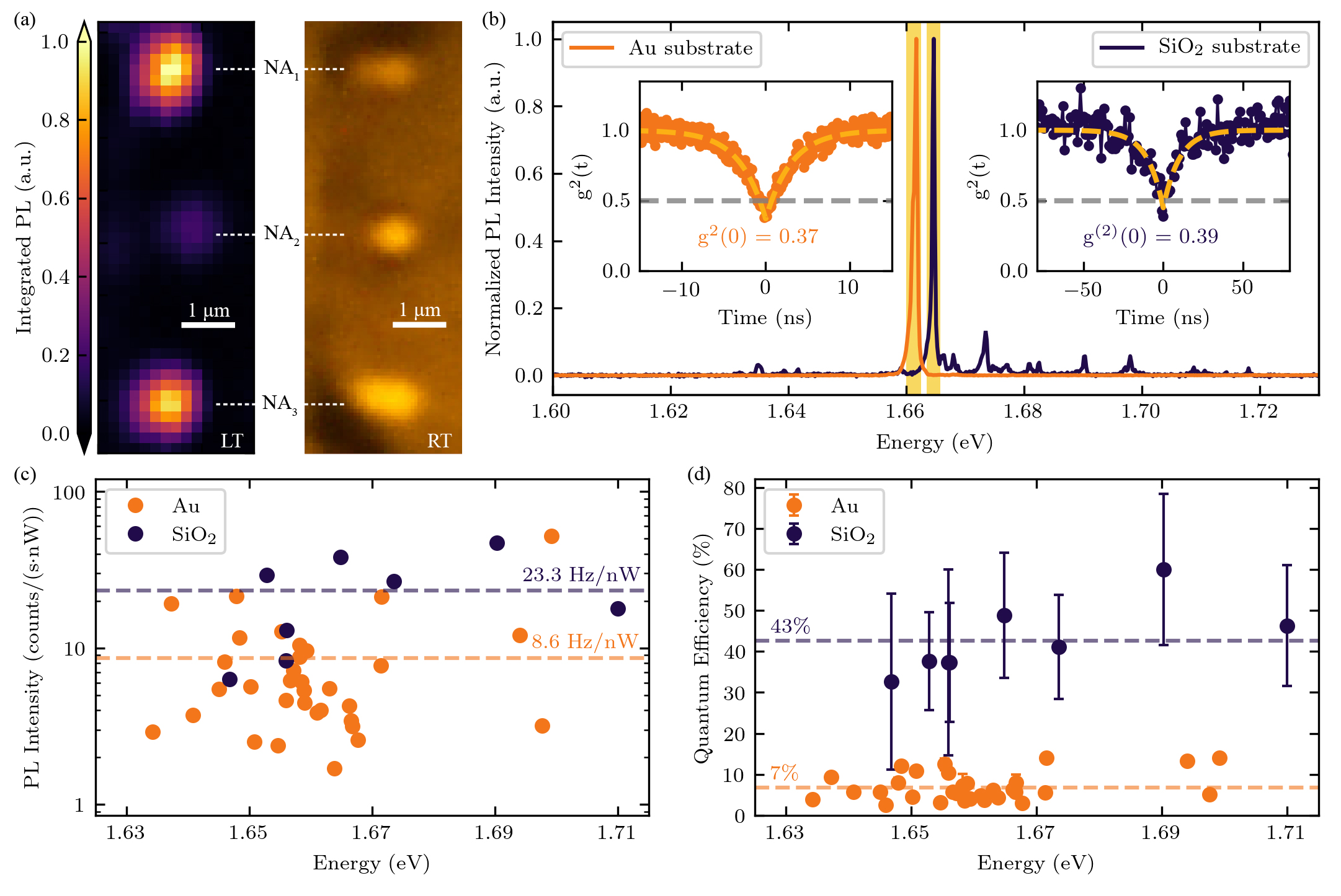
Next, we cooled our samples to liquid helium temperature in a bath cryostat and carried out detailed micro-PL experiments. We excited the WSe2 monolayer with a 638 nm pulsed laser (5MHz) and measured PL spectra from different locations at and surrounding the nanoantenna positions. We recorded a spatial map of the emitted PL, integrating between 1.663 and 1.666 eV, from the SiO2 substrate sample near three NAs (Figure 2(a), left) and compared it to a room temperature PL image, integrated between 1.24 and 2.25 eV, of the same region (Figure 2(a), right). The overlap of the low and room temperature PL in the two panels confirms that the emission is strongly localized to the NA positions. The cryogenic PL spectrum (Figure 2(b), blue) recorded from the uppermost NA in the spatial map exhibits an emitter with a linewidth of <500 eV, similar to previous reports for QE enhanced SPEs on GaP NAs [15]. A similarly narrow emission line was also observed from the WSe2 monolayer transferred onto WS2 NAs on the Au substrate (Figure 2(b), orange). We performed Hanbury-Brown-Twiss experiments (Figure 2(b), insets) to measure the photon statistics of the recorded lines from the samples with both substrates, resulting in anti-bunching dips below g2(0) = 0.5 at zero time delay, thus confirming the single photon nature of the emission. As expected for 0-D quantum emitters, we also observed linear polarization, power saturation at relatively weak excitation powers (<500 nW) and long lifetimes (7-170 ns) compared to free excitons in the WSe2 monolayer (<4 ps) [51, 52] (see Supplementary Note 2).
We recorded similar narrow-linewidth (see Supplementary Note 2) emission from nearly all of the studied NA positions (>98%) on both substrates. This provides evidence that the strain induced in the WSe2 monolayer by the WS2 NAs with heights of 135 nm and 190 nm for the SiO2 and Au substrates respectively is sufficient to induce the formation of at least one SPE at each NA position. Interestingly, many of the emitters observed on the Au substrate sample and several of those on the SiO2 surface sample exhibited a polarization along the line connecting the centers of the nanopillars forming the WS2 dimer NA (dimer axis). We attribute this to the strain profile induced in the monolayer during the transfer (see Supplementary Note 2) [19, 49]. The higher percentage of emitters forming with a polarization along the dimer axis on Au substrate sample is attributed to the larger strain induced in the monolayer by the taller NAs. This demonstrates an ability to control the polarization of the SPEs and orient it along the NA resonance expected to result in the highest photonic enhancement [39] with a more effortless procedure than in previous reports [28].
We subsequently recorded the integrated (over the linewidth of the emitter) intensities of many SPEs at saturation forming onto different WS2 NAs on the SiO2 and Au substrates (Figure 2(c)). Surprisingly, the average intensity of the emitters on the Au substrate ( 8.6 Hz/nW) is 2.7 times lower than that on the SiO2 substrate (23.3 Hz/nW) despite the overall higher excitation rate and collection efficiency enhancements we expected from the simulations in Figures 1(i) and (k). We attribute this to the introduction of a very fast non-radiative decay channel, such as charge transfer to the metallic substrate [47]. Room temperature PL and time-resolved PL measurements exhibiting reduced intensities and suppressed exciton-exciton annihilation respectively suggest such a process (see Supplementary Note 3). The reduced average lifetime of emitters recorded for the Au substrate sample as compared to those on the SiO2 surface sample (see Supplementary Note 2) provides further evidence of an increased non-radiative decay rate. We also considered that heating due to the Au substrate absorption may reduce the SPE intensities, however, the local temperature is expected to rise only negligibly (see Supplementary Note 4).
When comparing the intensities of emitters forming on WS2 NAs fabricated on the SiO2 substrate with previously studied WSe2 SPEs forming on SiO2 nanopillars [33, 8, 15] we observed larger intensities and decay lifetimes leading us to consider enhanced quantum efficiencies. As we utilized pulsed excitation with a lower laser repetition rate than the decay rates of all SPEs, expected to yield an emission rate equal to the repetition rate for a quantum efficiency of 100%, we can estimate the QE of each emitter via the following:
| (2) |
where is the recorded integrated intensity of the SPE in Hz within the saturation regime, is the simulated collection efficiency of the objective lens largely depending on the positioning of the emitter relative to the WS2 dimer NA, is the measured efficiency of our experimental setup and is the repetition rate of the excitation laser in Hz. We have measured the efficiency of our experimental setup to be 0.56% using a 725 nm laser (see Supplementary Note 5). For each emitter, we define a maximum and minimum collection efficiency based on its position relative to the NA which is unknown to us. The largest collection efficiency is found for an SPE position at the upper vertices of the NA and the lowest value is calculated for an emitter in close proximity to the substrate. Utilizing these two values provides us with not only an average estimate of the quantum efficiency of each SPE but also an upper and lower bound (Figure 2(d)) depending on the precise position of the emitter relative to the WS2 NA and substrate.
Comparing our current estimate of the QE with previously measured WSe2 SPEs forming on SiO2 nanopillars (4% [15]) and uncoupled gold nanocubes (1.5% [26]), we observed an order of magnitude higher quantum efficiencies for emitters forming on WS2 NAs on the SiO2 substrate with an average value of 43%, which is even higher than observed for quantum efficiency enhanced SPEs forming on coupled gold nanocubes (12.6% [26]) and GaP dimer nanoantennas (average 21% [15]). It is worth noting that some quantum efficiencies observed for SPEs forming on GaP nanoantennas reached higher values (86%), yet the lack of refractive index contrast between nanoantenna and substrate is expected to lead to weaker mode confinement and thus lower average QE enhancement than for the WS2 NAs on the SiO2 substrate. While the emitters forming on WS2 NAs on the Au substrate yielded a much lower average QE of 7%, this is still higher than that observed on SiO2 nanopillars or uncoupled gold nanocubes, despite the introduction of fast non-radiative charge transfer processes. We attribute this enhanced QE to two factors as discussed in a previous report [15]. First, the possibility of low power excitation leads to suppression of non-radiative exciton-exciton annihilation processes [15, 53], thereby increasing the QE of the SPEs. This factor is a result of the enhanced absorption at the pump laser wavelength as well as the reduced non-radiative processes (suggested by the long decay times compared to previous reports [3, 4]) due to either the high crystal quality of the WS2 NAs or SPE formation along suspended portions of the monolayer between contact with the dimer and the substrate. Second, Purcell enhancement of the radiative rate is expected for emitters within the NA hotspots [39] also contributing to an increased quantum efficiency.
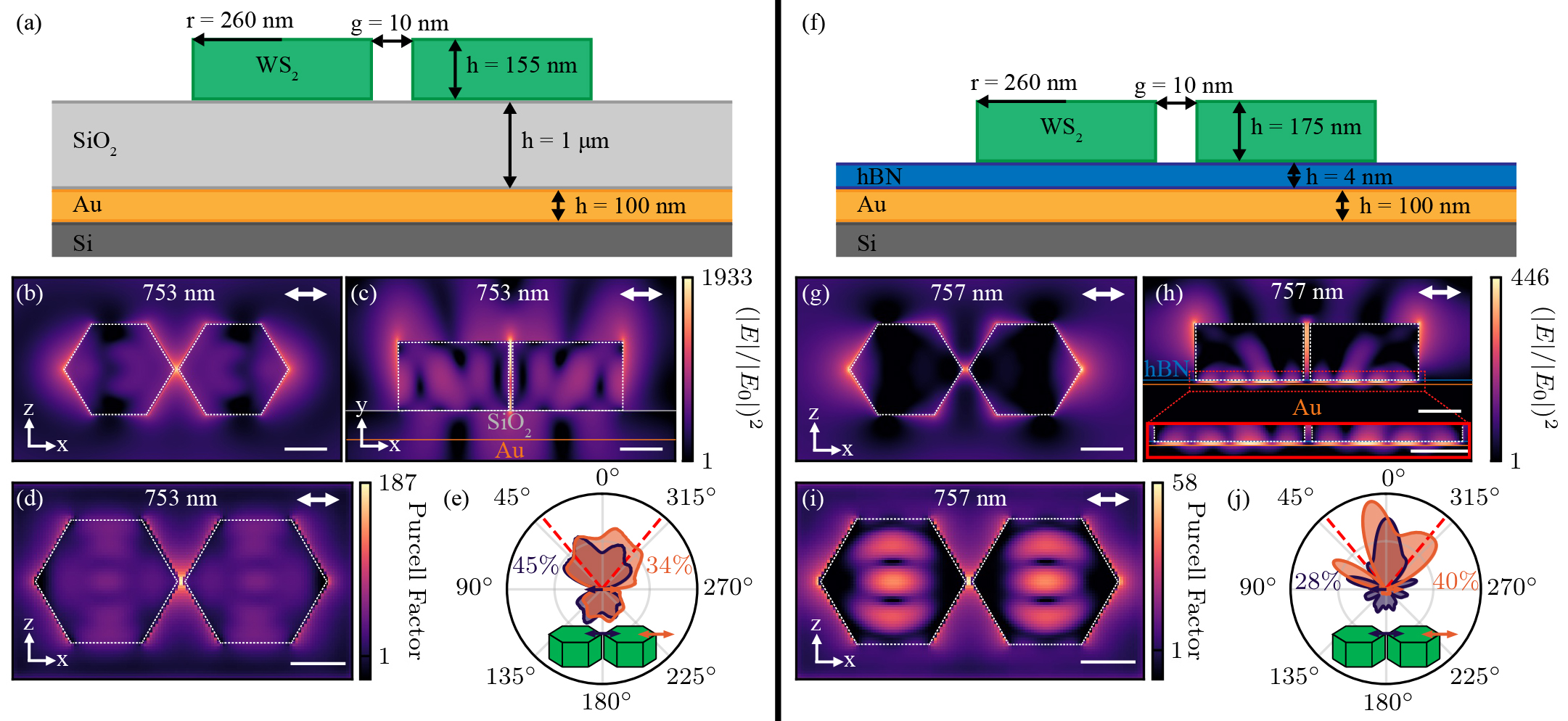
Optimized WS2 NAs on a Au substrate with a dielectric spacer As we have demonstrated so far, WS2 NAs not only enable the photonic enhancement of WSe2 single photon emitters but also offer integration with various substrates providing different advantages such as quantum efficiency or collection efficiency enhancement. To combine the advantages of the two substrates we have studied and suppress charge-transfer processes which limited SPE intensities for the Au substrate sample, we design an optimized photonic structure for maximum enhancement of WSe2 monolayer SPEs forming on WS2 dimer NAs. We consider a gold substrate with a spacer of either sputtered SiO2 (Figure 3(a)) or few-layer hBN (Figure 3(f)) below the WS2 NAs. We used FDTD simulations to calculate optimized geometries for the two different types of spacers (see Methods) leading to a radius of 260 nm, a height of 155 nm (175 nm), an ultra-small gap of 10 nm achievable through AFM repositioning [39] and a spacer layer thickness of 1 m (4 nm) for the SiO2 (hBN) spacer. These simulations were carried out with the expectation of an SPE polarization along the WS2 NA dimer axis as we observed this orientation to be more probable due to the strain profile in the transferred monolayer [19, 49] and lead to higher mode confinement [39]. The photonic resonance wavelengths were also constrained to a range coinciding with the range of discovered SPE energies in WSe2. The optimized hBN spacer is similar in thickness to an Al2O3 buffer layer (6 nm) grown atop plasmonic nanopillars, used for SPE formation and enhancement, to reduce quenching of WSe2 monolayer emission [27].
We first simulated the photonic hotspots near the upper surface of the NAs (Figure 3(b)-(c) and (g)-(h) for the SiO2 and hBN spacer design respectively) leading to excitation rate enhancements within the dimer gap of 1933 (177) for the SiO2 (hBN) spacer design. The strong confinement in the few-layer hBN spacer (Figure 3(f)) leads to far lower electric field intensity values at the top surface of the NA when compared to the SiO2 spacer design. However, the maximum electric field intensities at the outer nanoantenna vertices, where the strain in a transferred WSe2 monolayer is expected to be the highest [49] and thus most likely to form SPEs, reach far more similar values of 545 and 446 for the SiO2 and hBN spacer design respectively. The simulated electric field intensity enhancements are directly responsible for an increase in the excitation and thus the fluorescence rate if resonant excitation is employed. Precise tuning of the NA resonance wavelength can be achieved by varying the size, leading to only small reductions in the photonic enhancement in our simulations.
Next, we simulated the expected Purcell factors, directly leading to an increase in quantum efficiency and thus fluorescence rate, for WSe2 SPEs forming on the top surface of the WS2 NAs in both designs (Figure 3(d) and (i) for the SiO2 and hBN spacer design respectively). These are maximized at the inner NA vertices reaching values of 187 (58) for the SiO2 (hBN) spacer design. While the outer vertices of the NAs, where SPEs are expected to form, yielded similar Purcell factors of 22 and 32 for the SiO2 and hBN spacer designs respectively. Due to the reduced charge-transfer expected for these nanoantenna designs, we also predict far lower non-radiative rates leading to higher SPE QE and intensity than observed for the WSe2 SPEs recorded for the Au substrate sample.
Lastly we simulated the radiation pattern expected from these optimized designs, which enables the calculation of collection efficiency and thus the fluorescence rate for SPEs forming both in the dimer gap and at the more probable outer vertices of the NAs (Figures 3(e) and (j) for the for the SiO2 and hBN spacer design respectively). We observed that most of the emitted light is expected to be redirected away from the Au reflective substrate leading to a collection efficiency of 45% (28%) within our experimental numerical aperture (0.64) for an SPE forming within the dimer gap of the SiO2 (hBN) spacer design. At the more probable SPE location atop the outer vertex of the NA, we calculated a collection efficiency of 34% (40%) for the SiO2 (hBN) spacer design. Comparing these designs to the collection efficiency of WS2 NAs on the SiO2 substrate used in our experimental study, we expect an enhancement ranging from 2.8 to 4.5.
The fluorescence enhancement we expect to achieve for WSe2 SPEs forming on the optimized SiO2 and hBN spacer designs, when compared to vacuum or a flat SiO2/Si surface, using the same experimental setup and resonant excitation can be calculated using equation 1 after two considerations. First, Purcell enhancement of the second factor in equation 1 will saturate at a factor of 66, assuming an intrinsic, unenhanced SPE quantum yield of 1.5% [26], as the QE cannot reach higher than 100%. Second, the fluorescence rate will not increase if the excitation rate becomes larger than the lifetime of emission [54]. These two conditions constrain our definition of the fluorescence enhancement to hold only for low intrinsic QE emitters, such as WSe2 SPEs, and for low laser pumping powers resulting in unenhanced excitation rates far below the emission rate. As the quantum efficiency of SPEs forming in some of the photonic hotspots of the optimized designs may reach 100%, the Purcell enhancement may lead to shorter emission lifetimes and enable even higher laser repetition rates than used in our experiments.
Under these conditions, the fluorescence enhancement factor compared to vacuum () for WSe2 SPEs forming within the dimer gap of the optimized SiO2 (hBN) spacer design may reach more than 5 (4) orders of magnitude. Upon comparison with an emitter on a flat 300 nm SiO2/Si surface the fluorescence enhancement factor may reach more than 6 (5) orders of magnitude. The far more probable location for SPE formation atop an outside vertex of the NAs yielded maximum fluorescence enhancements of more than 23700 (33200) compared to vacuum for the SiO2 (hBN) spacer designs which is higher than simulated for the NAs on both substrates studied in experiment. When comparing to an emitter forming on a flat 300 nm SiO2/Si surface the fluorescence enhancement may reach factors of more than 157900 (221300).
To enable a more simple fabrication of such WS2 NAs on a reflective substrate with an insulating spacer, we also simulated designs with a gap of 50 nm, achievable without AFM repositioning. These yielded smaller electric field intensity enhancements and Purcell factors, however, the collection efficiencies were similar leading to a similar expectation of strong fluorescence from WSe2 SPEs (see Supplementary Note 6).
Discussion
Our study of WSe2 monolayer SPEs forming on WS2 nanoantennas on different substrates illustrates the advantages offered by employing vdW nanoresonators for the photonic enhancement of quantum emitters. We demonstrated the feasibility of achieving vdW nanophotonic structures on both dielectric and metallic surfaces by fabricating WS2 dimer NAs on SiO2 and Au substrates which were confirmed to host Mie resonances. FDTD simulations of the fabricated NAs yielded pump laser absorption, quantum efficiency and collection efficiency enhancements for single photon emitters formed within their resonant hotspots.
We transferred monolayers of WSe2 on the WS2 NAs fabricated on both substrates and observed the formation of spatially localized, narrow-linewidth single photon emitters in cryogenic PL measurements which exhibited power saturation and long lifetimes indicative of a 0-D quantum state. The linear polarization of most of the emitters forming on the NAs on the Au substrate was discovered to be oriented along the dimer axis which we attribute to the strain profile induced in the monolayer during transfer [19, 49]. This provides a more effortless control of the polarization orientation of the SPE than in previous reports [28]. By studying the emission intensity at saturation under pulsed excitation, we were able to calculate the QE of each SPE enabling us to demonstrate enhancements for the WS2 NAs on a SiO2 substrate with an average quantum efficiency of 43%, which is higher than previous reports on GaP NAs [15], Au nanocubes [26] and more than an order of magnitude higher than on SiO2 nanopillars [15]. We attribute this enhancement to the strong resonance confinement enabled by the large refractive index contrast ( 2.5) achieved when fabricating WS2 NAs on a SiO2 substrate leading to lower saturation powers and enhanced Purcell factors [34] resulting in increased quantum efficiencies. The QE of SPEs forming on WS2 NAs on the Au substrate (7%) were also higher than those forming on SiO2 nanopillars [15] and uncoupled gold nanocubes [26], providing evidence of photonic enhancement, despite the introduction of a non-radiative decay mechanism through charge transfer.
The study of WSe2 SPEs forming on WS2 NAs on different surfaces enabled us to further design and propose optimized nanoantenna geometries on Au substrates with an hBN or SiO2 spacer layer. Such structures employ the advantages of strong light confinement due to large refractive index contrast [34] as well as improved collection efficiencies due to the reflective substrate, therefore enabling maximum photonic enhancement and collection of the single photon emission. These improved geometries were simulated to yield electric field intensity enhancements up to 1933, Purcell factors of more than 180 and collection efficiencies as high as 45%, leading to maximum expected fluorescence enhancements of more than 6 orders of magnitude for WSe2 SPEs forming within the dimer gap of the hexagonal WS2 dimer NA, under low pumping conditions. For far more likely positioned SPEs on the outer vertices of the NAs, we calculated a similarly strong maximum fluorescence enhancement of more than 5 orders of magnitude. The strong electric field intensity and Purcell enhancements are also expected to enable the use of lower pumping powers with higher repetition rates than used in our experiments in order to excite WSe2 SPEs.
Our study illustrates the advantages offered to TMD SPE formation and enhancement by vdW material nanoresonators which can be fabricated on virtually any substrate further enabling a blend of approaches for maximized photonic enhancement. This material platform enables simple and scalable integration of bright TMD SPEs with devices used in a variety of applications including quantum cryptography and information processing.
Methods
Sample fabrication
Gold substrate preparation: In order to prepare the gold substrate, we firstly deposit a 10 nm layer of Ti onto a 290nm SiO2/Si substrate via e-beam evaporation in order to improve the adhesion between substrate and gold. We subsequently deposit 100 nm of gold via the same method.
Van der Waals materials exfoliation: WS2 crystals are mechanically exfoliated from bulk (HQ-graphene) onto a nominally 290 nm SiO2 on silicon or Au substrate. Large crystals with recognizable axes via straight edged sides at 120∘ to each other were identified and their positions within the sample were recorded for further patterning.
Electron beam lithography: Samples were spin coated with ARP-9 resist (AllResist GmbH) at 3500 rpm for 60 s and baked at 180∘ for 5 min yielding a film of 200 nm thickness. Electron beam lithography was performed in a Raith GmbH Voyager system operating at 50 kV using a beam current of 560 pA.
Reactive ion etching: The recipe used for dry etching included SF6 (30 sccm) at a DC bias of 40 V and a pressure of 0.13 mbar for 40 seconds. Removal of the remaining resist after etching was accomplished by a bath in warm 1165 resist remover (1 hour) followed by Acetone (5 min) and IPA (5 min). If resist is still found on the sample, final cleaning is done in a bath of Acetone (1 hour) and IPA (5 min) followed by 1 hour in a UV ozone treatment. In some cases, the structures were slightly over-etched leading to NAs with a small pedestal of SiO2 (<15 nm) or gold (<5 nm). This, however, did not lead to any noticeable changes in the photonic resonances.
WSe2 transfer: WSe2 monolayers were mechanically exfoliated from a bulk crystal (HQ-graphene) onto a (PDMS) stamp, which had previously been attached to a glass slide. Large monolayers were identified using PL imaging. The glass slide is rotated upside down and attached to a holder arm by means of a vacuum. The target substrate, consisting of WS2 nanoantennas on a SiO2 or Au surface, was also held to a stage using the same vacuum. The WSe2 monolayer was slowly brought into contact with the target substrate through the use of a piezo-scanner stage. After the entire monolayer has contacted the surface, the glass slide with PDMS was slowly moved away from the target substrate. The low speed of the peeling process makes use of the visco-elastic properties of the PDMS polymer and leaves the monolayer of WSe2 onto the substrate.
Dark field spectroscopy
Optical spectroscopy in a dark-field configuration was achieved using a Nikon LV150N microscope with a fiber-coupled output. Incident illumination from a tungsten halogen lamp in the microscope was guided to a circular beam block with a diameter smaller than the beam diameter. The light was then reflected by a 45∘ tilted annular mirror towards a 50x Nikon (0.8 NA) dark-field objective which only illuminates the sample at large angles to the normal. Reflected light from the sample is guided back through the same objective towards a fiber coupler. Due to the small diameter of the multimode fiber core used, only light reflected back at small angles to the normal is collected. The fiber from the microscope was subsequently coupled to a Princeton Instruments spectrometer and charge coupled device.
Micro-Photoluminescence spectroscopy
In order to record the photoluminescence emitted from monolayer WSe2 at different regions of our sample, we used a home-built setup, which includes a pulsed diode laser at 638 nm. The sample was mounted into an attocube bath cryostat insert following which the chamber was pumped to vacuum and inserted into a helium bath. Heat exchange was achieved by a small amount of helium gas being let into the insert. The collimated excitation laser was passed through a 700 nm short-pass filter, a Glan-Thompson linear polarizer and a half wave plate before being deflected by a 50:50 beam-splitter and passing through the insert window followed by an aspheric lens (0.64 numerical aperture) which focused the beam onto the sample. The emitted light is collected by the same lens and passes through the insert window, beam-splitter a half wave plate, thin film polarizer and a 700 nm long-pass filter to be guided through a single mode fiber before being focused onto the slit of a Princeton Instruments spectrometer (0.75 meter) and CCD. The PL lifetime studies utilized the pulsed laser excitation and the emitted light was spectrally filtered (10 nm) using the exit slit of the spectrometer before it was fiber-coupled to an ID Quantique avalanche photo-diode (id100).
Hanbury-Brown-Twiss experiment
The autocorrelation measurements used to provide evidence of single photon emission were performed using the same setup as for the micro-photoluminescence studies. However, the 700 nm long-pass filter was exchanged for a 750 nm bandpass filter (spectral width = 10 nm) and the fiber output was coupled to a superconducting single photon detector (Single Quantum). The relatively high values of g2(0) are largely attributed to the poor bandpass filter utilized to measure the photon statistics of the SPEs.
FDTD simulations The finite-difference time-domain simulations were carried out using Lumerical Inc. software. The geometry of hexagonal WS2 nanoantennas on a SiO2 or Au substrate with and without a spacer were defined within the software utilizing the refractive index of WS2 from reference [41], SiO2 from reference [55], Au from reference [56] and hBN from reference [41].
Electric field intensity simulations: Calculations of the electric field intensity normalized to vacuum were simulated using plane wave illumination propagating normal to the surface using a TFSF source from the air side. The illumination was polarized along the dimer axis with a plane monitor recording the electric field 0.5 nm above the top surface of the nanoantennas or as a vertical cross-section of the structure passing through the dimer axis.
Purcell factor simulations: Simulations of the Purcell factor normalized to vacuum were carried out using the same geometry as for the electric field intensity simulations. The illumination was achieved through a dipole source placed at different positions, 0.5 nm above the top surface of the nanoantenna with a polarization parallel to the dimer axis.
Collection efficiency simulations: Calculations of the collection efficiency were carried out using the same geometry as before. Illumination was achieved via a dipole source placed 0.5 nm above either an inside vertex of the WS2 NA, an outside vertex of the NA, or the substrate including SiO2 and Au. The power of the emitted light was collected using a infinite plane monitor placed 0.5 nm above the dipole source following which a filter corresponding to the 0.64 numerical aperture was applied to the collected power. This power was subsequently normalized to the collected power in all directions from the dipole. Collection efficiency enhancement was then calculated by normalizing the collection efficiency for a dipole within the NA geometry to one in vacuum.
Optimization procedure for WS2 NAs on a Au substrate with a dielectric spacer: In order to optimize the geometry of the WS2 NAs on the Au substrate with a SiO2 or hbN spacer, simulations of the electric field intensity were performed, as confinement of the electric field is expected to lead to Purcell enhancement. As the electric field intensity and Purcell factor have far larger contributions to the fluorescence enhancement, which was the main focus of this procedure, the collection efficiency was only calculated after electric field optimization. The electric field intensity was recorded for the inner and outer vertices of the WS2 NAs where SPE formation is probable. The radius and height of the nanoantenna as well as the thickness of the spacer layer were varied consecutively until a maximum electric field intensity was achieved within the photonic hotspots. Simulations for the two spacer designs with a gap of 10 nm and 50 nm were all carried out individually. As the initial optimization procedure yielded several spacer thicknesses resulting in similar electric field intensities, the collection efficiency for each was used to determine the optimum thickness.
Acknowledgments
Author Contributions
X.H. and Y.W. deposited the metal to form the Au substrate. X.H. and P.G.Z. exfoliated WS2 onto the SiO2 and Au substrates. X.H. and Y.W. both contributed to the fabrication of the WS2 nanoantennas on both substrates. P.G.Z. and S.R. carried out the scanning electron microscopy and AFM measurements to characterize the geometry of the fabricated nanoantennas. P.G.Z. and S.R. transferred the WS2 monolayer onto the fabricated NAs on both substrates and performed the dark-field and micro-photoluminescence measurements. P.G.Z. carried out the Hanbury-Brown-Twiss experiments. P.G.Z. and A.I.T. conceived the experiments and simulations as well as analyzed the results and wrote the manuscript with contributions from all co-authors. A.I.T. oversaw the entire project.
References
- [1] Mikko Turunen, Mauro Brotons-Gisbert, Yunyun Dai, Yadong Wang, Eleanor Scerri, Cristian Bonato, Klaus D. Jöns, Zhipei Sun, and Brian D. Gerardot. Quantum photonics with layered 2d materials. Nature Reviews Physics, 0123456789, 2022.
- [2] Philipp Tonndorf, Robert Schmidt, Robert Schneider, Johannes Kern, Michele Buscema, Gary A. Steele, Andres Castellanos-Gomez, Herre S. J. van der Zant, Steffen Michaelis de Vasconcellos, and Rudolf Bratschitsch. Single-photon emission from localized excitons in an atomically thin semiconductor. Optica, 2:347, 2015.
- [3] Yu-Ming He, Genevieve Clark, John R. Schaibley, Yu-Ming He, Ming-Cheng Chen, Yu-Jia Wei, Xing Ding, Qiang Zhang, Wang Yao, Xiaodong Xu, Chao-Yang Lu, and Jian-Wei Pan. Single quantum emitters in monolayer semiconductors. Nature Nanotechnology, 10:497–502, 2015.
- [4] Ajit Srivastava, Meinrad Sidler, Adrien V. Allain, Dominik S. Lembke, Andras Kis, and A. Imamoğlu. Optically active quantum dots in monolayer wse2. Nature Nanotechnology, 10:491–496, 2015.
- [5] M. Koperski, K. Nogajewski, A. Arora, J. Marcus, P. Kossacki, and M. Potemski. Single photon emitters in exfoliated wse2 structures. Nature Nanotechnology, 10:503–506, 2015.
- [6] Chitraleema Chakraborty, Laura Kinnischtzke, Kenneth M. Goodfellow, Ryan Beams, and A. Nick Vamivakas. Voltage-controlled quantum light from an atomically thin semiconductor. Nature Nanotechnology, 10:507–511, 2015.
- [7] S. Kumar, A. Kaczmarczyk, and B. D. Gerardot. Strain-induced spatial and spectral isolation of quantum emitters in mono- and bilayer wse2. Nano Letters, 15:7567–7573, 2015.
- [8] Artur Branny, Santosh Kumar, Raphaël Proux, and Brian D. Gerardot. Deterministic strain-induced arrays of quantum emitters in a two-dimensional semiconductor. Nature Communications, 8:15053, 2017.
- [9] Matthew R. Rosenberger, Chandriker Kavir Dass, Hsun Jen Chuang, Saujan V. Sivaram, Kathleen M. McCreary, Joshua R. Hendrickson, and Berend T. Jonker. Quantum calligraphy: Writing single-photon emitters in a two-dimensional materials platform. ACS Nano, 13:904–912, 2019.
- [10] Raphaël S. Daveau, Tom Vandekerckhove, Arunabh Mukherjee, Zefang Wang, Jie Shan, Kin Fai Mak, A. Nick Vamivakas, Gregory D. Fuchs, A. Nick Vamivakas, and Gregory D. Fuchs. Spectral and spatial isolation of single tungsten diselenide quantum emitters using hexagonal boron nitride wrinkles. APL Photonics, 5:096105, 2020.
- [11] Oguzhan Yücel, Denis Yagodkin, Jan N. Kirchhof, Abhijeet Kumar, Adrian Dewambrechies, Sviatoslav Kovalchuk, Yufeng Yu, and Kirill I. Bolotin. Strain activation of localized states in wse2. arXiv, 2 2024.
- [12] Maja Feierabend, Samuel Brem, and Ermin Malic. Optical fingerprint of bright and dark localized excitonic states in atomically thin 2d materials. Physical Chemistry Chemical Physics, 21:26077–26083, 2019.
- [13] Lukas Linhart, Matthias Paur, Valerie Smejkal, Joachim Burgdörfer, Thomas Mueller, and Florian Libisch. Localized inter-valley defect excitons as single-photon emitters in wse2. Physical Review Letters, 123:146401, 2019.
- [14] Chandriker Kavir Dass, Mahtab A. Khan, Genevieve Clark, Jeffrey A. Simon, Ricky Gibson, Shin Mou, Xiaodong Xu, Michael N. Leuenberger, and Joshua R. Hendrickson. Ultra-long lifetimes of single quantum emitters in monolayer wse2/hbn heterostructures. Advanced Quantum Technologies, 1900022:1900022, 2019.
- [15] Luca Sortino, Panaiot G. Zotev, Catherine L. Phillips, Alistair J. Brash, Javier Cambiasso, Elena Marensi, A. Mark Fox, Stefan A. Maier, Riccardo Sapienza, and Alexander I. Tartakovskii. Bright single photon emitters with enhanced quantum efficiency in a two-dimensional semiconductor coupled with dielectric nano-antennas. Nature Communications, 12:6063, 2021.
- [16] K. Oreszczuk, T. Kazimierczuk, T. Smoleński, K. Nogajewski, M. Grzeszczyk, A. Łopion, M. Potemski, and P. Kossacki. Carrier relaxation to quantum emitters in few-layer wse2. Physical Review B, 102:1–5, 2020.
- [17] Jessica Lindlau, Malte Selig, Andre Neumann, Léo Colombier, Jonathan Förste, Victor Funk, Michael Förg, Jonghwan Kim, Gunnar Berghäuser, Takashi Taniguchi, Kenji Watanabe, Feng Wang, Ermin Malic, and Alexander Högele. The role of momentum-dark excitons in the elementary optical response of bilayer wse2. Nature Communications, 9:1–7, 2018.
- [18] Authors J Klein, L Sigl, S Gyger, K Barthelmi, M Florian, S Rey, and T Taniguchi. Scalable single-photon sources in atomically thin mos2. arXiv, 2020.
- [19] Johannes Kern, Iris Niehues, Philipp Tonndorf, Robert Schmidt, Daniel Wigger, Robert Schneider, Torsten Stiehm, Steffen Michaelis de Vasconcellos, Doris E. Reiter, Tilmann Kuhn, and Rudolf Bratschitsch. Nanoscale positioning of single-photon emitters in atomically thin wse2. Advanced Materials, 28:7101–7105, 2016.
- [20] Gabriella D. Shepard, Obafunso A. Ajayi, Xiangzhi Li, X. Y. Zhu, James Hone, and Stefan Strauf. Nanobubble induced formation of quantum emitters in monolayer semiconductors. 2D Materials, 4:021019, 2017.
- [21] Mäx Blauth, Marius Jürgensen, Gwenaëlle Vest, Oliver Hartwig, Maximilian Prechtl, John Cerne, Jonathan J. Finley, and Michael Kaniber. Coupling single photons from discrete quantum emitters in wse2 to lithographically defined plasmonic slot-waveguides. Nano Letters, 18:6812–6819, 2018.
- [22] Frédéric Peyskens, Chitraleema Chakraborty, Muhammad Muneeb, Dries Van Thourhout, and Dirk Englund. Integration of single photon emitters in 2d layered materials with a silicon nitride photonic chip. Nature Communications, 10, 12 2019.
- [23] L. C. Flatten, L. Weng, A. Branny, S. Johnson, P. R. Dolan, A. A.P. P Trichet, B. D. Gerardot, and J. M. Smith. Microcavity enhanced single photon emission from two-dimensional wse2. Applied Physics Letters, 112, 2018.
- [24] J C Drawer, V N Mitryakhin, H Shan, S Stephan, M Gittinger, L Lackner, and B Han. Ultra-bright single photon source based on an atomically thin material. arXiv, 2023.
- [25] Oliver Iff, Quirin Buchinger, Magdalena Moczała-Dusanowska, Martin Kamp, Simon Betzold, Marcelo Davanco, Kartik Srinivasan, Sefaattin Tongay, Carlos Antón-Solanas, Sven Höfling, and Christian Schneider. Purcell-enhanced single photon source based on a deterministically placed wse2monolayer quantum dot in a circular bragg grating cavity. Nano Letters, 21:4715–4720, 2021.
- [26] Yue Luo, Gabriella D. Shepard, Jenny V. Ardelean, Daniel A. Rhodes, Bumho Kim, Katayun Barmak, James C. Hone, and Stefan Strauf. Deterministic coupling of site-controlled quantum emitters in monolayer wse2 to plasmonic nanocavities. Nature Nanotechnology, 13:1137–1142, 2018.
- [27] Tao Cai, Je Hyung Kim, Zhili Yang, Subhojit Dutta, Shahriar Aghaeimeibodi, and Edo Waks. Radiative enhancement of single quantum emitters in wse2 monolayers using site-controlled metallic nanopillars. ACS Photonics, 5:3466–3471, 2018.
- [28] Yue Luo, Na Liu, Bumho Kim, James Hone, and Stefan Strauf. Exciton dipole orientation of strain-induced quantum emitters in wse2. Nano Letters, 20:5119–5126, 2020.
- [29] Athanasios Paralikis, Claudia Piccinini, Abdulmalik A. Madigawa, Pietro Metuh, Luca Vannucci, Niels Gregersen, and Battulga Munkhbat. Tailoring polarization in wse2 quantum emitters through deterministic strain engineering. arXiv, 2 2024.
- [30] Oliver Iff, Davide Tedeschi, Javier Martín-Sánchez, Magdalena Moczała-Dusanowska, Sefaattin Tongay, Kentaro Yumigeta, Javier Taboada-Gutiérrez, Matteo Savaresi, Armando Rastelli, Pablo Alonso-González, Sven Höfling, Rinaldo Trotta, and Christian Schneider. Strain-tunable single photon sources in wse2 monolayers. Nano Letters, 19:6931–6936, 2019.
- [31] Adina Ripin, Ruoming Peng, Xiaowei Zhang, Srivatsa Chakravarthi, and Minhao He. Tunable phononic coupling in excitonic quantum emitters. arXiv, pages 1–20, 2023.
- [32] Na Liu, Licheng Xiao, Shichen Fu, Yichen Ma, Song Liu, Siwei Chen, James Hone, Eui-Hyeok Yang, and Stefan Strauf. Chiral single photons from deterministic quantum emitter arrays via proximity coupling to van der waals ferromagnets. 2D Materials, pages 0–23, 2018.
- [33] Carmen Palacios-Berraquero, Dhiren M. Kara, Alejandro R. P. Montblanch, Matteo Barbone, Pawel Latawiec, Duhee Yoon, Anna K. Ott, Marko Loncar, Andrea C. Ferrari, and Mete Atature. Large-scale quantum-emitter arrays in atomically thin semiconductors. Nature Communications, 8:15093, 2017.
- [34] Jacob T. Robinson, Christina Manolatou, Long Chen, and Michal Lipson. Ultrasmall mode volumes in dielectric optical microcavities. Physical Review Letters, 95:1–4, 2005.
- [35] Ruggero Verre, Denis G. Baranov, Battulga Munkhbat, Jorge Cuadra, Mikael Käll, and Timur Shegai. Transition metal dichalcogenide nanodisks as high-index dielectric mie nanoresonators. Nature Nanotechnology, 14:679–683, 2019.
- [36] Johannes E. Fröch, Yongsop Hwang, Sejeong Kim, Igor Aharonovich, and Milos Toth. Photonic nanostructures from hexagonal boron nitride. Advanced Optical Materials, 7:1801344, 2019.
- [37] Xingwang Zhang, Xiaojie Zhang, Wenzhuo Huang, Kedi Wu, Mengqiang Zhao, A. T. Charlie Johnson, Sefaattin Tongay, and Ertugrul Cubukcu. Ultrathin ws2-on-glass photonic crystal for self-resonant exciton-polaritonics. Advanced Optical Materials, 8:1901988, 2020.
- [38] Battulga Munkhbat, Betül Küçüköz, Denis G. Baranov, Tomasz J. Antosiewicz, and Timur O. Shegai. Nanostructured transition metal dichalcogenide multilayers for advanced nanophotonics. Laser and Photonics Reviews, page 2200057, 2022.
- [39] Panaiot G Zotev, Yue Wang, Luca Sortino, Toby Severs Millard, Nic Mullin, Donato Conteduca, Mostafa Shagar, Armando Genco, Jamie K Hobbs, Thomas F Krauss, and Alexander I Tartakovskii. Transition metal dichalcogenide dimer nanoantennas for tailored light-matter interactions. ACS Nano, 16:6493–6505, 2022.
- [40] Thomas Weber, Lucca Kühner, Luca Sortino, Amine Ben Mhenni, Nathan P. Wilson, Julius Kühne, Jonathan J. Finley, Stefan A. Maier, and Andreas Tittl. Intrinsic strong light-matter coupling with self-hybridized bound states in the continuum in van der waals metasurfaces. Nature Materials, 22:970–976, 2023.
- [41] Panaiot G. Zotev, Yue Wang, Daniel Andres-penares, Toby Severs Millard, Sam Randerson, Xuerong Hu, Luca Sortino, Charalambos Louca, Mauro Brotons-Gisbert, Tahiyat Huq, Stefano Vezzoli, Riccardo Sapienza, Thomas F. Krauss, Brian D Gerardot, Alexander I. Tartakovskii, Stefano Vezzoli, Riccardo Sapienza, Thomas F. Krauss, Brian D Gerardot, and Alexander I. Tartakovskii. Van der waals materials for applications in nanophotonics. Laser and Photonics Reviews, 17:2200957, 2023.
- [42] Sam A. Randerson, Panaiot G. Zotev, Xuerong Hu, Alexander J. Knight, Yadong Wang, Sharada Nagarkar, Dominic Hensman, Yue Wang, and Alexander I. Tartakovskii. High q hybrid mie–plasmonic resonances in van der waals nanoantennas on gold substrate. ACS Nano, 6 2024.
- [43] Milad Nonahal, Chi Li, Haoran Ren, Lesley Spencer, Mehran Kianinia, Milos Toth, and Igor Aharonovich. Engineering quantum nanophotonic components from hexagonal boron nitride. Laser and Photonics Reviews, 17:2300019, 2023.
- [44] Junghyun Sung, Dongjin Shin, Hyunhee Hee Cho, Seong Won Lee, Seungmin Park, Young Duck Kim, Jong Sung Moon, Je hyung Hyung Kim, and Su hyun Hyun Gong. Room-temperature continuous-wave indirect-bandgap transition lasing in an ultra-thin ws2 disk. Nature Photonics, 16:792–797, 2022.
- [45] Johannes E. Fröch, Chi Li, Yongliang Chen, Milos Toth, Mehran Kianinia, Sejeong Kim, and Igor Aharonovich. Purcell enhancement of a cavity-coupled emitter in hexagonal boron nitride. Small, 18:2104805, 2022.
- [46] Luca Sortino, Angus Gale, Lucca Kühner, Chi Li, Jonas Biechteler, Fedja J. Wendisch, Mehran Kianinia, Haoran Ren, Milos Toth, Stefan A. Maier, Igor Aharonovich, and Andreas Tittl. Optically addressable spin defects coupled to bound states in the continuum metasurfaces. Nature Communications, 15:2008, 2023.
- [47] Linglong Zhang, Han Yan, Xueqian Sun, Miheng Dong, Tanju Yildirim, Bowen Wang, Bo Wen, Guru Prakash Neupane, Ankur Sharma, Yi Zhu, Jian Zhang, Kun Liang, Boqing Liu, Hieu T. Nguyen, Daniel Macdonald, and Yuerui Lu. Modulated interlayer charge transfer dynamics in a monolayer tmd/metal junction. Nanoscale, 11:418–425, 2019.
- [48] Dorte R. Danielsen, Anton Lyksborg-Andersen, Kirstine E.S. Nielsen, Bjarke S. Jessen, Timothy J. Booth, Manh Ha Doan, Yingqiu Zhou, Peter Bøggild, and Lene Gammelgaard. Super-resolution nanolithography of two-dimensional materials by anisotropic etching. ACS Applied Materials and Interfaces, 13:41886–41894, 2021.
- [49] Luca Sortino, Matthew Brooks, Panaiot G. Zotev, Armando Genco, Javier Cambiasso, Sandro Mignuzzi, Stefan A. Maier, Guido Burkard, Riccardo Sapienza, and Alexander I. Tartakovskii. Dielectric nano-antennas for strain engineering in atomically thin two-dimensional semiconductors. ACS Photonics, 7:2413–2422, 2020.
- [50] L. Sortino, P. G. Zotev, S. Mignuzzi, J. Cambiasso, D. Schmidt, A. Genco, M. Aßmann, M. Bayer, S. A. Maier, R. Sapienza, and A. I. Tartakovskii. Enhanced light-matter interaction in an atomically thin semiconductor coupled with dielectric nano-antennas. Nature Communications, 10:5119, 2019.
- [51] G. Wang, L. Bouet, D. Lagarde, M. Vidal, A. Balocchi, T. Amand, X. Marie, and B. Urbaszek. Valley dynamics probed through charged and neutral exciton emission in monolayer wse2. Physical Review B - Condensed Matter and Materials Physics, 90:075413, 2014.
- [52] C R Zhu, K Zhang, M Glazov, B Urbaszek, T Amand, Z W Ji, B L Liu, and X Marie. Exciton valley dynamics probed by kerr rotation in wse2 monolayers. Physical Review B, 161302:1–5, 2014.
- [53] Shinichiro Mouri, Yuhei Miyauchi, Minglin Toh, Weijie Zhao, Goki Eda, and Kazunari Matsuda. Nonlinear photoluminescence in atomically thin layered wse2 arising from diffusion-assisted exciton-exciton annihilation. Physical Review B - Condensed Matter and Materials Physics, 90:155449, 2014.
- [54] Javier Cambiasso, Matthias König, Emiliano Cortés, Sebastian Schlücker, and Stefan A. Maier. Surface-enhanced spectroscopies of a molecular monolayer in an all-dielectric nanoantenna. ACS Photonics, 5:1546–1557, 2018.
- [55] Edward D. Palik. Handbook of optical constants of solids. Academic Press, I-III, 1998.
- [56] P B Johnson and R W Christy. Optical constants of the noble metals. Phys. Rev. B, 6:4370–4379, 1972.