Quantum efficiency and vertical position of quantum emitters in hBN determined by Purcell effect in hybrid metal-dielectric planar photonic structures
Abstract
Color centers in hexagonal boron nitride (hBN) advantageously combine excellent photophysical properties with a potential for integration in highly compact devices. Progress towards scalable integration necessitates a high quantum efficiency and an efficient photon collection. In this context, we compare the optical characteristics of individual hBN color centers generated by electron irradiation, in two different electromagnetic environments. We keep track of well-identified emitters that we characterize before and after dry transfer of exfoliated crystals. This comparison provides information about their quantum efficiency – which we find close to unity – as well as their vertical position in the crystal with nanometric precision, which we find away from the flake surfaces. Our work suggests hybrid dielectric-metal planar structures as an efficient tool for characterizing quantum emitters in addition to improving the count rate, and can be generalized to other emitters in 2D materials or in planar photonic structures.
I Introduction
Solid-state single photon emitters (SPEs) are widely seen as pivotal elements for integrated photonic quantum computing [1, 2]. They must however fulfil stringent requirements on their optical properties. This includes a high internal quantum efficiency , which is crucial for the scalability of potential applications considering the exponential impact on the success rate of quantum protocols.
Among solid-state emitters with attractive properties for quantum applications, color centers in hexagonal boron nitride (hBN) are particularly appealing owing to their potential for integration into highly miniaturized devices realized with fabrication techniques that are specific to 2D materials. These SPEs are in most cases bright, stable, and emit up to room temperature [3, 4, 5] – yet many of them have suboptimal quantum efficiencies [3, 6, 7, 8]. Of the many classes of SPEs in hBN, the blue-emitting color centers with a ZPL at 436 nm (B-centers) have raised a strong interest since they can be locally generated by electron irradiation [9, 10, 11]. They have already proven a high potential for quantum applications, with, among other advantageous characteristics, a narrow wavelength spread [10, 12], a high coherence [12, 14] allowing for single photons with sizable indistinguishability [13], and a potential for top-down integration into photonic structures [15, 16]. However, their quantum efficiency has not been inferred to date.
Here, we compare the photoluminescence of well-identified individual B-centers in two different electromagnetic environments to estimate this figure of merit. Given that the intrinsic nonradiative relaxation is insensitive to the local density of states, the modifications of the decay rate allows to identify the radiative contribution to the excited state dynamics [17, 18, 19, 20]. This comparison is based on the transfer of hBN crystals hosting SPEs from a dielectric to a metallic substrate realizing a hybrid metal-dielectric planar photonic structure, which strongly modifies the emission properties of the emitters. The observed lifetime modifications are compared to numerical calculations so to infer the quantum efficiency [7], which we find close to unity. Additionally, the decay acceleration carries information about the emitter vertical position in the flake, which we estimate for multiple emitters with a confidence interval of order of a few nanometers in most cases, as established by maximum likelihood estimation. This allows to establish that stable emitters are found relatively far from the flake surface. Finally, the lossy planar cavity formed by the hybrid metal-dielectric structure allows a count rate enhancement up to a factor 8, depending on the emitter position.
II Experimental protocol and optical characterization
The principle behind the present work is depicted on figure 1. The main idea is to characterize the same SPEs in two different electromagnetic environments to extract information from the variations of measured optical properties [21, 22]. The first structure consists of hBN crystals on a SiO2 (280 nm)/Si substrate (substrate A on figure 1a). The second is formed by the hBN flake and a bottom 80 nm silver film deposited on SiO2/Si (substrate B on figure 1a). More details about the sample fabrication are provided in the Methods section. The optical properties of the resulting heterostructures depend on the hBN flake thickness , as well as the vertical position of the quantum emitters within the flake. The whole protocol for comparing well-identified SPEs in the two different structures is described on figure 1b. We use HPHT-grown hBN from NIMS [23], which we exfoliate on substrate A. Five flakes of thicknesses ranging from 70 nm to 220 nm are selected and irradiated using an electron beam of acceleration voltage 3-5 kV to create SPEs [10, 11], which are subsequently characterized in photoluminescence (PL). We then transfer the flakes of interest on the Ag substrate (substrate B) using a dry transfer technique (see Methods) and characterize the same emitters again in PL.

The PL measurements are performed in a confocal microscope at room temperature (see Methods). A 405-nm pulsed laser is used to excite the color centers at a power of 350 W. Lifetime and intensity autocorrelation are measured using avalanche photodiodes with a resolution of 65 ps. Additionally, the count rate is measured under cw excitation as a function of the laser power to infer the saturation count rate of the SPEs. This set of measurements is performed on well-identified SPEs before and after transfer from the SiO2 substrate to the Ag substrate. In either case, the emitter lifetime is inferred from the fluorescence decay. The decay of two representative emitters is shown on figure 2a and b, where the blue (red) curves show the measurement before (after) transfer. An exponential fit to the data provides the fluorescence lifetime () on substrate A (B). In the case of the first emitter, the lifetime has decreased from 2.06 ns to 1.07 ns, indicating lifetime shortening, which is attributed to the Purcell effect. For the second emitter, the lifetime is longer after transfer, increasing from 1.88 ns to 2.44 ns, thereby demonstrating Purcell inhibition of the emitter fluorescence. The statistics for of all emitters on the SiO2 substrate is shown on figure 2d (red bars). The distribution is narrow and centered around 1.93 ns, with a standard deviation of 0.08 ns, consistently with prior work [10]. After transfer on the Ag substrate, the lifetime of most emitters is modified, resulting in the much broader distribution of visible on figure 2d (turquoise bars). The ratio of fluorescence lifetimes measured for each emitter is plotted on figure 2e. The bar colors identify the thickness of the host flakes. For the three thinnest flakes, the lifetime is always shortened, up to a factor 2. However, in the case of the thickest flakes, the emitter decay is in some cases prolonged on substrate B with respect to substrate A. This observation of Purcell inhibition alone demonstrates that the emitter decay is not dominated by non-radiative relaxation, and allows to infer an absolute lower bound for the internal quantum efficiency . Indeed, , where is the radiative lifetime in the absence of Purcell modification, and the intrinsic non-radiative lifetime. The excited state lifetime is given by . In the hypothetical limit where the emitter is placed in a photonic structure that yields perfect inhibition of the radiative decay (i.e. vanishing Purcell factor), the modified lifetime is given by , which corresponds to a ratio . For finite Purcell inhibition, we then have in general , which yields in our case . In the next section, we perform numerical simulations to quantify the fluorescence enhancement and inhibition in our structures, allowing to provide a more accurate estimation of .
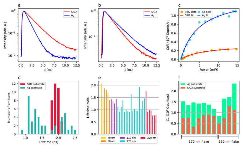
We also perform saturation measurements of multiple emitters on both substrates, by recording the count rate as a function of the laser power in cw regime. Figure 2c provides an example of such measurement, for the same emitter, either on substrate A (orange dots) or B (light blue dots). In this particular case, the change of substrate yielded a clear enhancement of the collection efficiency. The data are fitted using the power dependence of the count rate from a two-level system, , allowing to extract the high-power asymptote . The coupling between the incident laser and a given emitter can vary from sample A to sample B due to interference effects between the incident and the reflected laser beam. However, this would only affect and not the asymptote , which corresponds to a maximum population of the excited state, independently of the laser power needed to reach it. Thus, only depends on the emitter lifetime and on the collection efficiency, which also varies from sample A to B. Figure 2f presents for several emitters, before and after transfer. The enhancement of the collection efficiency by the Ag structure varies depending on the emitter, which can be attributed to the variety of flake thicknesses and vertical positions of the measured emitters, as we confirm in the following section devoted to numerical simulations.
III Numerical simulations
To gain quantitative insight into these experimental results, we perform numerical simulations using the finite difference time domain (FDTD) method. We use a point dipole source with in-plane orientation, given that the B-centers have a single dipole oriented in the basal plane [10]. The point dipole is located at a distance from the bottom of the flake (see figure 1). To closely match our experimental protocol, for each vertical position of the emitter, we calculate the ratio between the Purcell factor in both structures: . Experimentally, this ratio corresponds to the ratio between lifetimes and measured for a given emitter located at a given height . Figure 3 shows calculated for five flake thicknesses matching the experimentally investigated samples. In all cases, the Purcell factor diverges when vanishes, due to the proximity to the metal layer. For the three thinnest flakes, has a monotonic dependence on , allowing an unequivocal identification of the emitter position from the measured lifetimes and . In the case of the two thickest flakes in turn, oscillates for nm, and in some regions lies below 1, indicating a slight inhibition of the spontaneous emission. These oscillations originate from the varying coupling to the in-plane guided mode, as will be evidenced in the following section. For the 220 nm flake, we calculate the lowest value of to be 0.76. This value closely matches the highest inhibition of the spontaneous emission measured for a SPE in this flake (, see figure 2e). Given that our simulations model a purely radiative dipole (), this excellent agreement thus demonstrates that .

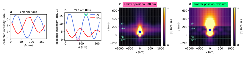
In the case of the 170 nm and 220 nm flakes, the Purcell factor alone does not allow a definite identification of the emitter position, since it is non-monotonic. Therefore, for the two thickest flakes, we also perform FDTD simulations to calculate the power radiated into a top objective of NA = 0.95, matching our experimental setup. Figure 4 shows the calculation results for the two crystals in configurations A and B. The collected intensity oscillates as a function of in all cases, due to a competition between in-plane and out-of-plane emission. This phenomenon is at the origin of the brightness disparities of SPEs in thick flakes observed in prior work [24]. Interestingly, the position of the nodes and antinodes is different on substrates A and B due to different boundary conditions. This leads to a position-dependent enhancement of the collection efficiency upon transfer from substrate A to B. The variation of the radiation pattern with is illustrated by the electric field profile shown on figure 4c and d, respectively at a minimum and at a maximum of the collection. In the former case, most of the light is emitted in the plane, while in the latter case, the light is directed to the top with a relatively low divergence (about 40∘ emission angle), which could be efficiently collected by an air objective of NA . This shows that the metal-dielectric structure constitutes a simple yet effective way to improve the photon collection. Simulations predict collection enhancement up to a factor 8, consistent with our experimental observations. Additionally, the oscillations of the collection enhancement as a function of the emitter position provides an additional information likely to lift the remaining uncertainty about the emitter positioning as inferred only by the Purcell factor.
IV Determination of emitter positions
In this section, we use a maximum likelihood estimation method to infer the emitter positions from the Purcell enhancement and, when necessary, the collection enhancement. We attribute to a measured physical quantity a Gaussian probability distribution function (PDF) , where is the theoretical (calculated) value of the parameter for a position , the measured value, and accounts for the experimental uncertainties. The likelihood function is defined as the joint PDF of all parameters , i.e. . Its maximum provides the most likely emitter position given the measured values of the physical quantities , and its width gives the associated confidence interval.
For the three thin flakes, we use a single parameter which is the Purcell enhancement , associated with the theoretical value . As expected, the associated likelihood function has in all cases a single maximum. This is however not the case for the 170 nm and 220 nm flakes due to the non-monotonicity of as visible on figure 3. For these two cases, we therefore use two parameters, namely the Purcell enhancement and the collection enhancement. Experimentally, the latter is evaluated through the ratio , where is the high power asymptote of the count rate measured in structure A (B). To illustrate the method, we focus on the example of a particular emitter of the 170 nm flake, whose characterization yields a Purcell factor of and a collection enhancement of . Figure 5a shows the single-parameter likelihood functions and associated with the Purcell enhancement and the collection enhancement, respectively. For this representative emitter, the Purcell enhancement is associated with two most likely positions (80 nm and 113 nm), as visible through the shape of (blue curve) and consistently with the simulation shown on figure 3. In turn, the collection efficiency is compatible with four positions, as evidenced by (orange curve). As a result, the (total) likelihood function has a single maximum, showing that cross-referencing these two observables has allowed to decide the most likely position, resulting in improved accuracy.
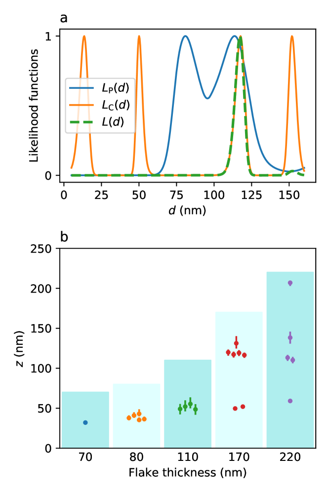
The results of the position estimation on the five samples are shown on figure 5b, where the dots represent the emitter vertical position, the error bars provide the associated confidence level, and the blue rectangle delimits the flakes in the vertical direction. In the three thin flakes, the emitters are found near the center of the flake. In the 170 nm flake, the emitters are also found rather far from the interfaces, and are grouped into two regions, with no emitter found around nm. As can be seen on figure 4a, this region corresponds to vanishing collection from the top, with predominant photon emission in the plane. Therefore, it cannot be concluded that there are no emitters with nm, since their emission would anyway not be efficiently detected by our setup. Similar considerations can be drawn for the thickest flake, which has two regions of vanishing upwards emission around nm and nm, where no emitters are found. The main general observation from the obtained distributions is that most emitters are found more than 30 nm away from the flake boundaries, at the exception of a single emitter on the 220 nm flake. We note that, unusually, the likelihood function of this particular emitter is not single-peaked and has a secondary maximum at position nm. We therefore cannot strictly exclude that this emitter is actually further away from the top interface.
A possible reason for obtaining estimated positions always far from the interfaces is that the SPEs might be unstable when created too close to the top surface. Indeed, the argument of a vanishing collection efficiency does not apply to SPEs near the interfaces, as clear from figure 4a and b, which shows sizable signal from dipoles located less than 30 nm away from the flake limits. This observation is consistent with the previously observed difficulty of creating stable B-centers in thin flakes [27], as well as the reported instability of other types of hBN quantum emitters, which exhibit blinking and bleaching for small thicknesses down to monolayers [3, 28]. However, for emitters near the underside, quenching effects due to the proximity of the Ag layer become significant [25, 26], so that no definitive conclusions concerning their absence or instability can be drawn from our experiment. To stabilize the emitters near the flake surface, potential mitigation strategies could include encapsulation in undoped hBN layers or other suitable materials.
V Conclusion
We have compared the emission properties of individual hBN color centers in two different planar photonic structures. We took benefit from dry transfer techniques, which allowed us to track individual emitters and study the influence of varying electromagnetic environment on their dynamics. Based on Purcell modification of their lifetime, we have estimated that their quantum efficiency is about unity. We have also inferred the distribution of their vertical positions – which is a subset of the possible locations of B-centers upon electron beam irradiation. We conclude that they are mostly located away from the flake interfaces, potentially due to a lower stability of SPEs close to the crystal boundaries. Finally, our work demonstrates a simple approach to boost the collection efficiency of quantum emitters in 2D materials, which does not involve demanding nanofabrication techniques.
VI Methods
Silver mirror fabrication
The metallic mirror is realized on a SiO2/Si substrate by Ag RF sputtering (Leybold Z400) on a 5 nm thick Ti adhesion layer, followed by depostion of 0.8 nm aluminum. The growth rates are 10 nm/min and 3.5 nm/min for Ag and Al, respectively. The Al layer naturally oxidizes when exposed to ambient atmosphere, thereby realizing a nm Al2O3 protective layer for the underneath Ag. XPS measurements ensure that all Al is oxidized, and that it covers hermetically the underlying Ag layer.
Exfoliation and transfer
Exfoliation is performed on substrate A from bulk crystals using commercial silicone elastomer films (Gel-Pak). The flake thicknesses are measured by atomic force microscopy. Transfer to substrate B is done using dry transfer [29] based on a glass slide with a home-made hemispherical polydimethylsiloxane stamp coated with polypropylene carbonate. The picking step from substrate A is done at 25 to 30 ∘C. The transfer is done by approaching the stamp at 40 ∘C and increasing the temperature to 80 to 100 ∘C after contact to release the flake on substrate B. The process ends with a cleaning step (acetone + isopropanol).
Optical measurements
Photoluminescence measurements are performed in a room-temperature confocal microscope using a NA air objective. The emitter are excited using a PicoQuant laser diode emitting at 405 nm, and working in either pulsed or cw regime. The photoluminescence signal is filtered using a bandpass fluorescence filter centered at 442 nm, and collected by two avalanche photodiodes in Hanbury Brown and Twiss configuration. Intensity autocorrelation is measured for all SPEs to ensure that we only consider individual emitters (i.e. ).
Numerical simulations
Numerical simulations are performed using Lumerical software, in 3D. The SPE is modeled by a point dipole with in-plane orientation. The complex refractive index of the Ag layer is measured by ellipsometry.
VII Acknowledgments
This work is supported by the French Agence Nationale de la Recherche (ANR) under reference ANR-21-CE47-0004-01 (ESCAPE project). The Authors acknowledge K. Watanabe and T. Taniguchi for providing hBN crystals, as well as J. Barjon and C. Arnold for many useful discussions.
References
- [1] Aharonovich, I.; Englund, D.; Toth, M. Solid-State Single-Photon Emitters. Nature Photon. 2016, 10, 631–641.
- [2] Wang, J.; Sciarrino, F.; Laing, A.; Thompson, M. G.. Integrated Photonic Quantum Technologies. Nat. Photonics 2020, 14, 273–284.
- [3] Tran, T. T.; Bray, K.; Ford, M. J.; Toth, M.; Aharonovich, I. Quantum emission from hexagonal boron nitride monolayers. Nat. Nanotechnol. 2016, 11, 37.
- [4] Bourrelier, R.; Meuret, S.; Tararan, A.; Stéphan, O.; Kociak, M.; Tizei, L. H. G.; Zobelli, A. Bright UV Single Photon Emission at Point Defects in h-BN. Nano Lett. 2016, 16, 4317.
- [5] Martínez, L. J.; Pelini, T.; Waselowski, V.; Maze, J. R.; Gil, B.; Cassabois, G.; Jacques, V. Efficient Single Photon Emission from a High-Purity Hexagonal Boron Nitride Crystal. Phys. Rev. B 2016, 94, 121405.
- [6] Schell, A. W.; Svedendahl, M.; Quidant, R. Quantum Emitters in Hexagonal Boron Nitride Have Spectrally Tunable Quantum Efficiency. Adv. Mater. 2018, 30, 1704237.
- [7] Nikolay, N.; Mendelson, N.; Özelci, E.; Sontheimer, B.; Böhm, F.; Kewes, G.; Toth, M.; Aharonovich, I.; Benson, O. Direct Measurement of Quantum Efficiency of Single-Photon Emitters in Hexagonal Boron Nitride. Optica 2019, 6, 1084.
- [8] Reimers, J. R.; Shen, J.; Kianinia, M.; Bradac, C.; Aharonovich, I.; Ford, M. J.; Piecuch, P. Photoluminescence, Photophysics, and Photochemistry of the V Defect in Hexagonal Boron Nitride. Phys. Rev. B 2020, 102, 144105.
- [9] Shevitski, B.; Gilbert, S. M.; Chen, C. T.; Kastl, C.; Barnard, E. S.; Wong, E.; Ogletree, D. F.; Watanabe, K.; Taniguchi, T.; Zettl, A.; Aloni, S. Blue-Light-Emitting Color Centers in High-Quality Hexagonal Boron Nitride. Phys. Rev. B 2019, 100, 155419.
- [10] Fournier, C.; Plaud, A.; Roux, S.; Pierret, A.; Rosticher, M.; Watanabe, K.; Taniguchi, T.; Buil, S.; Quélin, X.; Barjon, J.; Hermier, J.-P.; Delteil, A. Position-Controlled Quantum Emitters with Reproducible Emission Wavelength in Hexagonal Boron Nitride. Nat. Commun. 2021, 12, 3779.
- [11] Gale, A.; Li, C.; Chen, Y.; Watanabe, K.; Taniguchi, T.; Aharonovich, I.; Toth, M. Site-Specific Fabrication of Blue Quantum Emitters in Hexagonal Boron Nitride. ACS Photonics 2022, 9, 2170.
- [12] Horder, J.; White, S. J. U.; Gale, A.; Li, C.; Watanabe, K.; Taniguchi, T.; Kianinia, M.; Aharonovich, I.; Toth, M. Coherence Properties of Electron-Beam-Activated Emitters in Hexagonal Boron Nitride Under Resonant Excitation. Phys. Rev. Appl. 2022, 18, 064021.
- [13] Fournier, C.; Roux, S.; Watanabe, K.; Taniguchi, T.; Buil, S.; Barjon, J.; Hermier, J.-P.; Delteil, A. Two-Photon Interference from a Quantum Emitter in Hexagonal Boron Nitride. Phys. Rev. Appl. 2023, 19, L041003.
- [14] Fournier, C.; Watanabe, K.; Taniguchi, T.; Buil, S.; Barjon, J.; Hermier, J.-P.; Delteil, A. Investigating the Fast Spectral Diffusion of a Quantum Emitter in hBN Using Resonant Excitation and Photon Correlations. Phys. Rev. B 2023, 107, 195304.
- [15] Gérard, D.; Rosticher, M.; Watanabe, K.; Taniguchi, T.; Barjon, J.; Buil, S.; Hermier, J.-P.; Delteil, A. Top-Down Integration of a hBN Quantum Emitter in a Monolithic Photonic Waveguide. Appl. Phys. Lett. 2023, 122, 264001.
- [16] Spencer, L.; Horder, J.; Kim, S.; Toth, M.; Aharonovich, I. Monolithic Integration of Single Quantum Emitters in hBN Bullseye Cavities. ACS Photon. 2023, 10, 4417.
- [17] Drexhage, K. H. Influence of a Dielectric Interface on Fluorescence Decay Time. J. Lumin. 1970, 1, 693.
- [18] Tews, K.-H.; Inacker, O.; Kuhn, H. Variation of the Luminescence Lifetime of a Molecule Near an Interface Between Differently Polarizable Dielectrics. Nature 1970, 228, 276.
- [19] Kunz, R. E.; Lukosz, W. Changes in Fluorescence Lifetimes Induced by Variable Optical Environments. Phys. Rev. B 1980, 21, 4814.
- [20] Brokmann, X.; Coolen, L.; Dahan, M.; Hermier, J. P. Measurement of the Radiative and Nonradiative Decay Rates of Single CdSe Nanocrystals Through a Controlled Modification of Their Spontaneous Emission. Phys. Rev. Lett. 2004, 93, 107403.
- [21] Tran, T. T.; Wang, D.; Xu, Z.-Q.; Yang, A.; Toth, M.; Odom, T. W.; Aharonovich, I. Deterministic Coupling of Quantum Emitters in 2D Materials to Plasmonic Nanocavity Arrays. Nano Lett. 2017, 17, 2634.
- [22] Dowran, M.; Butler, A.; Lamichhane, S.; Erickson, A.; Kilic, U.; Liou, S.-H.; Argyropoulos, C.; Laraoui, A. Plasmon Enhanced Quantum Properties of Single Photon Emitters with Hybrid Hexagonal Boron Nitride Silver Nanocube Systems. Adv. Opt. Mater. 2023, 11, 2300392.
- [23] Taniguchi, T.; Watanabe, K. Synthesis of High-Purity Boron Nitride Single Crystals Under High Pressure by Using Ba–BN Solvent. J. Cryst. Growth 2007, 303, 525-529.
- [24] Roux, S.; Fournier, C.; Watanabe, K.; Taniguchi, T.; Hermier, J.-P.; Barjon, J.; Delteil, A. Cathodoluminescence Monitoring of Quantum Emitter Activation in Hexagonal Boron Nitride. Appl. Phys. Lett. 2022, 121, 184002.
- [25] Anger, P.; Bharadwaj, P.; Novotny, L. Enhancement and Quenching of Single-Molecule Fluorescence. Phys. Rev. Lett. 2006, 96, 113002.
- [26] Vion, C.; Spinicelli, P.; Coolen, L.; Schwob, C.; Frigerio, J.-M.; Hermier, J.-P.; Maître, A. Controlled Modification of Single Colloidal CdSe/ZnS Nanocrystal Fluorescence Through Interactions with a Gold Surface. Opt. Expr. 2010, 18, 7440.
- [27] Nedić, S.; Yamamura, K.; Gale, A.; Aharonovich, I.; Toth, M. Electron Beam Restructuring of Quantum Emitters in Hexagonal Boron Nitride. Adv. Opt. Mater. 2024, 2400908.
- [28] Stern, H. L.; Wang, R.; Fan, Y.; Mizuta, R.; Stewart, J. C.; Needham, L.-M.; Roberts, T. D.; Wai, R.; Ginsberg, N. S.; Klenerman, D.; Hofmann, S.; Lee, S. F. Spectrally Resolved Photodynamics of Individual Emitters in Large-Area Monolayers of Hexagonal Boron Nitride. ACS Nano 2019, 13, 4538.
- [29] Wang, L.; Meric, I.; Huang, P. Y.; Gao, Q.; Gao, Y.; Tran, H.; Taniguchi, T.; Watanabe, K.; Campos, L. M.; Muller, D. A.; Guo, J.; Kim, P.; Hone, J.; Shepard, K. L.; Dean, C. R. One-Dimensional Electrical Contact to a Two-Dimensional Material. Science 2013, 342, 614.