Designing single and degenerate flat bands in the Kagome lattice with long-range hopping
Abstract
We investigate the electronic structure of the kagome lattice model with first, second, and two kinds of third nearest-neighbor hoppings. We reveal that by tuning the third nearest-neighbor hoppings, not only single flat band but also degenerate flat band can be created on the -M line. We provide the detailed conditions to realize them. The coexistence of these bands can be almost realized near the fundamental band gap in graphene with triangular defects in a superhoneycomb arrangement. Our results strongly indicate that long-range electron hopping has a new possibility for designing electronic structures.
Controlling the electronic structure is an important issue to improve materials properties of periodic systems. Diversity of constituent elements and structures leads to various electronic structures. For example, flat band is known to significantly contribute to interesting electronic properties such as superconductivity [1, 2, 3, 4, 5, 6], ferromegnetism [7, 8, 9, 10, 11, 12, 13] and topological phenomena [14, 15, 16, 17, 18, 19, 20, 21, 22, 23, 24, 25, 26, 27]. So far, various flat-band models [28, 29, 30, 31, 32, 33, 34, 35, 36, 37, 38, 39, 40, 41, 42], e.g., square lattice [8] and kagome lattice [31, 36] have been studied. In general, long-range hoppings break the band’s flatness, but some research shows how to maintain a flat band with the addition of next-nearest neighbor hopping[36, 41]. Exploration of materials [43, 44, 45, 46, 47, 48, 49, 50, 41, 42] which realize flat-band model is also an important issue. Recently, data science has been applied to explore flat-band materials more efficiently [51].
Another intriguing property in electronic structure is degenerate band. Degeneracy in band dispersion such as Dirac cone and nodal line has attracted much attention since they trigger non-trivial physical phenomena such as the appearance of drumhead surface state and huge anomalous Nernst effect [52, 53]. Therefore, not only single flat band but also degenerate flat band is worth studying. In general, degenerate band has been studied in terms of structure symmetry [54, 55, 56, 57, 58], so whether degenerate flat band can be designed without changing symmetry, is an interesting question for flat-band model and flat-band materials design.
In this letter, we study the kagome lattice model including long-range hopping. We reveal that not only single flat band but also degenerate flat band appears by introducing long range hopping, i.e., the third nearest neighbor hopping, under certain conditions. To the best of our knowledge, method for designing degenerate flat band has never been proposed theoretically in the kagome lattice. We also show that the above conditions are realized in graphene with triangular defects by extending the distance between defects.
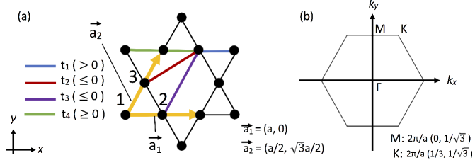
We focus on the kagome lattice with not only the nearest neighbor electron hopping () but also the second () and the third ( and ) nearest neighbor electron hoppings as shown in Fig. 1(a). Here, let us define P as the point which internally divide the -M line (Fig. 1(b)) into . The Bloch Hamiltonian at P of this model can be expressed as
| (1) |
It is to be noted that components of denotes electron hopping between sublattices and in Fig. 1(a). The detailed derivation of is shown in the Supplemental Material No. 2 [59]. From this , we can obtain the Hamiltonians at the M point (), the middle point of -M line () and the point ().
We use these three Hamiltonians to study the conditions of which realize single flat band or degenerate flat bands on the -M line hereafter.
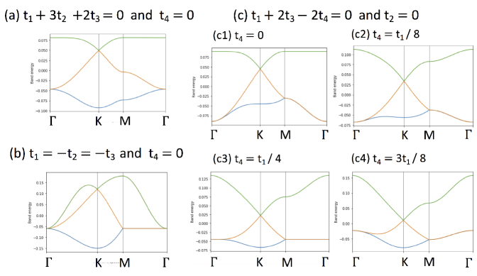
Figure 2 (a) shows the electronic structure for and , obtained by diagonalizing eq. (1). We see that a single flat band appears between M and . We also find another condition to realize flat band. When and are satisfied, degenerate flat band appears, as shown in Fig. 2(b). It is to be noted that degenerate flat band cannot be designed when only and are considered. This result strongly indicates that long-range electron hopping plays an important role in creating various types of electronic structures. In addition, the degenerate flat band by using long range hopping is realized without changing system symmetry.
Figure 2(c1) is the result for the special case of (a), i.e., and . We find a single flat band and degenerate (but not flat) band between M and . As we increase with keeping , the band width of the degenerate band decreases, and becomes flat when , then turns to increase (Fig. 2(c2)-(c4)).
To understand the above results, we first focus on the case of . The conditions that the flat band appears can be derived by focusing on eigenvalues of , and . The detailed derivations are given in the Supplemental Material No. 3A and No. 3B [59]. The single flat band in Fig. 2(a) is dispersive in the case of kagome lattice with only as shown in Fig. S1 of the Supplemental Material [59]. By introducing and appropriately, this dispersive band loses dispersion between line and between part of line. Appearing the degenerate flat band between line in Fig, 2(b) is interesting, but it is hard to to realize in real materials due to the condition of . It would be very difficult to have the same absolute value for and . However, by also introducing , degenerate flat band between line can be designed under more realistic condition, as will be discussed later.
Secondly, we focus on the kagome lattice considering and . As shown in Fig. 2(c) and Fig. S3 (Supplemental Material [59]), degenerate band always appears between line under the condition of (i) and , or (ii) and . The detailed derivations of these condition are shown in the Supplemental Material No. 3(c) [59]. In this main text, we discuss (i) and case. The eigenvalue of the degenerate band is , so the bandwidth of degenerate band is . Therefore, this bandwidth monotonically decreases with () and increases with (). When , the degenerate band becomes flat as shown in Fig. 2(c3). Hence, smaller than plays a crucial role in flattering degenerate band between line. The condition for degenerate flat band is (Fig. 2(c3)), which is more realistic than (Fig. 2(b)).
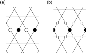
Here, let us discuss the interference effect and the real space picture in the case of Fig. 2(2c) where degenerate flat band between line appears. Firstly, in the case of the kagome-lattice model with only , any kinds of Kohn-Sham wave function in flat band can be constructed by linear combination of localized molecular orbitals. This molecular orbital is localized in real space due to quantum interference effect of hopping and atomic orbitals’ phases. Next, in our present study, degenerate flat band appears between line as shown in Fig. 2(2c). Similar to the kagome-lattice model with only , we can design any kinds of Kohn-Sham wave function between line by linear combination of localized doubly degenerate polymer orbitals. These polymer orbitals are shown in Fig. 3. The polymer orbital shown in Fig. 3(a), is the eigenstate in the case of the kagome-lattice model with only , and the linear combination of it constructs flat band between line. This orbital is also the eigenstate when we consider the long range hopping and due to interference effect of them. On the other hand, the orbital shown in Fig. 3(b), is not the eigenstate in the case of the kagome-lattice model with only . When the state at the point is designed by the linear combination of this orbital, this state can be an eigenstate degenerated with the polymer orbital shown in Fig. 3(a), but degeneracy does not occur at the general point between line and the energy dispersion is not flat. In the case of the kagome-lattice model with , and , the polymer orbital shown in Fig. 3(b) is the eigenstate and it has the same energy () as the polymer orbital shown in Fig. 3(a). Considering the fact that the irreducible representations of these wavefunctions of the polymers are different (Fig. 3), the degeneracy between line in Fig. 2(2c) is not protected by two dimensional representation. We find that two properties, degeneracy and localization, are realized by interference effect of electron hopping.
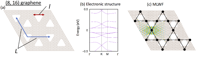
Next, we discuss materials realization of the flat band. The electronic structure of the kagome-lattice model with , with and (Fig. 2(c)), can be nearly realized in graphene with triangular defects in a superhoneycomb arrangement, which is called graphene in our previous paper [63] (Fig 4(a)). In the caption of Fig 4, the definitions of and are explained. In Fig 4(b), and Figs. S5(a) and S6(a) [59], the electronic structures of , and graphenes obtained by the first-principle calculations are shown, respectively. We show the details of the ab initio calculation in the Supplemental Material [59]. In the discussion that follows, we focus on the first lowest-unoccupied (LU) and the second LU and the third LU bands. As increases, the shape of these bands becomes similar to that shown in Fig. 2(c1). Hence, we expect that the kagome-lattice model with , where and , is nearly realized when is large.
| (eV) | (eV) | (eV) | (eV) | (eV) | |
|---|---|---|---|---|---|
| 10 | 0.031 | -0.021 | -0.0099 | 0.00038 | 0.010 |
| 13 | 0.033 | -0.0069 | -0.013 | 0.0018 | 0.0034 |
| 16 | 0.029 | -0.0028 | -0.013 | 0.0028 | -0.0026 |
We can confirm it by constructing the maximally localized Wannier functions (MLWFs) from these bands. The WLWF has a Wannier center in the center of the graphene nanoribbon, forming a Kagome lattice(Fig 4(c)). The MLWF originates from the hybridized two edge states of the nanoribbon. In Table 1, the calculated of graphenes ( and 16) are shown. Interestingly, the value of does not decrease with increasing while the value of decreases sharply with . The MLWF extends outside of the subribbon part, and due to this, value is nonzero for large . We find that , , and results in and for large case.
Let us focus on the electronic structure of graphene shown in Fig. 4. On the line, the nearly single flat band (bandwidth: 0.016 eV) and the degenerate flat band (bandwidth: 0.024 eV and 0.034 eV) coexist. In the case of graphene, (Table 1) holds, so plays a role in decreasing the degenerate bandwidth. Actually, if we do not consider , the degenerate bandwidth is eV, which is larger than that of the first-principles calculation. On the other hand, plays a role in increasing the single bandwidth (, Fig. S2 of the Supplemental Material [59]). However, due to very small value ( eV (Table. 1)), the single band is nearly flat.
In this letter, we have studied the electronic structure of the kagome lattice with the first (), the second () and the third () nearest neighbor hoppings. It is found that not only single flat band but also degenerate flat band on the line can be designed by introducing and appropriately. It is realized in graphene with triangular defects in a superhoneycomb arrangement. By extending distance between defects, approaches the condition for appearing degenerate flat band, and then, nearly single flat and nearly degenerate band coexist on the line.
Acknowledgements.
YT acknowledge the financial support from JST SPRING, Grant Number JPMJSP2106, and Tokyo Tech Academy for Convergence of Materials and Informatics (TAC-MI). Numerical calculations were done at the Supercomputer Center of the Institute for Solid State Physics, The University at Tokyo; at the Center for Computational Materials Science, Institute for Materials Research, Tohoku University for the use of MASAMUNE-IER; and at the Global Scientific Information and Computing Center of the Tokyo Institute of Technology.References
- Imada and Kohno [2000] M. Imada and M. Kohno, Superconductivity from flat dispersion designed in doped mott insulators, Physical Review Letters 84, 143 (2000).
- Kuroki et al. [2005] K. Kuroki, T. Higashida, and R. Arita, High-t c superconductivity due to coexisting wide and narrow bands: A fluctuation exchange study of the hubbard ladder as a test case, Physical Review B 72, 212509 (2005).
- Kobayashi et al. [2016] K. Kobayashi, M. Okumura, S. Yamada, M. Machida, and H. Aoki, Superconductivity in repulsively interacting fermions on a diamond chain: Flat-band-induced pairing, Physical Review B 94, 214501 (2016).
- Matsumoto et al. [2018] K. Matsumoto, D. Ogura, and K. Kuroki, Wide applicability of high-t c pairing originating from coexisting wide and incipient narrow bands in quasi-one-dimensional systems, Physical Review B 97, 014516 (2018).
- Mondaini et al. [2018] R. Mondaini, G. G. Batrouni, and B. Grémaud, Pairing and superconductivity in the flat band: Creutz lattice, Physical Review B 98, 155142 (2018).
- Aoki [2020] H. Aoki, Theoretical possibilities for flat band superconductivity, Journal of Superconductivity and Novel Magnetism 33, 2341 (2020).
- Mielke [1991] A. Mielke, Ferromagnetism in the hubbard model on line graphs and further considerations, Journal of Physics A: Mathematical and General 24, 3311 (1991).
- Tasaki [1992] H. Tasaki, Ferromagnetism in the hubbard models with degenerate single-electron ground states, Physical review letters 69, 1608 (1992).
- Mielke and Tasaki [1993] A. Mielke and H. Tasaki, Ferromagnetism in the hubbard model: Examples from models with degenerate single-electron ground states, Communications in mathematical physics 158, 341 (1993).
- Kusakabe and Aoki [1994] K. Kusakabe and H. Aoki, Ferromagnetic spin-wave theory in the multiband hubbard model having a flat band, Physical review letters 72, 144 (1994).
- Ramirez [1994] A. Ramirez, Strongly geometrically frustrated magnets, Annual Review of Materials Science 24, 453 (1994).
- Tasaki [1998] H. Tasaki, From nagaoka’s ferromagnetism to flat-band ferromagnetism and beyond: an introduction to ferromagnetism in the hubbard model, Progress of theoretical physics 99, 489 (1998).
- Tamura and Katsura [2019] K. Tamura and H. Katsura, Ferromagnetism in the su (n) hubbard model with a nearly flat band, Physical Review B 100, 214423 (2019).
- Aoki et al. [1996] H. Aoki, M. Ando, and H. Matsumura, Hofstadter butterflies for flat bands, Physical Review B 54, R17296 (1996).
- Vidal et al. [1998] J. Vidal, R. Mosseri, and B. Douçot, Aharonov-bohm cages in two-dimensional structures, Physical review letters 81, 5888 (1998).
- Guo and Franz [2009] H.-M. Guo and M. Franz, Topological insulator on the kagome lattice, Physical Review B 80, 113102 (2009).
- Weeks and Franz [2010] C. Weeks and M. Franz, Topological insulators on the lieb and perovskite lattices, Physical Review B 82, 085310 (2010).
- Green et al. [2010] D. Green, L. Santos, and C. Chamon, Isolated flat bands and spin-1 conical bands in two-dimensional lattices, Physical Review B 82, 075104 (2010).
- Tang et al. [2011] E. Tang, J.-W. Mei, and X.-G. Wen, High-temperature fractional quantum hall states, Physical review letters 106, 236802 (2011).
- Sun et al. [2011] K. Sun, Z. Gu, H. Katsura, and S. D. Sarma, Nearly flatbands with nontrivial topology, Physical review letters 106, 236803 (2011).
- Neupert et al. [2011] T. Neupert, L. Santos, C. Chamon, and C. Mudry, Fractional quantum hall states at zero magnetic field, Physical review letters 106, 236804 (2011).
- Wang and Ran [2011] F. Wang and Y. Ran, Nearly flat band with chern number c= 2 on the dice lattice, Physical Review B 84, 241103 (2011).
- Liu et al. [2012] Z. Liu, E. J. Bergholtz, H. Fan, and A. M. Läuchli, Fractional chern insulators in topological flat bands with higher chern number, Physical review letters 109, 186805 (2012).
- Rhim and Yang [2019] J.-W. Rhim and B.-J. Yang, Classification of flat bands according to the band-crossing singularity of bloch wave functions, Physical Review B 99, 045107 (2019).
- Mizoguchi and Hatsugai [2020] T. Mizoguchi and Y. Hatsugai, Systematic construction of topological flat-band models by molecular-orbital representation, Physical Review B 101, 235125 (2020).
- Kuno [2020] Y. Kuno, Extended flat band, entanglement, and topological properties in a creutz ladder, Physical Review B 101, 184112 (2020).
- Kuno et al. [2020] Y. Kuno, T. Mizoguchi, and Y. Hatsugai, Interaction-induced doublons and embedded topological subspace in a complete flat-band system, Physical Review A 102, 063325 (2020).
- Sutherland [1986] B. Sutherland, Localization of electronic wave functions due to local topology, Physical Review B 34, 5208 (1986).
- Shima and Aoki [1993] N. Shima and H. Aoki, Electronic structure of super-honeycomb systems: A peculiar realization of semimetal/semiconductor classes and ferromagnetism, Physical review letters 71, 4389 (1993).
- Miyahara et al. [2005] S. Miyahara, K. Kubo, H. Ono, Y. Shimomura, and N. Furukawa, Flat-bands on partial line graphs–systematic method for generating flat-band lattice structures–, Journal of the Physical Society of Japan 74, 1918 (2005).
- Bergman et al. [2008] D. L. Bergman, C. Wu, and L. Balents, Band touching from real-space topology in frustrated hopping models, Physical Review B 78, 125104 (2008).
- Hatsugai and Maruyama [2011] Y. Hatsugai and I. Maruyama, Zq topological invariants for polyacetylene, kagome and pyrochlore lattices, Europhysics Letters 95, 20003 (2011).
- Misumi and Aoki [2017] T. Misumi and H. Aoki, New class of flat-band models on tetragonal and hexagonal lattices: Gapped versus crossing flat bands, Physical Review B 96, 155137 (2017).
- Ramachandran et al. [2017] A. Ramachandran, A. Andreanov, and S. Flach, Chiral flat bands: Existence, engineering, and stability, Physical Review B 96, 161104 (2017).
- Maimaiti et al. [2019] W. Maimaiti, S. Flach, and A. Andreanov, Universal d= 1 flat band generator from compact localized states, Physical Review B 99, 125129 (2019).
- Mizoguchi and Udagawa [2019] T. Mizoguchi and M. Udagawa, Flat-band engineering in tight-binding models: Beyond the nearest-neighbor hopping, Physical Review B 99, 235118 (2019).
- Mizoguchi and Hatsugai [2019] T. Mizoguchi and Y. Hatsugai, Molecular-orbital representation of generic flat-band models, Europhysics Letters 127, 47001 (2019).
- Maimaiti et al. [2021] W. Maimaiti, A. Andreanov, and S. Flach, Flat-band generator in two dimensions, Physical Review B 103, 165116 (2021).
- Mizoguchi et al. [2021a] T. Mizoguchi, Y. Kuno, and Y. Hatsugai, Flat band, spin-1 dirac cone, and hofstadter diagram in the fermionic square kagome model, Physical Review B 104, 035161 (2021a).
- Mizoguchi et al. [2021b] T. Mizoguchi, H. Katsura, I. Maruyama, and Y. Hatsugai, Flat-band solutions in d-dimensional decorated diamond and pyrochlore lattices: Reduction to molecular problem, Physical Review B 104, 035155 (2021b).
- Mizoguchi et al. [2023] T. Mizoguchi, Y. Gao, M. Maruyama, Y. Hatsugai, and S. Okada, Unconventional gapless semiconductor in an extended martini lattice in covalent honeycomb materials, Physical Review B 107, L121301 (2023).
- Kim and Liu [2023] D. Kim and F. Liu, Realization of flat bands by lattice intercalation in kagome metals, Physical Review B 107, 205130 (2023).
- Yamada et al. [2016] M. G. Yamada, T. Soejima, N. Tsuji, D. Hirai, M. Dincă, and H. Aoki, First-principles design of a half-filled flat band of the kagome lattice in two-dimensional metal-organic frameworks, Physical Review B 94, 081102 (2016).
- Hase et al. [2018] I. Hase, T. Yanagisawa, Y. Aiura, and K. Kawashima, Possibility of flat-band ferromagnetism in hole-doped pyrochlore oxides sn 2 nb 2 o 7 and sn 2 ta 2 o 7, Physical review letters 120, 196401 (2018).
- Maruyama et al. [2016] M. Maruyama, N. T. Cuong, and S. Okada, Coexistence of dirac cones and kagome flat bands in a porous graphene, Carbon 109, 755 (2016).
- Maruyama and Okada [2017] M. Maruyama and S. Okada, Interplay between the kagome flat band and the dirac cone in porous graphitic networks, Carbon 125, 530 (2017).
- Lee et al. [2019] C.-C. Lee, A. Fleurence, Y. Yamada-Takamura, and T. Ozaki, Hidden mechanism for embedding the flat bands of lieb, kagome, and checkerboard lattices in other structures, Physical Review B 100, 045150 (2019).
- Kang et al. [2020a] M. Kang, S. Fang, L. Ye, H. C. Po, J. Denlinger, C. Jozwiak, A. Bostwick, E. Rotenberg, E. Kaxiras, J. G. Checkelsky, et al., Topological flat bands in frustrated kagome lattice cosn, Nature communications 11, 4004 (2020a).
- Kang et al. [2020b] M. Kang, L. Ye, S. Fang, J.-S. You, A. Levitan, M. Han, J. I. Facio, C. Jozwiak, A. Bostwick, E. Rotenberg, et al., Dirac fermions and flat bands in the ideal kagome metal fesn, Nature materials 19, 163 (2020b).
- Fleurence et al. [2020] A. Fleurence, C.-C. Lee, R. Friedlein, Y. Fukaya, S. Yoshimoto, K. Mukai, H. Yamane, N. Kosugi, J. Yoshinobu, T. Ozaki, et al., Emergence of nearly flat bands through a kagome lattice embedded in an epitaxial two-dimensional ge layer with a bitriangular structure, Physical Review B 102, 201102 (2020).
- Bhattacharya et al. [2023] A. Bhattacharya, I. Timokhin, R. Chatterjee, Q. Yang, and A. Mishchenko, Deep learning approach to genome of two-dimensional materials with flat electronic bands, npj Computational Materials 9, 101 (2023).
- Sakai et al. [2020] A. Sakai, S. Minami, T. Koretsune, T. Chen, T. Higo, Y. Wang, T. Nomoto, M. Hirayama, S. Miwa, D. Nishio-Hamane, et al., Iron-based binary ferromagnets for transverse thermoelectric conversion, Nature 581, 53 (2020).
- Chen et al. [2022] T. Chen, S. Minami, A. Sakai, Y. Wang, Z. Feng, T. Nomoto, M. Hirayama, R. Ishii, T. Koretsune, R. Arita, et al., Large anomalous nernst effect and nodal plane in an iron-based kagome ferromagnet, Science advances 8, eabk1480 (2022).
- Young and Kane [2015] S. M. Young and C. L. Kane, Dirac semimetals in two dimensions, Physical review letters 115, 126803 (2015).
- Wieder et al. [2016] B. J. Wieder, Y. Kim, A. Rappe, and C. Kane, Double dirac semimetals in three dimensions, Physical review letters 116, 186402 (2016).
- Takahashi et al. [2017] R. Takahashi, M. Hirayama, and S. Murakami, Spinless hourglass nodal-line semimetals, Physical Review B 96, 155206 (2017).
- Yang et al. [2017] B.-J. Yang, T. A. Bojesen, T. Morimoto, and A. Furusaki, Topological semimetals protected by off-centered symmetries in nonsymmorphic crystals, Physical Review B 95, 075135 (2017).
- Zhang et al. [2019] T. Zhang, Y. Jiang, Z. Song, H. Huang, Y. He, Z. Fang, H. Weng, and C. Fang, Catalogue of topological electronic materials, Nature 566, 475 (2019).
- [59] See Supplemental Materials for the electronic structure of kagome-lattice model with , the detailed derivation of , the detailed derivation of to design single flat band and degenerate flat band between line, the calculation mathods and the calculation results of electronic structure, maximally localized Wannier function (MLWF), and optical conductivity.
- [60] PythTB, http://physics.rutgers.edu/pythtb/.
- Momma and Izumi [2008] K. Momma and F. Izumi, Vesta: a three-dimensional visualization system for electronic and structural analysis, Journal of Applied crystallography 41, 653 (2008).
- Giannozzi et al. [2009] P. Giannozzi, S. Baroni, N. Bonini, M. Calandra, R. Car, C. Cavazzoni, D. Ceresoli, G. L. Chiarotti, M. Cococcioni, I. Dabo, et al., Quantum espresso: a modular and open-source software project for quantum simulations of materials, Journal of physics: Condensed matter 21, 395502 (2009).
- Taguchi et al. [2023] Y. Taguchi, M. Toyoda, and S. Saito, Electronic properties of graphene with triangular defects in a superhoneycomb arrangement: A first-principles study, Physical Review B 107, 235418 (2023).