Automated and Holistic Co-design of Neural Networks and ASICs for Enabling In-Pixel Intelligence
Abstract
Extreme edge-AI systems, such as those in readout ASICs for radiation detection, must operate under stringent hardware constraints such as micron-level dimensions, sub-milliwatt power, and nanosecond-scale speed while providing clear accuracy advantages over traditional architectures. Finding ideal solutions means identifying optimal AI and ASIC design choices from a design space that has explosively expanded during the merger of these domains, creating non-trivial couplings which together act upon a small set of solutions as constraints tighten. It is impractical, if not impossible, to manually determine ideal choices among possibilities that easily exceed billions even in small-size problems. Existing methods to bridge this gap have leveraged theoretical understanding of hardware to create proxies for key metrics such as ASIC area and power and used them in neural architecture search. However, the assumptions made in computing such theoretical metrics are too idealized to provide sufficient guidance during the difficult search for a practical implementation. Meanwhile, theoretical estimates for many other crucial metrics (like delay) do not even exist and are similarly variable, dependent on parameters of the process design kit (PDK). To address these challenges, we present a study that employs intelligent search using multi-objective Bayesian optimization, integrating both neural network search and ASIC synthesis in the loop. This approach provides reliable feedback on the collective impact of all cross-domain design choices. We showcase the effectiveness of our approach by finding several Pareto-optimal design choices for effective and efficient neural networks that perform real-time feature extraction from input pulses within the individual pixels of a readout ASIC.
1 Introduction and Motivation
Real-time edge-AI systems are designed for inference at the edge of computing hardware, where data is generated, and are crucial for applications requiring swift detection, inference, and decision-making [22, 26, 39]. These systems must be adequately reliable while operating within stringent resource constraints, including limited area, power, and latency. Their design complexity is amplified by the numerous design choices available in both the AI and hardware spaces, the complex interactions between them, and their combined effect on the deployment feasibility in real-world applications [25].
Tackling the stringent requirements for extreme edge-AI systems has spurred innovations in AI models, hardware, and their co-design. In AI design, research has concentrated on model compression techniques such as quantization and pruning [23, 17] that enhance computational efficiency without detrimentally compromising accuracy. Similarly, innovations have emerged in AI accelerators customized for these AI models and their implementation on field-programmable gate arrays (FPGAs) [13, 38] and application-specific integrated circuits (ASICs) [20, 32]. The co-design approach has taken this process further by simultaneously considering design choices from both AI and hardware perspectives to find the best solution for both domains [5, 40].
This paper focuses on the co-design approach to addressing the challenges of extreme edge-AI systems. A significant challenge in co-design is the exponential growth in design choices and the substantial compute costs required to quantify its impact on design objectives. Automated searches with advanced algorithms like Bayesian optimization [34, 37] and reinforcement learning [1, 21] have shown promise in navigating this complex co-optimization space but remain too expensive to be practical for most applications, especially when quantifying the costly hardware objectives. Some progress has been made using theory-guided approximations to model hardware objectives [9, 7], but actual implementations often deviate significantly from these estimates, leading to sub-optimal or infeasible designs. While improving the accuracy of these estimates is crucial, it is often insufficient due to the unique and intricate nature of more practical hardware objectives for which theoretical estimates are not available.
Many scientific applications would benefit from fast, low-latency machine learning, including event reconstruction and triggering in particle accelerators, denoising of gravitational wave detectors, and real-time monitoring and control of plasma dynamics [15, 10]. ASICs represent a natural progression from the success of FPGA-based AI accelerators in such scientific applications. Unlike other specialized hardware, ASICs offer a unique combination of efficiency, area, and power optimization, enabling them to operate under the extreme conditions of edge computing and even advancing AI to pixel-level processing in devices such as radiation detectors [27, 29, 28, 24]. Despite these advantages, the field has remained relatively unexplored due to the high development costs, the need for close interdisciplinary collaboration with highly specialized hardware design domains - often lacking in academic and scientific settings - and the paucity of consumer-available options. However, the growing availability of open-source tools, increased support from government initiatives, and heightened scientific interest in advancing efficient AI has created a more feasible ecosystem for AI-ASIC co-design.
The AI-ASIC co-design environment presents more constraints than those typically encountered with AI accelerators and FPGAs. While this adds complexity, it also narrows the design space, enabling a more feasible approach for holistic integration, which is often challenging in broader settings. In this study, we embraced this unique context by holistically integrating design choices across the AI and ASIC domains. Instead of relying on theoretical estimates, our approach utilizes direct metrics obtained from hardware synthesis, incorporating these insights into a fully automated pipeline using multi-objective Bayesian optimization. This method allows us to consider more practical and necessary hardware objectives. We demonstrate the effectiveness of our approach on a scientific application, namely the design of on-chip neural networks for feature extraction from amplified charge pulses [28]. Such pulses, which are produced by readout ASICs designed for radiation sensing, encode information on the energy, direction of arrival, and identity of particles observed in high-energy physics experiments [33].
The main contributions of this work are as follows:
-
•
Realistic Estimates and Practicality: We incorporate more accurate estimates of design objectives in our optimization process to increase the likelihood of achieving designs that are both optimal and feasible.
-
•
Holistic Co-design integration: We expand on the usual co-design choices, such as the neural network architectures and quantization strategies, to also simultaneously consider ASIC synthesis strategies, thus enabling a more comprehensive search for practical designs.
-
•
Diversity of Co-design Objectives: We also expand our design objectives to include practically useful metrics such as the time delay of the circuit implementation, in addition to traditional optimization goals like accuracy, area, and power.
-
•
Open-source automation tool We provide the scientific community with an automated pipeline that utilizes fully open-source tools from both AI and ASIC domains. We also make data from thousands of ASIC synthesis runs available for further research.
Existing applications of AI algorithms in radiation detection are focused on offline data analysis, such as for event clustering and track reconstruction [3, 4]. These algorithms are generally implemented on graphics processing units (GPUs), which offer reconfigurability at the cost of non-deterministic latency and low energy efficiency. Thus, they are unsuitable for emerging applications, such as real-time denoising, that require online operation of the AI algorithms. The hardware platform of choice for such real-time applications has traditionally been FPGAs, which combine bit-level reconfigurability with deterministic latency. However, the energy efficiency of FPGAs, as measured using a suitable metric such as energy-delay product (EDP), is generally higher than that of GPUs but suffers from the significant overhead required to support the programming fabric. Thus, recent work has proposed AI accelerators implemented on the “edge” close to the data source, i.e., within the readout ASICs used for amplification and conditioning of charge waveforms [11, 28]. Such ASIC implementations offer significantly higher energy efficiency than FPGAs while also allowing the design to be optimized for the extreme environmental conditions (e.g., cryogenic or high-radiation) often encountered in near-detector environments. However, these advantages come at the cost of limited post-fabrication reconfigurability. Given the limited power, area, and computational resources of the readout ASICs, pre-fabrication optimization of the AI model hyperparameters thus becomes critical for successful implementation of the readout system.
Typical readout ASICs are arranged in either 1-D arrays (known as strip detectors) or 2-D arrays (known as pixelated detectors). Quantitative limits on these metrics depend on the characteristics of the detector and experiment. For example, the ALICE ITS3 large-area silicon vertex tracker (SVT) uses small pixels ( m m in size) with binary readout [35, 16], which results in strict power constraints ( nW/pixel). On the other hand, full-field X-ray fluorescence detectors use larger pixels (typically m m in size) with high-resolution amplitude readout [14], which results in somewhat relaxed power constraints ( W/pixel). In general, the area and power requirements for strip detectors are further relaxed compared to those for pixels. Thus, they were the first targets for implementing on-chip edge AI, as in our previous work [27, 29, 28]. Latency requirements also vary significantly depending on the average particle arrival rate, but typically range from 0.1-100 s.
2 Related Work
A common metric used to characterize the performance of digital systems the power-delay product (PDP), often expressed in inverse form as performance-per-watt (MIPS/W or FLOPS/W) with higher values being better [6]. Another common metric is the EDP, which is defined as the product of delay/operation and energy/operation [19] with lower values being better. The two metrics are related by the fact that energy is proportional to PDP, which in turn implies that EDP is proportional to (performance)2-per-watt, i.e., emphasizes performance to a greater degree than PDP.
Earlier work on automated hardware-aware design space exploration for AI utilized analytical models to approximate the relationship between network hyperparameters (such as the number of layers, neurons per layer, and weight precision per layer) and performance metrics such as PDP. For example, QKeras [9] utilizes an analytical energy model of the form
| (1) |
where , , , , and denote the energy consumed by a given layer, to read the outputs and parameters, to perform multiply-accumulate (MAC) operations, and store the outputs, respectively. Models for each term are derived from empirical data in a 45 nm CMOS process listed in [18]. While computationally efficient, the accuracy of this analytical approach is limited since it does not take the actual circuit structure into account. Thus, the analytical models do not account for design optimizations performed during physical implementation, including the processes of logic synthesis, timing analysis, and placement & routing. In this paper, we obtain more accurate performance estimates by including logic synthesis within our Bayesian optimization framework.
3 Methodology
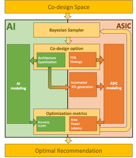
In our co-design method, we collate the Neural Network and ASIC design spaces and simultaneously optimize multiple objectives, using realistic metrics affected by a given set of choices. The Neural network design space consists of MLP architecture and heterogeneous quantization configuration. ASIC design space consists of the strategy used during ASIC synthesis. ASIC synthesis and Quantization Aware training within it gives a more accurate estimate of co-design objectives. Finally, an automated pipeline integrates all components to do multi-objective Bayesian optimization. This method keeps things simple, suitable, and sufficient for demonstrating our co-design approach.
3.1 Neural Network Architecture
We focus on Multi-Layer Perceptron (MLP) models consisting of fully connected layers. Despite their simplicity, they have been proven to be universal approximators, allowing them to approximate the most relevant functions with sufficient depth and width, both of which are included in the co-design space. While these parameters determine the model’s performance, they also determine the computational cost which scales as , where is the depth and is the width of each layer. Computational complexity affects relevant co-design objectives by influencing the area needed for memory and computation units, the power consumed for data storage and processing, and the latency required to compute each layer’s output.
3.2 Quantization Configuration
Quantization reduces the precision of the numerical representation of weights and activation functions from larger floating-point numbers to smaller fixed-point numbers, integers, or even binary numbers. Quantization can significantly decrease resource consumption for an MLP with a given width and depth without substantially affecting its performance. Heterogeneous quantization takes this idea further by aggressively quantizing less important layers to lower precision based on the importance of the layer to the overall performance in the network. So, we extend the co-design space of the neural network to include the layer-specific quantization configuration for MLP with given depth and widths.
3.3 ASIC Design
Recent years have witnessed a rapid growth in the availability of open-source process design kits (PDKs) and electronic design automation (EDA) tools for ASIC design. The first open-source PDK, for the SkyWater 130 nm CMOS process, was launched in 2020 in collaboration with Google. It has since been widely used for a variety of ASIC designs [12], including processors [41], coarse-grained reconfigurable arrays (CGRAs) [8] and AI accelerators [30, 31].
The standard open-source digital ASIC design flow for the SkyWater 130 nm process is OpenLANE, which is based on the OpenROAD project [2] and was first introduced by Shalan and Edwards in 2020 [36]. OpenLANE has been benchmarked against commercial EDA tools [41] and found to be comparable on key metrics such as synthesis run time, gate count, placement & routing time, die area, leakage power, placement density, and maximum clock frequency. However, its performance is typically to worse for most of these metrics. On the plus side, OpenLANE is highly automated, thus making it suitable for incorporation within Bayesian design space exploration.
3.4 Multi-objective Bayesian Optimization
The most limiting aspects of co-designing AI and ASIC are the high computational cost, exponential growth in design choices, and coupled competing objectives. The computing cost is even exacerbated when we include ASIC synthesis to get more accurate estimates of the ASIC objective metrics. Naively exploring the exponential and costly design space, like grid search, is inefficient, if not infeasible. To handle these challenges, we use Bayesian optimization, designed to minimize the number of expensive trials and proven to work effectively in domains including machine learning hyper-parameter tuning, algorithm selection, and control systems optimization. Being a black-box optimization, it also makes it easy to integrate and extend for further research. Additionally, it can be extended to globally optimize for multiple conflicting objectives, like accuracy and efficiency, in our co-design problem. The result of this optimization process gives us Pareto-optimal solutions that balance accuracy/efficiency trade-offs, enabling us to choose from a set of optimal designs of AI and ASIC.
3.5 Integration and Automation
While plenty of tools are available for NN modeling and some for ASIC synthesis, there is a high barrier between tools from both co-design domains. Our work bridges this much-needed gap through the seamless integration of these tools. Additionally, automation for going back and forth between NN training and ASIC synthesis is also lacking despite being crucial for co-design. Our work contributes to this by fully automating co-design optimization using the integrated tools. To make our tools accessible for future research, we exclusively use open-source tools.
4 Implementation
Our goal is to provide the research community with automated, open-source, extensible, and scalable tool integration that is familiar to researchers in both AI and ASIC domains. With this in mind, our automated pipeline uses Optuna for Bayesian optimization, QKeras for quantization-aware training, OpenLANE for ASIC synthesis, Hydra for easy configuration management, and Docker for containerization.
Optuna is a popular hyperparameter optimization library that offers features like parallelization and multiple optimization algorithms and is already popular among ML researchers. QKeras provides quantization-aware training for heterogeneously quantized models and is among the first few open-source libraries to do so. OpenLANE is an open-source ASIC synthesis tool that provides a complete RTL-to-GDSII flow. Hydra is implemented to allow easy switching between different Bayesian optimization algorithms, specifying co-design space and optimization objectives. Dockerization of both QKeras and OpenLANE enables easy scalability through the distributed parallelization that is well-integrated into Optuna.
The process proceeds as follows: Optuna suggests the MLP architecture, quantization configuration, and ASIC synthesis strategy for the subsequent trials based on the results of all previous choices and their effects on all optimization objectives. Each suggested trial is then handled by an ’orchestrator’ module that runs two containerized ’explorer modules’: (a) the NN Training module, which performs quantization-aware training using QKeras, following the suggested MLP architecture and quantization configuration and returns the validation loss of training; and (b) the ASIC Synthesis module, which automatically generates the RTL code for the suggested MLP architecture and quantization configuration using an easy-to-extend abstract syntax tree abstraction, and then runs the ASIC synthesis using OpenLANE to report on ASIC objectives like area, power, and delay by parsing the synthesis reports.
5 Experiment
As an example of practical importance, here we consider the problem of on-chip waveform processing for radiation detectors. The basic goal of waveform processing is real-time feature extraction from pulse shapes. The latter are generated by analog front-end (AFE) circuits that amplify and filter the charge packets generated by energetic particles [33]. A generic pulse can be written in the form
| (2) |
where is a reference pulse shape, is a scaling factor known as the pulse amplitude, is the time of arrival (TOA), and is additive noise. Note that is typically proportional to particle energy, so quantifying its value is a key goal of many measurements (which are known as amplitude spectroscopy). In other words, is the most important feature to be extracted from the waveform shape, . The TOA is also important in many cases since it encodes information on time of flight or arrival angle. Similarly, the reference shape can provide additional information, such as particle identification (PID) or the angle of arrival.
For simplicity, we assume that the feature extraction is performed digitally. In this case, the AFE is followed by an analog-to-digital converter (ADC) that converts to the discrete-time sequence
| (3) |
where denotes the sample index. The digitized reference shape, , depends on the particle type, detector material, and AFE filtering parameters. A commonly used model for is the so-called CR-(RC)N pulse shape, which is given by
| (4) |
where is the sampling period, is known as the order of the shaping function, and is the decay time constant.
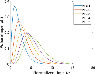
Fig. 2 plots in continuous time for various values of . Note that the waveform becomes smoother and more symmetric as increases due to the increased amount of low-pass filtering. The peak value of , which occurs at , is given by
| (5) |
The value of decreases monotonically with : from for to for . Also, the time at which the peak response occurs, (also known as the peaking time), is proportional to .
The quality of the received signal is quantified by the peak signal-to-noise ratio (PSNR), which is defined as
| (6) |
where is the standard deviation of the additive noise.
5.1 Dataset and Models

A set of noisy simulated pulses with the CR-(RC)n shape shown in Eqn. (4) was used for training. The noise component was assumed to be additive, white, and Gaussian (AWG). The peak amplitude varied randomly between pulses with a uniform distribution, resulting in a realistic PSNR range of 1 to 20 (0 dB to 26 dB). Pulse arrival times were randomly distributed following a Poisson distribution, as commonly encountered in experiments. Datasets with different values of (varying between 1-5) were used to study the impact of pulse shape changes.
Initial experiments were focused on datasets where both the pulse shape, , and the time constant, , were kept fixed. The feature extraction process then reduces to the single-variable problem of estimating the pulse amplitude, . An optimal solution to this problem exists when the noise is AWG in nature; it takes the form of a classical matched filter followed by peak picking [24]. However, note that this solution does not account for the inevitable overlap between nearby pulses, which is known as pileup.
Later simulations also allowed the time constant, , to vary randomly over the range , where is a constant. In this case, the feature extraction algorithm is asked to estimate both and , i.e., has to solve a two-variable problem.
The sampling rate for the simulations was initially set to . All processing was performed on data windows with data points. Variations in pulse arrival times within these windows, which are inevitable due to the asynchronous pulse arrivals, was minimized by a real-time waveform alignment algorithm. This algorithm operates as follows:
-
•
Buffer incoming data into windows of length .
-
•
Find the location within the buffer, , with the peak absolute value, .
-
•
Output the sub-window of length centered around the peak position, .
-
•
Buffer the next set of points and repeat.
Note that this algorithm makes no attempt to mitigate the effects of noise and pileup on . Thus, it only performs coarse time alignment of the received pulse waveforms.
Finally, the size of the neural network used for feature extraction was minimized by decimating the time-aligned waveforms, i.e., by increasing the sampling period from to where is an integer. This process reduces the length of each data window from to .
Our experiments used a default decimation factor of during the pre-processing stage, which results in windows containing 9 time points. Note that decimation also makes the estimation problem more challenging. The dataset was then split into training, validation, and test sets with a distribution of 70%, 20%, and 10%, respectively. This resulted in 69,008 samples for training, 19,716 for validation, and 9,859 for testing, ensuring comprehensive coverage across different phases of model evaluation
5.2 Co-design Space
The co-design choices for the experiment includes: a) the number of hidden layers, b) the number of perceptrons in each hidden layer, c) quantization levels of weights/biases between layers, d) input/output quantization levels for the MLP, and e) ASIC synthesis strategies. This makes the dimension of the co-design space to be:
| (7) |
where , , , , and are the number of choices available for input/output quantization, ASIC synthesis strategies, perceptrons in a layer, quantization levels in a layer, and the number of hidden layers, respectively. The range of values used in the experiment and consequently the dimension of the co-design space is shown in Table 1.
| Co-design Choices | Range |
|---|---|
| Hidden Layers | 1-3 |
| Perceptrons in a layer | 2-18 |
| Weights/Biases Quantizations | 2-16 |
| Input/Output Quantizations | 2-16 |
| ASIC Synthesis Strategies | 9 choices |
| Dimension of co-design space: 2,247,298,425 | |
6 Results
In this experiment, we defined co-design objectives, including the validation loss, area, power, and delay estimates reported from the ASIC synthesis. Some objectives, such as loss, area, and delay, are competitive, whereas others, like area and power, mostly overlap. There is no optimal solution in multi-objective optimization scenarios like this. Instead, a set of solutions exists where each is Pareto optimal—improvement in one objective necessitates a trade-off in another.
6.1 Pareto Fronts
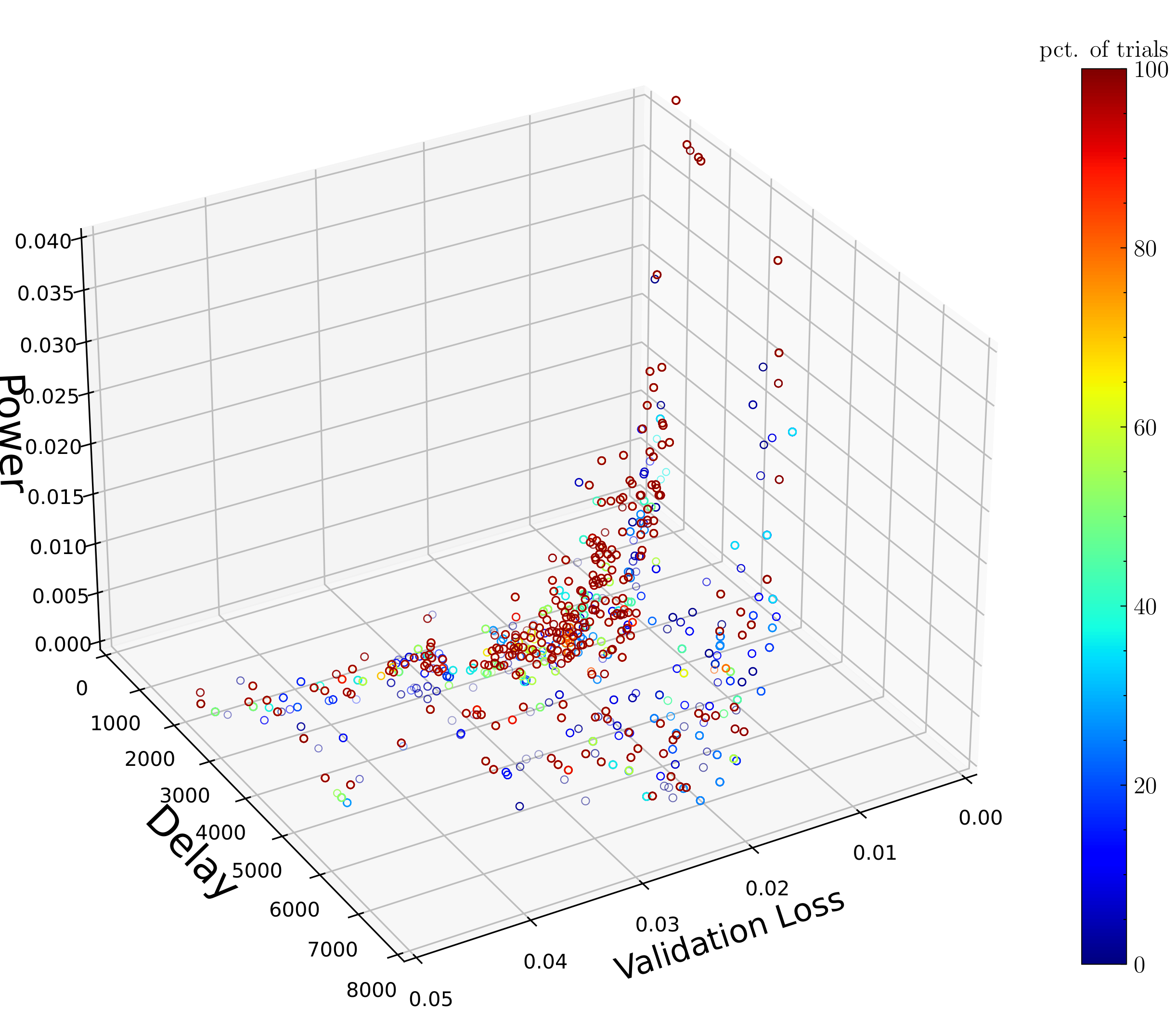
The 3D cross-section inf Fig. 4 reveals some insight into the search space explored during iterations. Early iterations, represented by blue points, are dispersed widely across the graph, indicating an initial exploration phase of the solution space. As the iterations advance, marked by a shift toward red points, there is a noticeable clustering of data points, suggesting that the optimization algorithm is converging toward a set of optimal solutions and also reveals the topology of the front (we will continue this discussion in a later section). Meanwhile, the topology of the Pareto-front is also shown in those clusters, which brings us to the next set of figures on 2D cross-sections (Figs. 5 - 7), which gives more insight into the topology of the front.
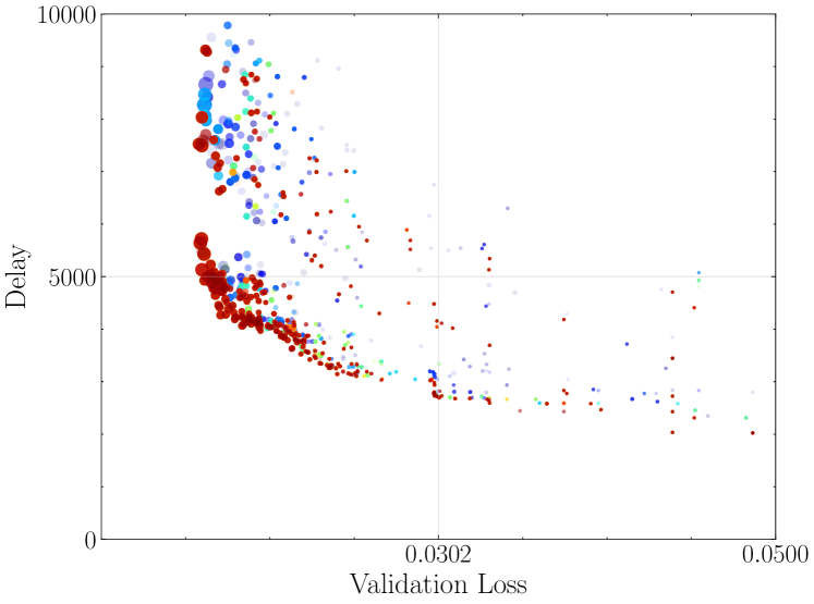
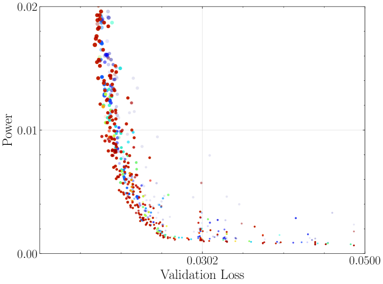
The 2D cross-section plots The most clear boundary appears when loss and power are trying to be balanced. Fig. 7 reveals a steep relationship between validation loss and power, indicating significant challenges in achieving lower validation losses. Points even from early iterations densely cluster at lower validation loss levels, suggesting the algorithm quickly reaches this boundary where further reductions in loss require disproportionately higher power consumption. Moreover, the dense clustering of data points along the curve suggests a robust and predictable trade-off between these objectives. The topology of this Pareto front is smoother and more continuous compared to the other cross-sections, indicating that the optimization paths for reducing validation loss are closely tied to increases in power usage. The narrow variance is likely the reason behind previous success of loss-power optimization based on theoretical estimates implemented in popular libraries seems to do well enough.
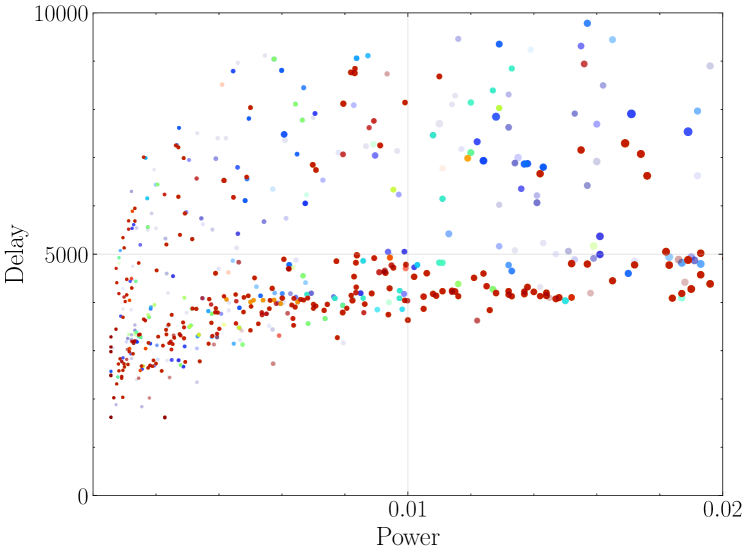
The delay-power boundary can be seen in Fig. 6, which reveals a broad spread of data points, indicating a diverse range of outcomes. Lower power can sometimes be achieved with high and low delays, further complicating the trade-offs. This distribution suggests that finding configurations that optimize one or both metrics might be possible without a direct correlation between increased power and increased delay.
The Fig. 7 also explores the relationship between delay and validation loss. Like Fig. 5, there is a visible concentration of points towards lower validation losses with varying degrees of delay. Notably, the delay does not show a clear upward or downward trend with decreasing validation loss, suggesting a more complex relationship where specific configurations might optimize delay without significantly impacting validation loss. Complex dynamics like this are one of the justifications of our approach, in that some of the ASIC synthesis metrics are hard to estimate using a theoretical approach.
6.2 Optimization Dynamics
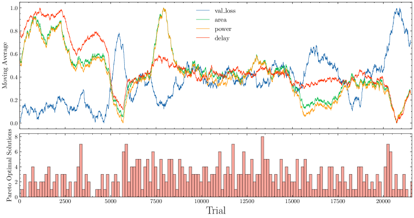
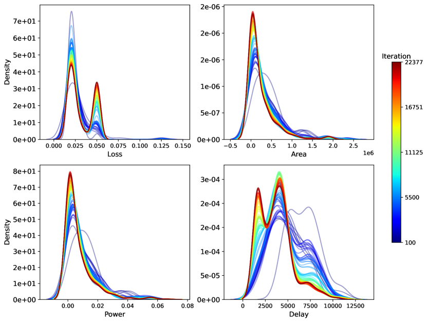
Fig. 8 shows the moving average of the optimization objectives as the search progresses. The histogram shows the number of Pareto optimal solutions during that evolution. The histogram shows that increasing iterations consistently find Pareto optimal points throughout the optimization. The Fig. 9 shows the kernel density estimate (KDE) of objectives in Pareto fronts during different iterations.
There are several key observations from the optimization dynamics that can be gained from Fig. 8 and Fig. 9. First, the search increasingly goes from the region where loss is low to higher, apparent in both Fig. 8 and the top-left of Fig. 9. The second peak on the validation loss that is not being pushed further is also close to the baseline validation from a model that always predicts the average of the training set. This is happening because no constraint minimal performance was set during this round of simulation. There is a high sensitivity of area/power with the validation loss, whereas delay is less susceptible to it, both of which were also hinted previously by Figs. 5-7. Kernel density estimates from Fig. 9 indicate a successful focusing of the search towards promising regions, with area/power being most challenging for the optimization to push lower. The dynamics of delay seen in both Fig. 8 and Fig 9 clearly show that it benefited the most from the higher iteration of optimization.
6.3 Convergence
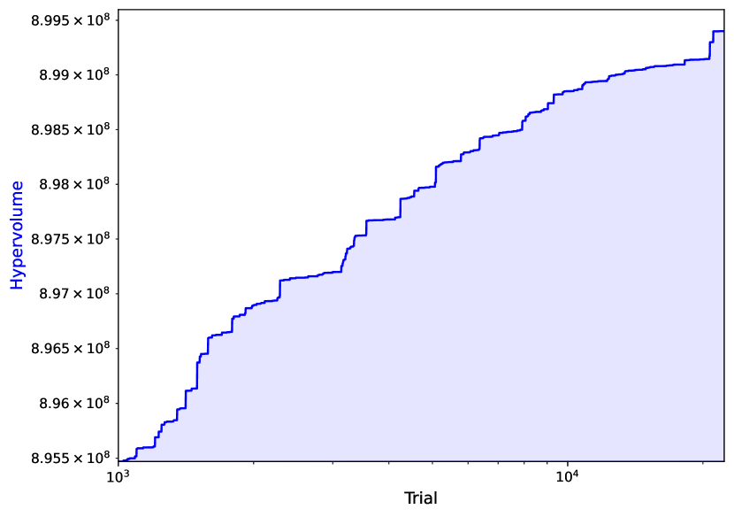
Hypervolume is one of the key metrics used to evaluate the dynamics of the Multi-Objective Bayesian Optimization (MOBO). The hypervolume measures the extent of the objective space covered by the Pareto front, bounded by a reference point, which, in this context, is the worst-case scenario for each objective. A larger hypervolume indicates superior solution quality, encompassing more objective space. This metric is also helpful as a convergence test during the optimization process.The hypervolume increases and eventually saturates in our experiments, as illustrated in the Figure 10. This saturation suggests that the optimization process in our experiment has effectively converged to a stable set of optimal solutions.
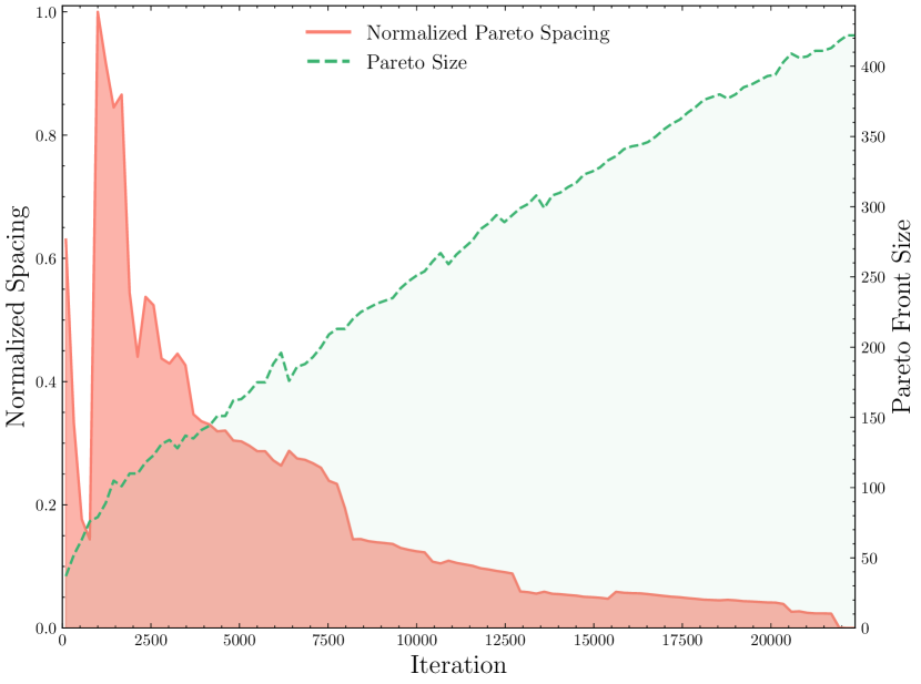
Pareto Diversity and Spacing: Additionally, we use Pareto diversity and spacing to characterize the effectiveness of our method. Pareto diversity ensures that the optimization covers a broad range of trade-offs, enhancing decision-making with diverse solutions. Meanwhile, spacing between these points measures how uniformly solutions are distributed, indicating a balanced solution space exploration. In Fig. 11, we observe the evolution of these metrics in our experiment. The normalized Pareto spacing decreases, showing an increase in uniformity among solutions. Meanwhile, the Pareto size increases, indicating many optimal solutions. This shows that the algorithm efficiently populates the objective space with well-distributed, diverse solutions.
6.4 Optimal Designs
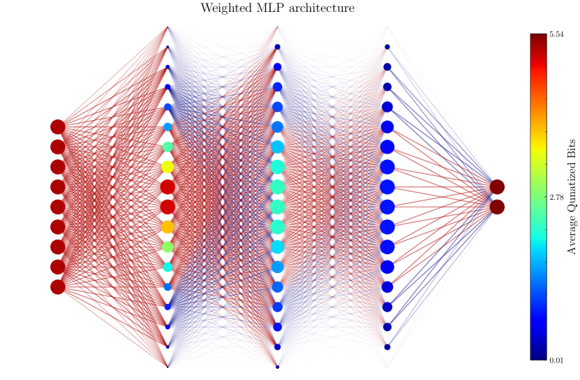
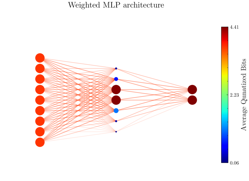
The visual representation in Fig. 12 represents an average Multi-Layer Perceptron (MLP) architecture derived from a set of Pareto optimal solutions from optimization in a co-design space with over two billion possible configurations. This MLP model embodies the collective characteristics from various configurations, differing depth, width, and quantization levels for each layer. The size and color of the perceptron represent the average quantization done in that perceptron in all optimal solutions with nodes that are absent in a configuration represented with zero. The input-output quantization is represented in the final layer of the MLP. Fig. 12 hints that the most detrimental effect of co-design is lower quantization in input and output data.
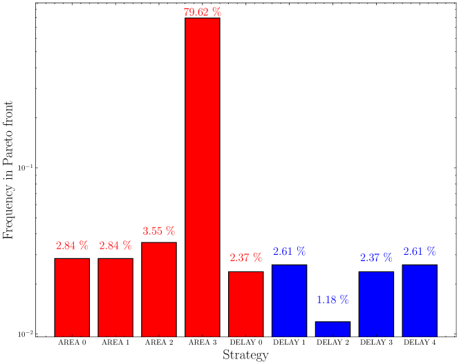
Fig. 13 presents the distribution of various synthesis strategies at the Pareto front, effectively illustrating the predominance of specific strategies over others in achieving optimal design configurations.
Notably, the ‘AREA 3’ strategy dominates the distribution, representing a staggering 79.62% of the choices at the Pareto front, indicating its effectiveness in optimizing the design parameters within the constraints provided. This could simply be because the optimization objective includes both area and power, and AREA 3 is the most aggressive optimization for the area and, hence, for power, too. A new simulation run with weighted values for area and power can be used to confirm this hypothesis.
The other area strategies, each account for a relatively minor portion of the Pareto front, all below 4%, suggesting that while these strategies contribute to the Pareto front, they are significantly less effective compared to ”AREA 3”. The significantly small role of DELAY 2 remains to be understood.
6.5 Comparison with Theory
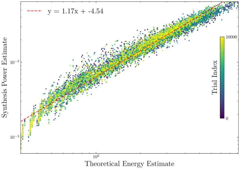
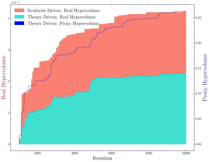
In this section, we do another experiment to quantify the distinction in our approach, where we used a power estimate from ASIC synthesis instead of the theoretical estimate. Fig. 14(a) shows that the theoretical estimate of the energy shows a strong correlation with the power estimated from the ASIC synthesis. Still, the uncertainty of its accuracy can affect the search significantly. To quantify the effect of unquantified uncertainty in the theoretical estimate, we ran another round of two-objective optimization:a a) Area-Energy optimization guided by a theoretical estimate of energy given by QKeras, and b) Power-energy optimization guided by power estimated from logic synthesis.
To compare the effectiveness of the two approaches, Fig. 14(b) shows the hypervolume evolution during the two optimization runs, with a red-dashed line showing the proxy-hypervolume used in theory-guided optimization. While the red curve shows an increase and saturation like the synthesis-guided hypervolume, the plotting of ‘real hypervolume’ computed using power estimate from synthesis clearly shows that theory-driven optimization saturates much earlier with very little Pareto diversity. This empirical observation is the first insight into the negative impact of theory-driven optimization for realistic ASIC design solutions, with more in our future works.
6.6 In-Pixel Implementable Neural Network
We applied constraints on the trials to identify those suitable for in-pixel implementation, as shown in Table 2. We chose the area constraint of 250 x 250 m2 based on the 130nm process design kit (PDK) used. The acceptable power density limit of 5 W/cm2 was set to ensure feasible on-chip power consumption. The delay constraint of 20 ps was derived from the clock frequency used in our design. The validation Mean Squared Error (MSE) threshold of 0.044837 corresponds to the MSE of a simple baseline model that predicts the mean of the training data. These constraints collectively define a challenging yet realistic design space for in-pixel neural network implementation, pushing our co-design approach to find optimal solutions that balance performance with hardware limitations.
| Parameter | Maximum Constraint |
|---|---|
| Area | 250 x 250 |
| Power Density | 5 W/cm2 |
| Delay | 20 ps |
| Val. MSE | 0.044837 |
Applying the constraints to the trials reveals a Pareto front with 54 in-pixel implementable, equally good choices. Figure 15 plots the optimization objectives in the constrained Pareto surface. The x-axis represents the area utilization, which is the fraction of area occupied compared to the constraint set. The y-axis shows the power density in W/cm². The z-axis and color scale represent , a performance metric of the model defined as the ratio of the baseline MSE to the model’s MSE (MSE of the baseline / MSE of the model). The top plot illustrates the relationship between area utilization, power density, and . The surface shows a complex landscape with multiple peaks and valleys, indicating the trade-offs between these parameters. Generally, we can observe that higher values (better performance) tend to correspond with higher power density and area utilization, as expected for more complex models. The bottom plot focuses on , which represents the maximum achievable frequency for each design point. This plot reveals a different pattern of trade-offs, with peaks in occurring at various combinations of area utilization and power density.
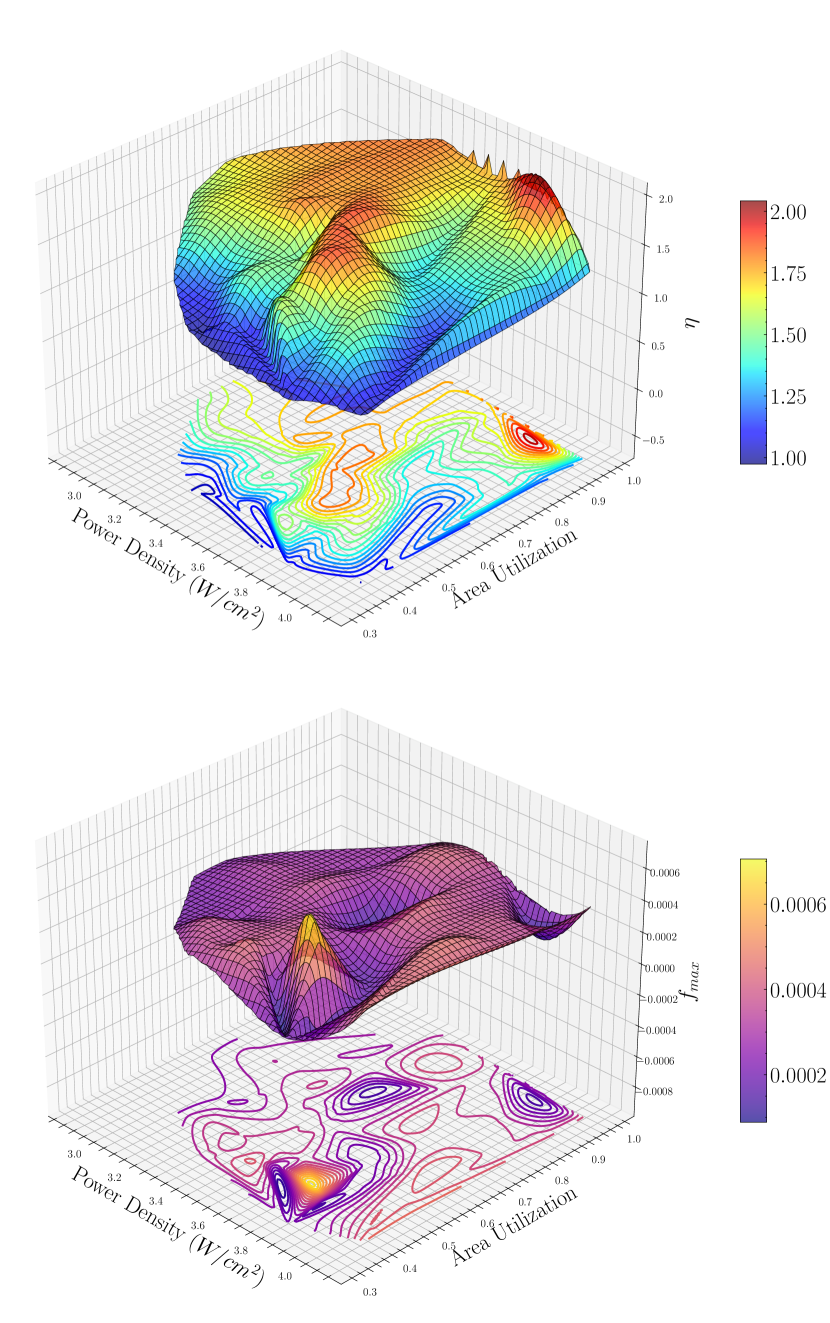
To further evaluate the effectiveness of using theoretical estimates for guidance versus our approach using ASIC synthesis, we identified the constrained Pareto fronts in the two-objective (performance and power) optimization done in 6.5. The figure 15 clearly demonstrates that utilizing synthesis-guided metrics in the optimization process revealed a constrained Pareto front with a greater number of in-pixel implementable design choices, each exhibiting better area and power efficiency compared to those obtained using theoretical estimate.
7 Conclusion and Future Work
In this paper, we presented a holistic approach to co-designing neural networks and ASICs for enabling in-pixel intelligence in radiation detectors. Our key contributions include an automated pipeline integrating neural network design and ASIC synthesis within a multi-objective Bayesian optimization framework, use of realistic ASIC synthesis metrics rather than theoretical estimates to guide the optimization process for practical solutions, and exploration of a specific large co-design space including neural architecture, quantization, and ASIC synthesis strategies. We demonstrated Pareto-optimal designs meeting strict area, power, and latency constraints for in-pixel implementation.
Our results show the benefits of using circuit-level metrics from ASIC synthesis compared to theoretical estimates, which can lead to less ideal solutions even in cases when such approximations are available. This approach provides more accurate guidance towards implementable designs.
There are several promising directions for future work. Expanding the co-design space to include additional neural architectures beyond MLPs could yield more powerful in-pixel processing capabilities. Incorporating more detailed circuit-level optimization choices into the co-design process may uncover additional efficiency gains. Exploring more emerging technologies could push the boundaries of what’s possible with in-pixel processing. Finally, extending this approach to other scientific applications requiring extreme edge AI could have broad impact across various fields.
8 Acknowledgement
This manuscript has been authored by Brookhaven Science Associates, LLC under Contract No. DE-SC0012704 with the U.S. Department of Energy. The United States Government retains and the publisher, by accepting the article for publication, acknowledges that the United States Government retains a non-exclusive, paid-up, irrevocable, world-wide license to publish or reproduce the published form of this manuscript, or allow others to do so, for United States Government purposes. This work was supported by the Laboratory Directed Research and Development (LDRD) Program of Brookhaven National Laboratory under U.S. Department of Energy Contract No. DE-SC0012704. The authors would also like to thank Dr. Sandeep Miryala and Dr. Sanket Jantre for numerous helpful discussions.
References
- [1] Abdelfattah, M. S., Dudziak, Ł., Chau, T., Lee, R., Kim, H., and Lane, N. D. Best of both worlds: AutoML codesign of a CNN and its hardware accelerator. In 2020 57th ACM/IEEE Design Automation Conference (DAC) (2020), IEEE, pp. 1–6.
- [2] Ajayi, T., Chhabria, V. A., Fogaça, M., Hashemi, S., Hosny, A., Kahng, A. B., Kim, M., Lee, J., Mallappa, U., Neseem, M., et al. Toward an open-source digital flow: First learnings from the OpenROAD project. In Proceedings of the 56th Annual Design Automation Conference 2019 (2019), pp. 1–4.
- [3] Albertsson, K., Altoe, P., Anderson, D., Andrews, M., Espinosa, J. P. A., Aurisano, A., Basara, L., Bevan, A., Bhimji, W., Bonacorsi, D., et al. Machine learning in high energy physics community white paper. In Journal of Physics: Conference Series (sep 2018), vol. 1085, IOP Publishing, p. 022008.
- [4] Bourilkov, D. Machine and deep learning applications in particle physics. International Journal of Modern Physics A 34, 35 (2019), 1930019.
- [5] Bringmann, O., Ecker, W., Feldner, I., Frischknecht, A., Gerum, C., Hämäläinen, T., Hanif, M. A., Klaiber, M. J., Mueller-Gritschneder, D., Bernardo, P. P., et al. Automated HW/SW co-design for edge AI: State, challenges and steps ahead. In Proceedings of the 2021 International Conference on Hardware/Software Codesign and System Synthesis (2021), pp. 11–20.
- [6] Brooks, D. M., Bose, P., Schuster, S. E., Jacobson, H., Kudva, P. N., Buyuktosunoglu, A., Wellman, J., Zyuban, V., Gupta, M., and Cook, P. W. Power-aware microarchitecture: Design and modeling challenges for next-generation microprocessors. IEEE Micro 20, 6 (2000), 26–44.
- [7] Campos, J., Dong, Z., Duarte, J., Gholami, A., Mahoney, M. W., Mitrevski, J., and Tran, N. End-to-end codesign of Hessian-aware quantized neural networks for FPGAs and ASICs. arXiv preprint arXiv:2304.06745 (2023).
- [8] Chen, P.-H., Tsao, C., and Raina, P. An open-source coarse-grained reconfigurable array using SkyWater 130 nm technology and agile hardware design flow. In 2023 IEEE International Symposium on Circuits and Systems (ISCAS) (2023), IEEE, pp. 1–5.
- [9] Coelho, C. N., Kuusela, A., Li, S., Zhuang, H., Ngadiuba, J., Aarrestad, T. K., Loncar, V., Pierini, M., Pol, A. A., and Summers, S. Automatic heterogeneous quantization of deep neural networks for low-latency inference on the edge for particle detectors. Nature Machine Intelligence 3, 8 (2021), 675–686.
- [10] Deiana, A. M., Tran, N., Agar, J., Blott, M., Di Guglielmo, G., Duarte, J., Harris, P., Hauck, S., Liu, M., Neubauer, M. S., et al. Applications and techniques for fast machine learning in science. Frontiers in Big Data 5 (2022), 787421.
- [11] Di Guglielmo, G., Fahim, F., Herwig, C., Valentin, M. B., Duarte, J., Gingu, C., Harris, P., Hirschauer, J., Kwok, M., Loncar, V., et al. A reconfigurable neural network ASIC for detector front-end data compression at the HL-LHC. IEEE Transactions on Nuclear Science 68, 8 (2021), 2179–2186.
- [12] Edwards, R. T., Shalan, M., and Kassem, M. Real silicon using open-source EDA. IEEE Design & Test 38, 2 (2021), 38–44.
- [13] Gao, C., Rios-Navarro, A., Chen, X., Liu, S.-C., and Delbruck, T. EdgeDRNN: Recurrent neural network accelerator for edge inference. IEEE Journal on Emerging and Selected Topics in Circuits and Systems 10, 4 (2020), 419–432.
- [14] Gorni, D., Carini, G., Deptuch, G., Kuczewski, A., Maj, P., Mandal, S., Pinaroli, G., Rumaiz, A., Siddons, D., and John, N. Integration of EDWARD readout architecture in full-field fluorescence imaging detector. Journal of Instrumentation 19, 04 (apr 2024), C04035.
- [15] Govorkova, E., Puljak, E., Aarrestad, T., James, T., Loncar, V., Pierini, M., Pol, A. A., Ghielmetti, N., Graczyk, M., Summers, S., et al. Autoencoders on field-programmable gate arrays for real-time, unsupervised new physics detection at 40 MHz at the Large Hadron Collider. Nature Machine Intelligence 4, 2 (2022), 154–161.
- [16] Groettvik, O., collaboration, A., et al. ALICE ITS3: A bent stitched MAPS-based vertex detector. Journal of Instrumentation 19, 02 (2024), C02048.
- [17] Hawks, B., Duarte, J., Fraser, N. J., Pappalardo, A., Tran, N., and Umuroglu, Y. Ps and Qs: Quantization-aware pruning for efficient low latency neural network inference. Frontiers in Artificial Intelligence 4 (2021), 676564.
- [18] Horowitz, M. 1.1 Computing’s energy problem (and what we can do about it). In 2014 IEEE International Solid-State Circuits Conference (ISSCC) Digest of Technical Papers (2014), IEEE, pp. 10–14.
- [19] Horowitz, M., Indermaur, T., and Gonzalez, R. Low-power digital design. In Proceedings of 1994 IEEE symposium on low power electronics (1994), IEEE, pp. 8–11.
- [20] Houshmand, P., Sarda, G. M., Jain, V., Ueyoshi, K., Papistas, I. A., Shi, M., Zheng, Q., Bhattacharjee, D., Mallik, A., Debacker, P., et al. DIANA: An end-to-end hybrid digital and analog neural network SoC for the edge. IEEE Journal of Solid-State Circuits 58, 1 (2022), 203–215.
- [21] Jiang, W., Yang, L., Sha, E. H.-M., Zhuge, Q., Gu, S., Dasgupta, S., Shi, Y., and Hu, J. Hardware/software co-exploration of neural architectures. IEEE Transactions on Computer-Aided Design of Integrated Circuits and Systems 39, 12 (2020), 4805–4815.
- [22] Li, E., Zeng, L., Zhou, Z., and Chen, X. Edge AI: On-demand accelerating deep neural network inference via edge computing. IEEE Transactions on Wireless Communications 19, 1 (2019), 447–457.
- [23] Liang, T., Glossner, J., Wang, L., Shi, S., and Zhang, X. Pruning and quantization for deep neural network acceleration: A survey. Neurocomputing 461 (2021), 370–403.
- [24] Mandal, S., Deptuch, G., and Carini, G. Real-time feature extraction for readout ASICs: Algorithms and on-chip implementations. In 2023 IEEE Nuclear Science Symposium, Medical Imaging Conference and International Symposium on Room-Temperature Semiconductor Detectors (NSS MIC RTSD) (2023), IEEE, pp. 1–1.
- [25] Mazumder, A. N., Meng, J., Rashid, H.-A., Kallakuri, U., Zhang, X., Seo, J.-S., and Mohsenin, T. A survey on the optimization of neural network accelerators for micro-AI on-device inference. IEEE Journal on Emerging and Selected Topics in Circuits and Systems 11, 4 (2021), 532–547.
- [26] Merenda, M., Porcaro, C., and Iero, D. Edge machine learning for AI-enabled IoT devices: A review. Sensors 20, 9 (2020), 2533.
- [27] Miryala, S., Carini, G., Deptuch, G., Huang, J., Katkoori, S., Maj, P., Mandal, S., Ren, Y., and Zaman, M. A. Design and challenges of edge computing ASICs on front-end electronics. In 2022 23rd International Symposium on Quality Electronic Design (ISQED) (2022), IEEE, pp. 19–27.
- [28] Miryala, S., Mittal, S., Ren, Y., Carini, G., Deptuch, G., Fried, J., Yoo, S., and Zohar, S. Waveform processing using neural network algorithms on the front-end electronics. Journal of Instrumentation 17, 01 (2022), C01039.
- [29] Miryala, S., Zaman, M. A., Mittal, S., Ren, Y., Deptuch, G., Carini, G., Zohar, S., Yoo, S., Fried, J., Huang, J., et al. Peak prediction using multi layer perceptron (MLP) for edge computing ASICs targeting scientific applications. In 2022 23rd International Symposium on Quality Electronic Design (ISQED) (2022), IEEE, pp. 1–6.
- [30] Modaresi, F., Guthaus, M., and Eshraghian, J. K. OpenSpike: An OpenRAM SNN accelerator. In 2023 IEEE International Symposium on Circuits and Systems (ISCAS) (2023), IEEE, pp. 1–5.
- [31] Parmar, V., Ray, A., Moorthii, C., Mishra, R., Verma, D., Pandey, D., and Suri, M. Open-RIMC: Open-source RRAM-based IMC co-processor with reconfigurable logic mapping. In 2023 IEEE 23rd International Conference on Nanotechnology (NANO) (2023), IEEE, pp. 519–523.
- [32] Prabhu, K., Gural, A., Khan, Z. F., Radway, R. M., Giordano, M., Koul, K., Doshi, R., Kustin, J. W., Liu, T., Lopes, G. B., et al. CHIMERA: A 0.92-TOPS, 2.2-TOPS/W edge AI accelerator with 2-MByte on-chip foundry resistive RAM for efficient training and inference. IEEE Journal of Solid-State Circuits 57, 4 (2022), 1013–1026.
- [33] Radeka, V. Signal processing for particle detectors: Particle detectors and detector systems. Detectors for Particles and Radiation. Part 1: Principles and Methods (2011), 288–319.
- [34] Reagen, B., Hernández-Lobato, J. M., Adolf, R., Gelbart, M., Whatmough, P., Wei, G.-Y., and Brooks, D. A case for efficient accelerator design space exploration via Bayesian optimization. In 2017 IEEE/ACM International Symposium on Low Power Electronics and Design (ISLPED) (2017), IEEE, pp. 1–6.
- [35] Rinella, G. A., Andronic, A., Antonelli, M., Aresti, M., Baccomi, R., Becht, P., Beole, S., Braach, J., Buckland, M. D., Buschmann, E., et al. Digital pixel test structures implemented in a 65 nm CMOS process. Nuclear Instruments and Methods in Physics Research Section A: Accelerators, Spectrometers, Detectors and Associated Equipment 1056 (2023), 168589.
- [36] Shalan, M., and Edwards, T. Building OpenLANE: A 130nm OpenROAD-based tapeout-proven flow. In Proceedings of the 39th International Conference on Computer-Aided Design (2020), pp. 1–6.
- [37] Shi, Z., Sakhuja, C., Hashemi, M., Swersky, K., and Lin, C. Using Bayesian optimization for hardware/software co-design of neural accelerators. In Workshop on ML for Systems at the Conference on Neural Information Processing Systems (NeurIPS) (2020).
- [38] Sipola, T., Alatalo, J., Kokkonen, T., and Rantonen, M. Artificial intelligence in the IoT era: A review of edge AI hardware and software. In 2022 31st Conference of Open Innovations Association (FRUCT) (2022), IEEE, pp. 320–331.
- [39] Wang, X., Han, Y., Leung, V. C., Niyato, D., Yan, X., and Chen, X. Edge AI: Convergence of edge computing and artificial intelligence. Springer, 2020.
- [40] Zhang, X., Li, Y., Pan, J., and Chen, D. Algorithm/accelerator co-design and co-search for edge AI. IEEE Transactions on Circuits and Systems II: Express Briefs 69, 7 (2022), 3064–3070.
- [41] Zhu, Y., Yin, G., Wang, X., Yang, Q., Luan, Z., Zhang, Y., Wang, M., Guo, P., Wan, X., Hu, S., et al. GreenRio: A modern RISC-V microprocessor completely designed with a open-source EDA flow. In Proceedings of the Workshop on Open-Source EDA Technology (WOSET) (2022).