Experimental Demonstration of Efficient and Polarization-Diversity Fiber-Chip Coupling by 2D Grating Couplers with 193-nm DUV Lithography
Two-dimensional (2D) diffractive gratings offer a polarization-independent coupling solution between optical fibers and photonic integrated circuits, with advantages including placement flexibility, ease of fabrication, and tolerance to alignment errors. In this work, we proposed and experimentally demonstrated a highly efficient 2D grating coupler fabricated with 193-nm deep-ultraviolet (DUV) lithography on the 220-nm silicon-on-insulator (SOI) platform. An experimental peak coupling efficiency of -2.54 dB can be obtained using a minimum feature size of 180 nm, relying on the novel double-layer 2D grating structure. The proposed 2D waveguide grating is composed of a 70-nm shallow-etched hole array and a 160-nm-thick deposited polycrystalline silicon tooth array. The demonstrated design exhibits a 3-dB bandwidth of 23.4 nm with good positioning tolerance for optical fibers. Due to the benefits of perfectly vertical coupling configuration, the measured polarization-dependent loss in experiments is below 0.3 dB within the 3-dB working bandwidth. Our proposed double-layer 2D gratings can also be applied to other integrated optics platforms, where the grating directionality can be enhanced by optimizing the front-end-of-line process to break the vertical symmetry, thus enabling an efficient and polarization-independent coupling between optical fibers and photonic chips.
Introduction
Silicon photonics platform has experienced significant growth over the last decade, with high-bandwidth optical transceivers for telecom and datacom now being mass-produced and transitioning into on-board and in-package optical interconnects [1, 2, 3]. Various emerging applications, such as programmable photonic processors [4, 5, 6] and prototypes for optical sensing and imaging [7, 8] have been successfully demonstrated. The appeal of silicon photonics lies in its ability to leverage the well-established complementary metal-oxide-semiconductor (CMOS) compatible fabrication processes. Additionally, the high refractive index contrast enables the strong confinement of optical field, resulting in the reduction of the form factor of optical components and circuits. However, this has also caused a significant challenge in achieving optimal fiber-chip coupling interfaces due to the huge difference in mode size between optical fibers and silicon waveguides.
Both in-plane and out-of-plane coupling strategies have been extensively researched over the years [9, 10]. While edge couplers exhibit low polarization dependence and high coupling efficiency, they typically require high-quality facets on the chip sides. Out-of-plane coupling, utilizing diffractive gratings, has been widely adopted in wafer-scale testing due to its advantages of simple back-end processing, position flexibility and low alignment accuracy requirements [10, 11]. Nevertheless, the one-dimensional (1D) grating coupler typically manifests a strong polarization dependence and work optimally only for certain linear polarization state [12]. Subwavelength gratings can support both transverse electric (TE) and transverse magnetic (TM) modes, allowing for polarization-insensitive fiber-chip coupling [13, 14, 15]. However, additional polarization splitters and rotators are necessary to convert the TM mode into the TE mode, as most photonic integrated components for optical interconnects are designed for the TE mode [9]. Two-dimensional (2D) grating couplers provide an alternative solution for polarization-insensitive coupling [16]. They can be viewed as a superposition of two 1D grating couplers placed perpendicular to each other, thus can convert any arbitrary polarized light from the optical fiber into two orthogonal TE modes on a photonic chip. Given that 2D grating couplers are capable of achieving polarization splitting and rotation simultaneously, they can be effectively utilized in the polarization-diversity receivers [17, 18].
Nonetheless, the primary challenge with 2D grating couplers is achieving a high coupling efficiency while accommodating the 193 nm deep-ultraviolet (DUV) lithography that is currently provided by the majority of commercial silicon photonics foundries [19]. While it has been shown that coupling loss can be effectively reduced to around -2.5 dB per interface by either increasing the thickness of the crystalline silicon layer to 340 nm [20], or by employing blazed subwavelength structures with a minimum feature size of 40 nm [21], these approaches do not provide a direct solution for the prevalent 220-nm silicon-on-insulator (SOI) wafers that are based on the 130 nm or 180 nm CMOS node toolset [19]. To address this issue, one might intuitively replicate the double-layer structure strategy previously reported for efficient 1D grating couplers [22, 23, 24]. This involves depositing an additional layer of polycrystalline silicon (poly-Si) or silicon nitride () on top of the SOI to break vertical symmetry and enhance directionality, which is the ratio of upward diffracted optical energy to the total radiated optical power. The deposition of additional poly-Si or has become a de facto standard in commercial silicon photonic foundries, for example, to couple light from the silicon waveguide to the germanium waveguide by using a taper in poly-Si for photodetection [25]. However, it is difficult to realize an efficient 2D grating coupler assisted with the double-layer structure while also adhering to fabrication constraints, which has not yet been experimentally demonstrated before [26, 27].
In this work, we present the first experimental demonstration of a highly efficient 2D graing coupler fabricated on the 220-nm SOI platform with 193-nm DUV lithography for standard single-mode fibers (SMFs). The demonstrated fiber-to-chip coupling efficiency is -2.54 dB (56%) with a 3-dB bandwidth of 23.4 nm. Our measurements indicate a polarization-dependence loss (PDL) <0.3 dB, attributed to the perfect vertical coupling configuration. The proposed double-layer 2D grating includes 70 nm shallowly etched holes on the 220 nm thick SOI and 160 nm thick aligned poly-Si teeth deposited on top. The detailed deign, simulation results, and fabrication tolerances are presented in Section II, followed by the fabrication and experimental performance validation in Sections III.
Design and Simulation
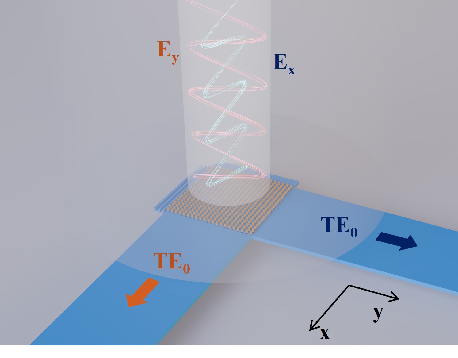
Fig. 1 illustrates the conceptual diagram of the 2D grating coupler bridged with a SMF in perfectly vertical coupling configuration. The two orthogonal polarizations, Ex and Ey in a SMF can be coupled and split into the fundamental TE mode of the two perpendicular silicon waveguides on a photonic chip. A low PDL can be maintained due to the adopted perfectly vertical coupling. In order to achieve a uniform coupling performance for both polarizations, the grating is designed to be symmetrical along its diagonal axis. The device is designed to be fabricated on a 220-nm-thick SOI platform with a buried-oxide thickness of 2 µm. The 70-nm shallow etch process is utilized to form the low refractive index region in the grating region. For grating couplers, the coupling efficiency (CE) performance is mainly determined by its directionality and the modal overlap condition. For example, bottom mirrors can also be deposited beneath the grating area to enhance the constructive interference diffracted upward [28]. To match the diffracted optical field with the mode field distribution in a SMF, the grating period or duty cycle can be apodized to adjust the grating strength [29]. In our proposed design, poly-Si layer is employed to improve the directionality of the grating. Fig. 2(a) illustrates a 2D grating design with double-layer structure, including a 220-nm-thick crystalline Si, an array of 70 nm circular etched holes, and 160 nm thick poly-Si teeth deposited on top. Break of the vertical structural symmetry can enhance the constructive interference upward, thus improving the directionality and CE of the grating coupler. However, due to the excessively strong grating strength, most of the optical power is diffracted within the first few grating periods, as illustrated in the top view and cross-sectional view of the optical field profile in the grating region in Fig. 2(a). Such large grating strength is mainly due to the high refractive index difference between the 380 nm thick Si and 150 nm thick Si. Hence, a significant field mismatch can be observed when compared with the Gaussian-like optical field distribution in an SMF, which is shown in Fig. 2(c). For 1D grating couplers, modal overlap condition can be mitigated by moving the center of the optical fiber to the front of the grating region. However, this is not feasible for a 2D grating as the optical fiber must be positioned at the grating center to minimize PDL for both polarization directions. Although grating period apodization can adjust the grating strength to a certain degree, this approach is very limited in our case. with possible issues such as violating the minimum feature size (MFS) for fabrication.
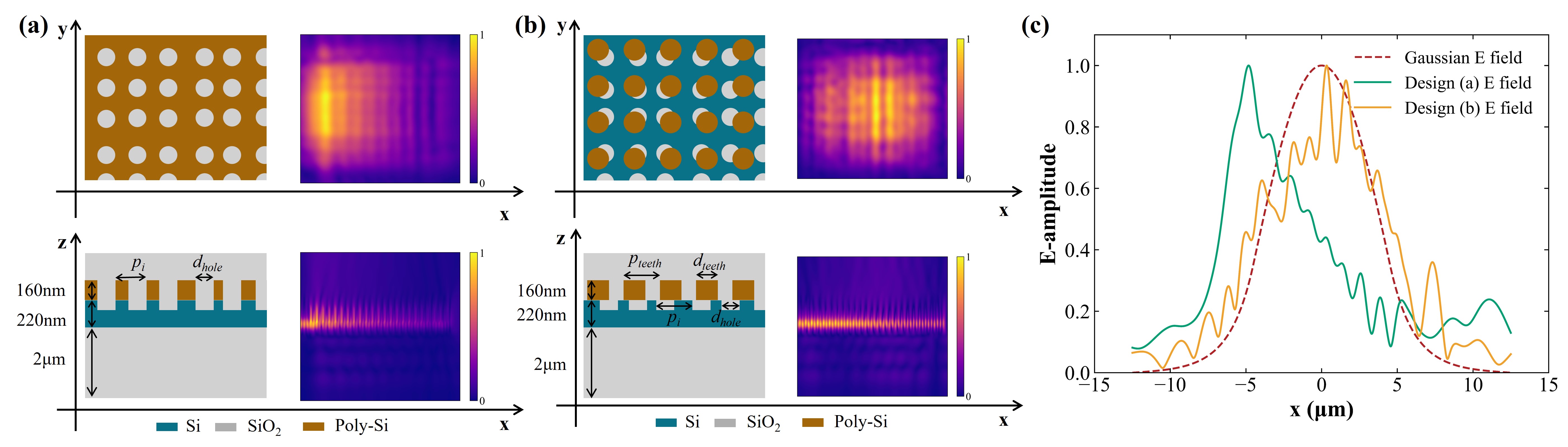
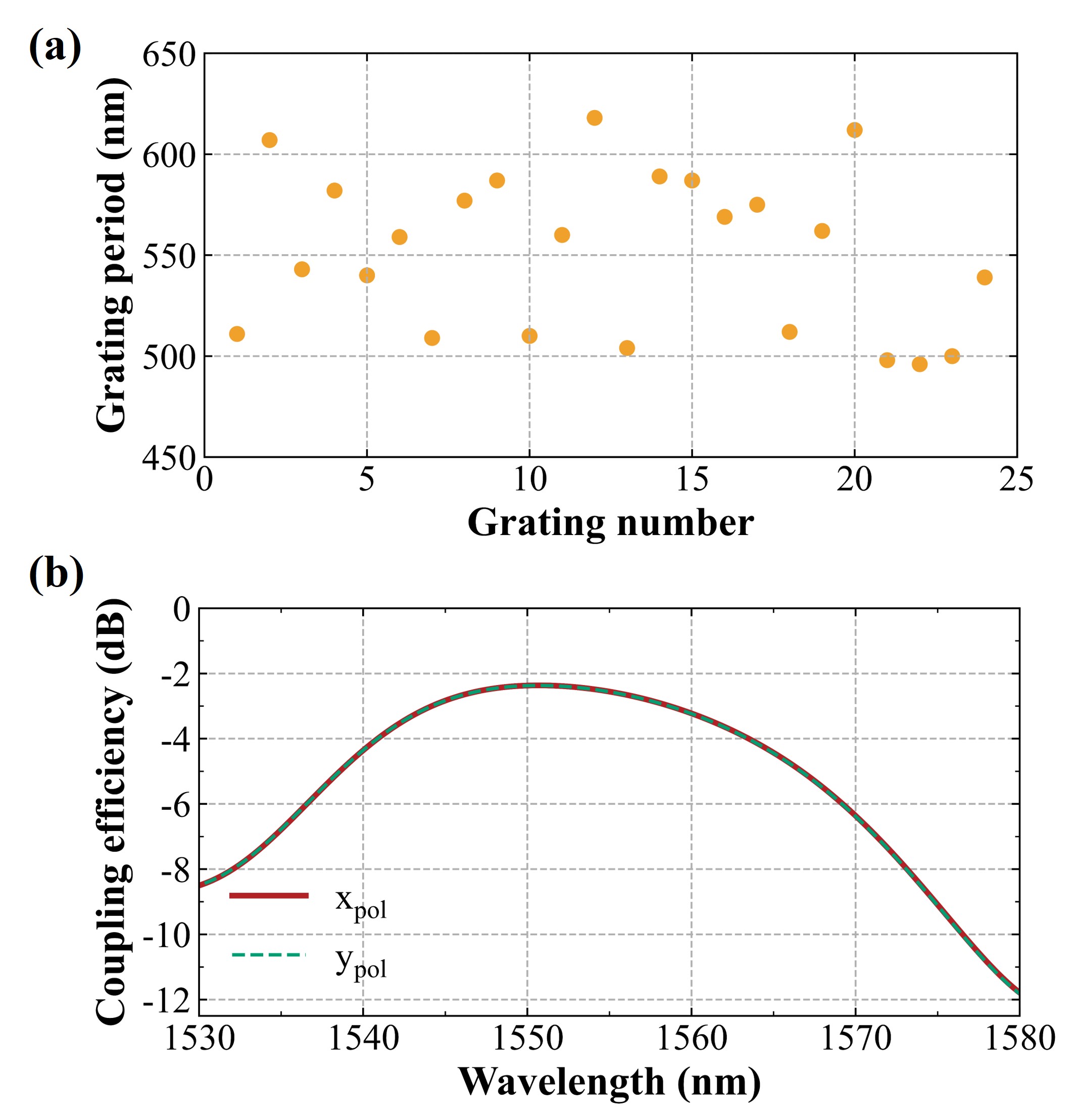
To solve this problem, we propose a novel double-layer 2D grating structure, as shown in Fig. 2(b). In our design, 70 nm deep circular holes are etched on the 220 nm Si layer, and an array of 160 nm thick aligned cylindrical teeth in poly-Si is deposited on top. The poly-Si cylindrical teeth are uniformly spaced with a consistent cylinder diameter. The shifted pattern between the two layers creates four regions of different effective refractive index, allowing optimization of the grating strength and mode overlap conditions without causing MFS issues. With the aligned double-layer structure, high directionality can also be maintained compared with the design shown in 2(a). In our design, a silicon reflector is placed at the end of the grating to enhance coupling efficiency. In addition, to enhance the coupling efficiency and reduce the second-order Bragg reflection into the waveguides due to the perfect vertical coupling configuration [30], the diameter of the nanoholes , periods of the nanoholes , widths and spacing of end reflectors, diameter of the teeth in poly-Si , and period of teeth in poly-Si , as indicated in Figure 2(b), were all optimized using a genetic algorithm and FDTD simulations [31]. Due to a large modeling area required for 3D FDTD simulations considering the optical fiber and silicon waveguide gratings, significant computational resources are needed. To mitigate this issue, we simplified the modeling using Effective Medium Theory (EMT) for 2D FDTD simulations [30]. 2D FDTD simulations can offer fast and efficient evaluation of the Figure of Merit (FOM) during the optimization iterations. As a result, the computational resources necessary for evaluating FOM are effectively reduced, enabling fast search for optimal design parameters. Fig. 3(a) illustrates the length of each grating period of the 70-nm shallowly etched holes in our final design, with an optimized etched hole diameter of 325 nm. The end reflector has a width of 365 nm with a spacing of 360 nm. For the poly-Si layer, the optimized uniform grating period is 536 nm with a teeth diameter of 300 nm. The proposed 2D grating has a total period number of 24, resulting in a grating area width of about 13.2 µm, which can achieve a good match between the diffracted optical field size and the mode field diameter of the SMF. To accurately evaluate the optimized device performance, 3D FDTD simulation is used to check the coupling efficiency spectrums for the two orthogonal polarizations. Fig. 3(b) presents the spectrum for two orthogonal polarizations when the optical signal is coupled from the optimized 2D grating coupler into a SMF. The predicted peak coupling efficiency is -2.37 dB (58%) at the wavelength of 1550 nm, with a 3-dB bandwidth of 30 nm. The symmetrical design guarantees consistent performance of the difference polarizations. It can be observed that the spectra for the two orthogonal polarizations almost overlap, indicating a small PDL of the 2D grating. Fig. 2(b) and (c) show the top view and cross-sectional optical field distribution of the 2D grating, along with the overlap between its diffracted field distribution compared with Gaussian-like fiber mode distribution. It can be found that our proposed double-layer design can successfully improve the directionality while maintaining optimal mode overlapping conditions for the two orthogonal polarizations at the same time.
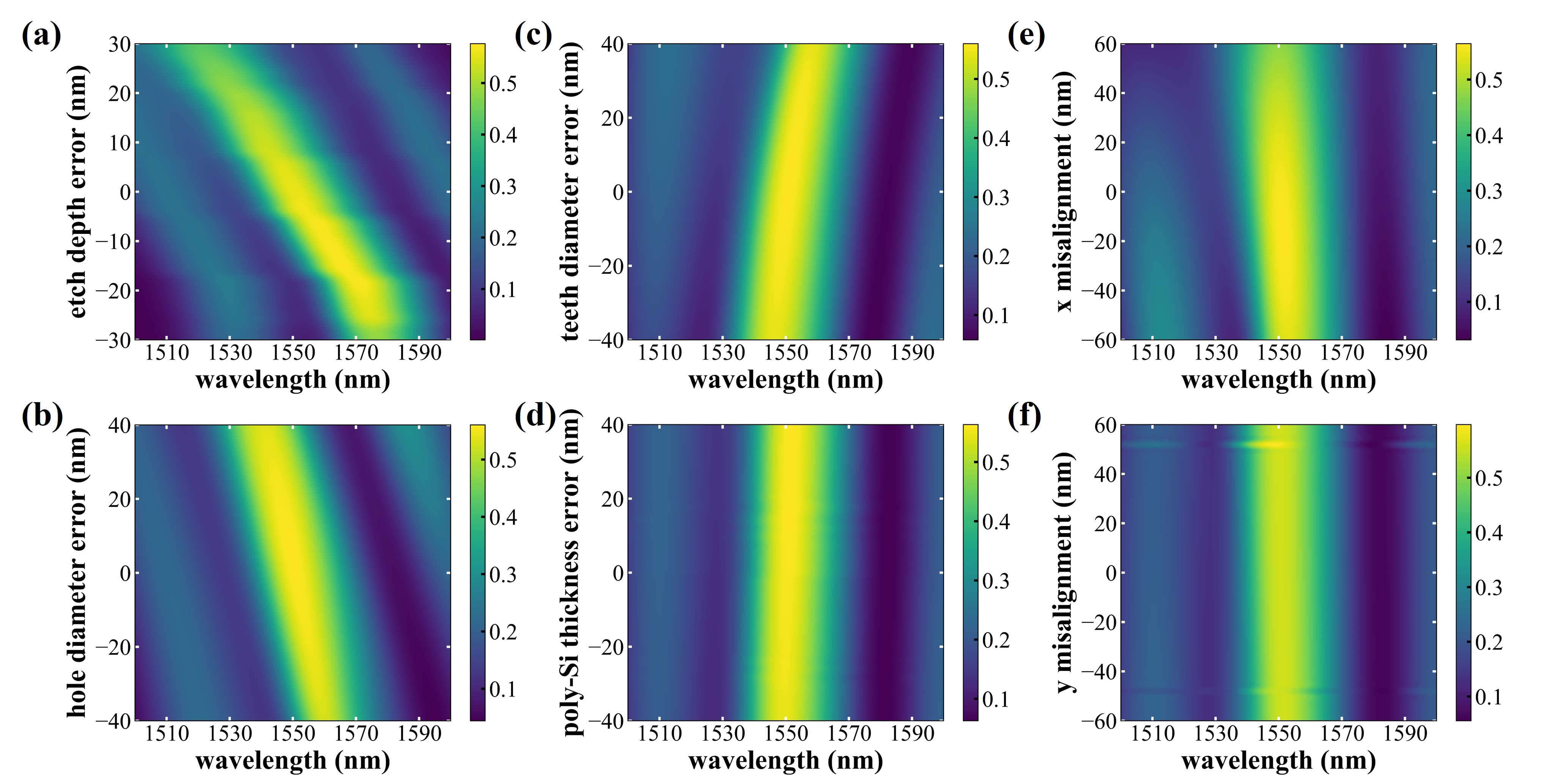
We further investigated the fabrication tolerances of our proposed double-layer 2D grating coupler, including the shallow etch depth, shallow etch size, poly-Si tooth size, poly-Si thickness, as well as the misalignment between the two layers in the x and y directions, respectively. The simulated coupling efficiency against various fabrication errors is shown in Fig. 4(a)-(f). Fig. 4(a)-(b) shows the simulated coupling efficiency versus shallow etch depth and hole size. Fabrication errors can induce wavelength shifts due to variations in the actual effective refractive index. At the wavelength of 1550 nm, even with a deviation of ±10 nm from the ideal 70 nm etch depth, the coupling efficiency remains above 50%. The device exhibits higher tolerance for the diameter of the etched holes, maintaining a coupling efficiency above 50% at 1550 nm when the fabrication error is within 20 nm. Fig. 4(c)-(d) illustrate the coupling efficiency against the poly-silicon tooth size and thickness. Variations in the thickness and size of the poly-silicon teeth within a range of ±40 nm have minimal impact on the coupling efficiency, although an increase in diameter results in a slight red shift in its peak wavelength. Fig. 4(e)-(f) depict the relationship between coupling efficiency and the misalignment between the poly-silicon layer and the shallow etch pattern in the x and y directions, respectively. The poly-silicon tooth array design provides a fabrication tolerance for misalignment in the y direction of ±60 nm and ±40 nm in the x direction.
Fabrication and Measurement
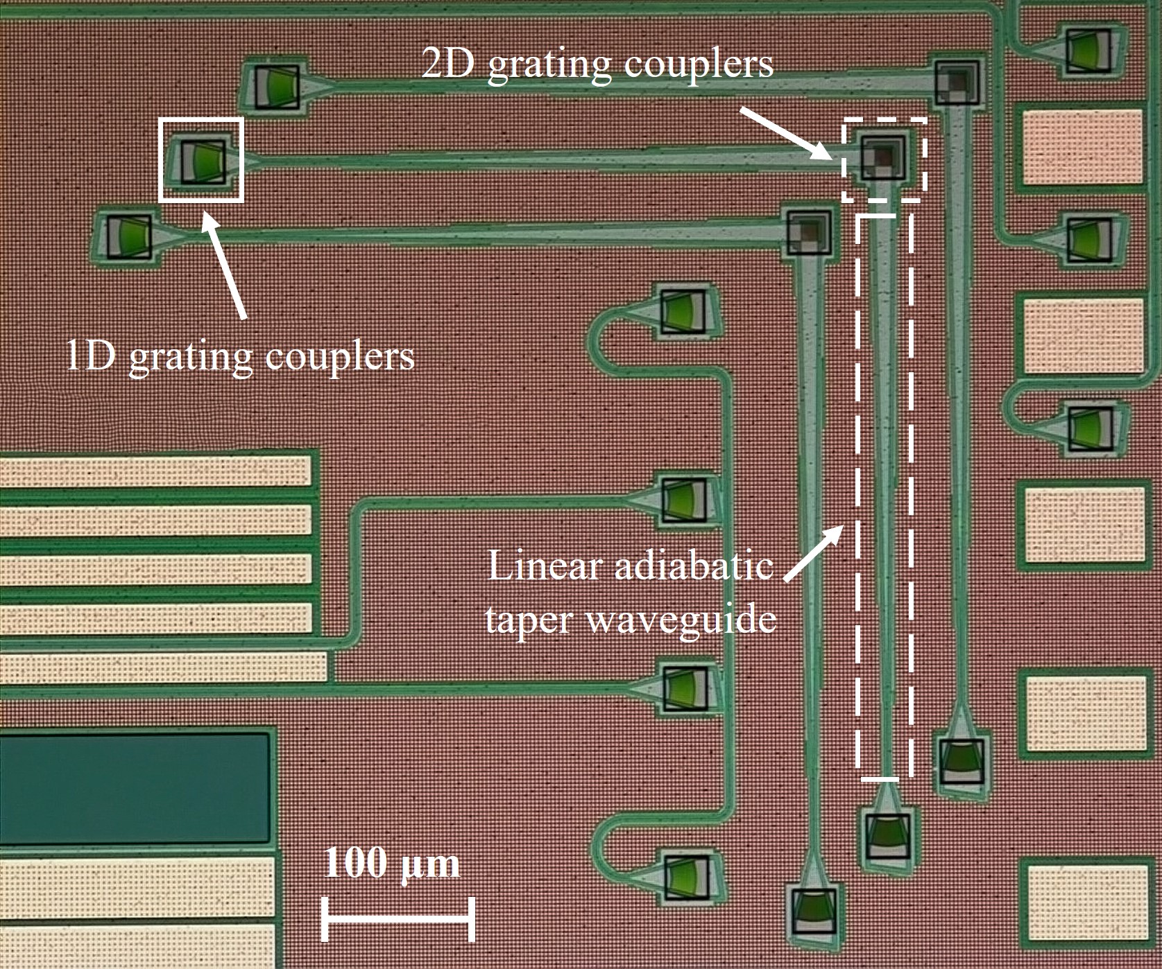
The proposed double-layer 2D grating coupler was fabricated using a multi-project wafer (MPW) run on the ISIPP50G platform provided by imec. Fig. 5 displays a microscopic image of the fabricated 2D grating coupler, which is connected to two 1D grating couplers with a coupling angle of 10°. In order to match the diffracted mode field size with the optical field in a single-mode fiber (SMF), a 360-m long linear adiabatic taper waveguide is utilized as the spot size converter.
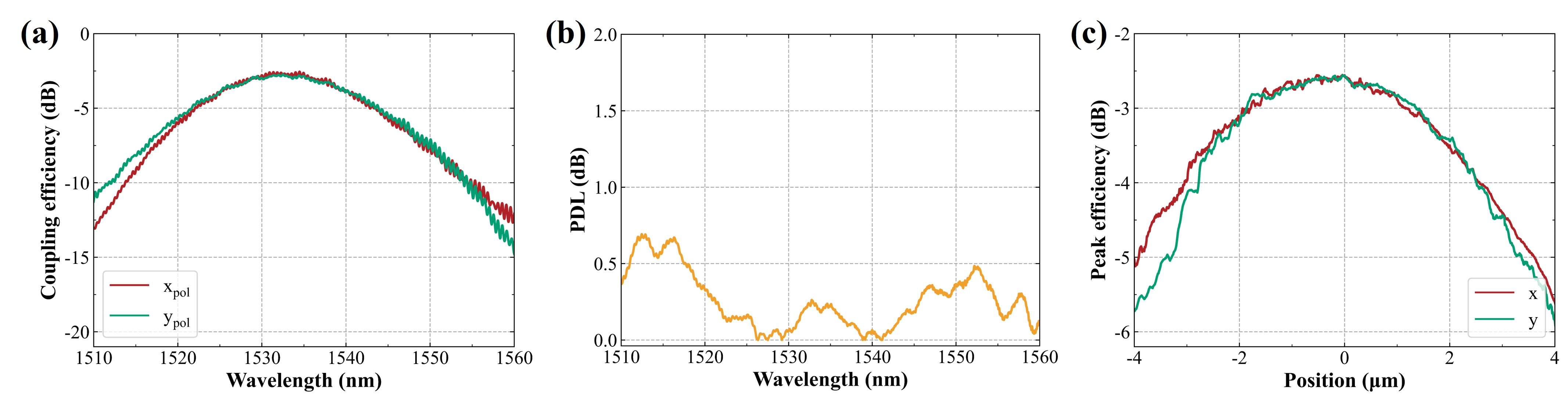
The coupling efficiency of the 2D grating coupler is characterized by measuring the fiber-chip-fiber transmission spectrum with a tunable laser source (Santec TSL-570) and an optical power meter (Santec MPM-210H and MPM-215). A three-paddle manual polarization controller (Thorlabs FPC560) is used to alter the polarization state of the optical signal in the SMF. After normalizing out the insertion loss of the 1D grating coupler, fig. 6(a) shows the coupling efficiency spectrums for the two orthogonal polarizations Ex and Ey for our proposed 2D grating coupler. A peak coupling efficiency of -2.5 dB at 1535 nm can be obtained for the x polarization. Compared to the simulation results, a small wavelength shift in the peak wavelength is observed. This deviation may arise from the fabrication uncertainties. The measured 3-dB bandwidth of the 2D grating coupler is 23.4 nm. Due to the symmetrical design for the two orthogonal polarizations, the y-polarization shows a similar peak coupling efficiency of -2.7 dB at 1531 nm. Such small discrepancies between the two polarizations are mainly due to the imperfections in the measurement alignment and fabrication process.
| Ref. | Year | WB | CA [°] | CE [dB] | CE [%] | BW [nm] | PDL [dB] | Platform | MFS [nm] |
|---|---|---|---|---|---|---|---|---|---|
| [32] | 2009 | C | 10 | -5.6 | 27% | - | >0.4 | 220 nm SOI | 180 |
| [30] | 2010 | C | 0 | -5.2 | 30% | - | <0.4 | 220 nm SOI | 195 |
| [33] | 2014 | S | 8 | -2 | 63% | 26.6∗ | - | Double SOI | - |
| [34] | 2016 | O | 6 | -3.3 | 47% | 43⋆ | <1.2 | 220 nm SOI | 180 |
| [35] | 2016 | C | 14 | -5 | 32% | - | <0.25 | 220 nm SOI | |
| [36] | 2016 | C | 14 | -3.75 | 42% | 43⋆ | - | 220 nm SOI | 272 |
| [37] | 2018 | O | 10 | -3.9 | 41% | - | <0.3 | 200 nm SOI | - |
| [21] | 2019 | C | 0 | -2.6 | 55% | 27⋆ | 3 | 220 nm SOI | 40 |
| [38] | 2019 | C | 12 | -4.2 | 38% | - | <0.2 | 220 nm SOI | 310 |
| [39] | 2020 | C | 0 | -2.5 | 56.3% | - | <0.5 | 340 nm SOI | 123 |
| [40] | 2021 | C | 10 | -4.3 | 37% | 48⋆ | <0.54 | 250 nm SOI | 187 |
| [20] | 2021 | C | 0 | -3.1 | 49% | 42∗ | <0.2 | 220 nm SOI | 180 |
| [41] | 2022 | O/C | 17 | -4.7/-8.4 | 34%/15% | 43/52⋆ | - | 340 nm SOI | 100 |
| [27] | 2022 | C | 0 | -7.0 | 20% | 89⋆ | 1.9 | GF 45SPCLO + PolySi | - |
| This work | 2024 | C | 0 | -2.54 | 56% | 23.4⋆ | <0.3 | 220 nm SOI + PolySi | 180 |
-
•
WB: wavelength band; C:1530-1565 nm; S:1460-1530 nm; O:1260-1360 nm; CA: coupling angle; CE: coupling efficiency; BW: bandwidth, ∗: 1-dB bandwidth, ⋆: 3-dB bandwidth; PDL: polarization dependent loss; MFS: minimum feature size; SOI: silicon on insulator
The PDL is also characterized by the ratio between the maximum transmission() and the minimum transmission () when varying fiber polarization across all possible states [42] as denoted by Equ. 1. In the experiment, a randomly polarized optical mode from the fiber was injected into the same 2D grating coupler, and the total transmission of the two output ports was measured.
| (1) |
Fig. 6(b) presents the spectrum of the observed PDL. Overall, the PDL is less than 0.3 dB within the 3-dB bandwidth of the 2D grating, and remains below 0.75 dB from 1510 nm to 1560 nm wavelength range. This small PDL can be attributed to the asymmetric coupling efficiency between the x-port and y-port, as well as potential measurement errors and fabrication defects given that the theoretical PDL for our design is expected to be zero.
Finally, we investigated the sensitivity of coupling efficiency versus the fiber misalignment for our 2D grating coupler. Light is sent from an SMF into the 2D grating coupler, and the optical polarization is optimized for Ex or Ey. After maximizing the coupled power by adjusting the position of the SMF, the coupling efficiency is measured against various fiber positions by a piezoelectric stage. Fig. 6(c) shows the variation of peak coupling efficiency with respect to fiber position. It can be observed that within a 2 µm positional deviation, the peak coupling efficiency remains within -3.5 dB. This indicates that the demonstrated 2D silicon grating coupler has a low alignment accuracy requirement, suggesting its potential of using a low-cost packaging process for polarization-diversity chip-fiber coupling.
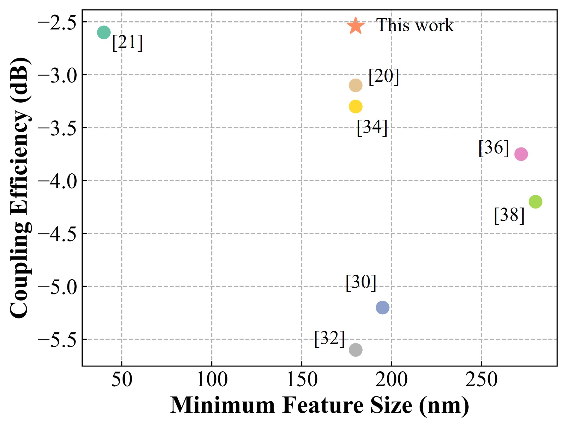
Compared with the FOMs of the 2D grating couplers reported in prior works, as summarized in Table 1, our proposed 2D grating coupler can achieve the best experimental peak coupling efficiency on the 220-nm SOI platform using a minimum feature size of 180 nm. In addition, the measured PDL can be less than 0.3 dB within its 3-dB bandwidth for future applications in the polarization-diversity photonic integrated receiver. Fig. 7 compares the peak experimental coupling efficiencies against the minimum feature sizes reported for various 2D gratings on the 220-nm SOI platform. To further improve the coupling efficiency, the poly-Si layer thickness can be optimized in the future [26] or considering incorporating additional bottom mirror [28]. Focusing 2D-grating can be utilized to further shrink the device footprint without long linear adiabatic spot size converter [42].
Conclusion
In summary, this work addresses the challenge of achieving a highly efficient and polarization-diversity fiber-chip coupling on the 220-nm SOI platform by using a novel double-layer 2D grating coupler. The demonstrated fiber-to-chip coupling efficiency can reach -2.54 dB (56%) with a minimum feature size of 180 nm, which can be fabricated using 193-nm DUV lithography. The measured experimental 3-dB bandwidth is 23.4 nm with a polarization-dependence loss <0.3 dB. Our results reveal that a high directionality and high efficiency for 2D grating couplers can be achieved by optimizing the front-end-of-line process, which can also be applied to other integrated optics platform, such as on SOI or thin-film lithium niobate platform, for polarization-diversity interface between the optical fiber and the photonic integrated circuits.
Acknowledgements: The authors acknowledge the Novel IC Exploration (NICE) Facility of HKUST(GZ) for technical support and imec for photonic integrated circuits fabrication. This work was funded by the Natural Science Foundation of Guangdong Province (No.2024A1515012438), Department of Education of Guangdong Province (No. 2023KTSCX167), Guangzhou Association for Science and Technology (No. QT2024-011), and Guangzhou Municipal Science and Technology Project (No.2023A03J0013).
References
- [1] Xiang, C., Bowers, S. M., Bjorlin, A., Blum, R. & Bowers, J. E. Perspective on the future of silicon photonics and electronics. Applied Physics Letters 118 (2021).
- [2] Wade, M. et al. An error-free 1 tbps wdm optical i/o chiplet and multi-wavelength multi-port laser. In Optical Fiber Communication Conference, F3C–6 (Optica Publishing Group, 2021).
- [3] Shi, Y. et al. Silicon photonics for high-capacity data communications. Photonics Research 10, A106–A134 (2022).
- [4] Bogaerts, W. et al. Programmable photonic circuits. Nature 586, 207–216 (2020).
- [5] Lu, K. et al. Empowering high-dimensional optical fiber communications with integrated photonic processors. Nature Communications 15, 3515 (2024).
- [6] Zhou, H. et al. Self-configuring and reconfigurable silicon photonic signal processor. Acs Photonics 7, 792–799 (2020).
- [7] Sun, J., Timurdogan, E., Yaacobi, A., Hosseini, E. S. & Watts, M. R. Large-scale nanophotonic phased array. Nature 493, 195–199 (2013).
- [8] Rogers, C. et al. A universal 3d imaging sensor on a silicon photonics platform. Nature 590, 256–261 (2021).
- [9] Marchetti, R., Lacava, C., Carroll, L., Gradkowski, K. & Minzioni, P. Coupling strategies for silicon photonics integrated chips. Photonics Research 7, 201–239 (2019).
- [10] Kopp, C. et al. Silicon photonic circuits: on-cmos integration, fiber optical coupling, and packaging. IEEE Journal of selected topics in quantum electronics 17, 498–509 (2010).
- [11] Benedikovic, D. et al. L-shaped fiber-chip grating couplers with high directionality and low reflectivity fabricated with deep-uv lithography. Optics Letters 42, 3439–3442 (2017).
- [12] Benedikovic, D. et al. High-directionality fiber-chip grating coupler with interleaved trenches and subwavelength index-matching structure. Optics Letters 40, 4190–4193 (2015).
- [13] Cheng, Z. & Tsang, H. K. Experimental demonstration of polarization-insensitive air-cladding grating couplers for silicon-on-insulator waveguides. Optics Letters 39, 2206–2209 (2014).
- [14] Mak, J. C. et al. Multi-layer silicon nitride-on-silicon polarization-independent grating couplers. Optics express 26, 30623–30633 (2018).
- [15] Wang, Y. et al. Apodized focusing fully etched subwavelength grating couplers. IEEE Photonics Journal 7, 1–10 (2015).
- [16] Taillaert, D. et al. A compact two-dimensional grating coupler used as a polarization splitter. IEEE Photonics Technology Letters 15, 1249–1251 (2003).
- [17] Bogaerts, W. et al. A polarization-diversity wavelength duplexer circuit in silicon-on-insulator photonic wires. Optics express 15, 1567–1578 (2007).
- [18] Doerr, C. R. et al. Monolithic polarization and phase diversity coherent receiver in silicon. Journal of lightwave technology 28, 520–525 (2010).
- [19] Rahim, A. et al. Open-access silicon photonics platforms in europe. IEEE Journal of Selected Topics in Quantum Electronics 25, 1–18 (2019).
- [20] Zhang, Z. et al. High-efficiency two-dimensional perfectly vertical grating coupler with ultra-low polarization dependent loss and large fibre misalignment tolerance. IEEE Journal of Quantum Electronics 57, 1–7 (2021).
- [21] Watanabe, T., Fedoryshyn, Y. & Leuthold, J. 2-d grating couplers for vertical fiber coupling in two polarizations. IEEE Photonics Journal 11, 1–9 (2019).
- [22] Sacher, W. D. et al. Wide bandwidth and high coupling efficiency si 3 n 4-on-soi dual-level grating coupler. Optics express 22, 10938–10947 (2014).
- [23] Sacher, W. D. et al. Monolithically integrated multilayer silicon nitride-on-silicon waveguide platforms for 3-d photonic circuits and devices. Proceedings of the IEEE 106, 2232–2245 (2018).
- [24] Tong, Y., Zhou, W. & Tsang, H. K. Efficient perfectly vertical grating coupler for multi-core fibers fabricated with 193 nm duv lithography. Optics Letters 43, 5709–5712 (2018).
- [25] Pantouvaki, M. et al. Active components for 50 gb/s nrz-ook optical interconnects in a silicon photonics platform. Journal of lightwave technology 35, 631–638 (2016).
- [26] Carroll, L., Gerace, D., Cristiani, I. & Andreani, L. C. Optimizing polarization-diversity couplers for si-photonics: reaching the- 1db coupling efficiency threshold. Optics express 22, 14769–14781 (2014).
- [27] Hammond, A. M., Slaby, J. B., Probst, M. J. & Ralph, S. E. Multi-layer inverse design of vertical grating couplers for high-density, commercial foundry interconnects. Optics Express 30, 31058–31072 (2022).
- [28] Luo, Y. et al. Low-loss two-dimensional silicon photonic grating coupler with a backside metal mirror. Optics Letters 43, 474–477 (2018).
- [29] Chen, X., Li, C., Fung, C. K., Lo, S. M. & Tsang, H. K. Apodized waveguide grating couplers for efficient coupling to optical fibers. IEEE Photonics Technology Letters 22, 1156–1158 (2010).
- [30] Chen, X., Li, C. & Tsang, H. K. Two dimensional silicon waveguide chirped grating couplers for vertical optical fibers. Optics Communications 283, 2146–2149 (2010).
- [31] Tong, Y., Zhou, W., Wu, X. & Tsang, H. K. Efficient mode multiplexer for few-mode fibers using integrated silicon-on-insulator waveguide grating coupler. IEEE Journal of Quantum Electronics 56, 1–7 (2020).
- [32] Van Laere, F. et al. Focusing polarization diversity grating couplers in silicon-on-insulator. Journal of Lightwave Technology 27, 612–618 (2009).
- [33] Verslegers, L. et al. Design of low-loss polarization splitting grating couplers. In Integrated Photonics Research, Silicon and Nanophotonics, JT4A–2 (Optica Publishing Group, 2014).
- [34] Wu, W., Lin, T., Chu, T. & Zhang, H. Cmos-compatible high efficiency polarization splitting grating coupler near 1310nm. In Asia Communications and Photonics Conference, AS2F–4 (Optica Publishing Group, 2016).
- [35] Zou, J., Yu, Y. & Zhang, X. Two-dimensional grating coupler with a low polarization dependent loss of 0.25 db covering the c-band. Opt. Lett. 41, 4206–4209 (2016).
- [36] Lacava, C. et al. Design and characterization of low-loss 2d grating couplers for silicon photonics integrated circuits. In Silicon Photonics XI, vol. 9752, 125–131 (SPIE, 2016).
- [37] Sobu, Y., Jeong, S.-H. & Tanaka, Y. Si-wire two-dimensional grating coupler with polarization-dependent loss of lower than 0.3 db over a 60-nm-wide spectral range. Japanese Journal of Applied Physics 57, 112501 (2018).
- [38] Xue, Y., Chen, H., Bao, Y., Dong, J. & Zhang, X. Two-dimensional silicon photonic grating coupler with low polarization-dependent loss and high tolerance. Optics express 27, 22268–22274 (2019).
- [39] Zhang, Z. et al. Two-dimensional apodized grating coupler for polarization-independent and surface-normal optical coupling. Journal of Lightwave Technology 38, 4037–4044 (2020).
- [40] Ruiz, J. L. P. et al. Compact dual-polarization silicon integrated couplers for multicore fibers. Optics letters 46, 3649–3652 (2021).
- [41] Cheng, G. et al. Single-step etched two-dimensional polarization splitting dual-band grating coupler for wavelength (de) multiplexing. Optics Letters 47, 3924–3927 (2022).
- [42] Van Laere, F. et al. Focusing polarization diversity grating couplers in silicon-on-insulator. Journal of Lightwave Technology 27, 612–618 (2009).