Sliding-Reversible Bandgap Modulation in Irreversible Asymmetric Multilayers
Abstract
The electronic bandgap of a material is often fixed after fabrication. The capability to realize on-demand and non-volatile control over the bandgap will unlock exciting opportunities for adaptive devices with enhanced functionalities and efficiency. We introduce a general design principle for on-demand and non-volatile control of bandgap values, which utilizes reversible sliding-induced polarization driven by an external electric field to modulate the irreversible background polarization in asymmetric two-dimensional (2D) multilayers. The structural asymmetry can be conveniently achieved in homobilayers of Janus monolayers and heterobilayers of nonpolar monolayers, making the design principle applicable to a broad range of 2D materials. We demonstrate the versatility of this design principle using experimentally synthesized Janus metal dichalcogenide (TMD) multilayers as examples. Our first-principles calculations show that the bandgap modulation can reach up to 0.3 eV and even support a semimetal-to-semiconductor transition. By integrating a ferroelectric monolayer represented by 1T′′′-MoS2 into a bilayer, we show that the combination of intrinsic ferroelectricity and sliding ferroelectricity leads to multi-bandgap systems coupled to multi-step polarization switching. The sliding-reversible bandgap modulation offers an avenue to dynamically adjust the optical, thermal, and electronic properties of 2D materials through mechanical and electrical stimuli.
Institute of Natural Sciences, Westlake Institute for Advanced Study, Hangzhou, Zhejiang 310024, China \alsoaffiliationInstitute of Natural Sciences, Westlake Institute for Advanced Study, Hangzhou, Zhejiang 310024, China \alsoaffiliationInstitute of Natural Sciences, Westlake Institute for Advanced Study, Hangzhou, Zhejiang 310024, China \alsoaffiliationInstitute of Natural Sciences, Westlake Institute for Advanced Study, Hangzhou, Zhejiang 310024, China
1 Introduction
The bandgap, a fundamental property of materials, is crucial in determining their optical, thermal, and electrical behaviors 1. It holds a key role in modern device physics and technology, determining the performance of a wide range of devices like transistors, solar cells, and light-emitting diodes 2, 3, 4, 5. The ability to dynamically and non-volatilely adjust the bandgap is highly desirable, enabling real-time control of material properties. This opens up opportunities for “smart devices” that respond instantaneously to changes in environmental conditions or user inputs, thereby enhancing both functionality and efficiency 6. For example, solar panels with tunable bandgaps could optimize their absorption characteristics to maximize efficiency throughout the day and in various weather conditions. Materials with temperature-sensitive bandgaps that regulate light and heat transmission in response to changing environmental conditions form the basis of smart windows 6. Similarly, tunable laser diodes that allow on-demand control of their output wavelength may provide enhanced precision in procedures like laser surgery or scanning 7. While techniques like doping 8, 5, strain 9, and interface engineering 10 can effectively modify material bandgaps, these methods are typically static, meaning the bandgap is fixed after fabrication. This poses a challenge for achieving dynamic and real-time control over bandgaps. Efforts for reversible bandgap tuning have mainly focused on phase-change materials 11, 12 and electric field effect 13, 14. However, materials that exhibit robust, dynamic, and non-volatile bandgap tunability are still relatively rare.
Two-dimensional (2D) van der Waals (vdW) materials can be stacked and relatively shifted. The interlayer motions like sliding and twisting offer a unique degree of freedom to tune the properties of these material, even inducing emergent phenomena not present in their individual layers 15, 16, 17, 18, 19. For example, controlling the twist angle between layers can lead to the formation of long-wavelength moiré potential, effectively quenching the kinetic energy of electrons and enhance the electronic correlation. This sets the stage for various exotic quantum phases, such as superconductivity 20, 21, 22 and Mott insulators 23, 24, 25. In recent years, sliding ferroelectricity, a phenomenon where lateral sliding between nonpolar monolayers produces a switchable vertical polarization, has attracted great attention. Notable bilayer systems exhibiting sliding ferroelectricity that have been confirmed experimentally include bilayer boron nitride and transition metal dichalcogenides 26, 15, 27, 28, 29. This discovery expands the range of 2D ferroelectrics with out-of-plane polarization, potentially allowing for full utilization of atomic thickness in the development of ultrathin nanoelectronics. Various measures can induce interlayer sliding in layered vdW materials, including external electric field 30, 26, 15 and shear strain 31.
Given the facile capability to induce interlayer sliding, sliding-induced bandgap modulation, if achievable, could significantly improve the methods available for real-time tuning of electronic structures. However, unlike twisting, sliding in bilayers of identical monolayers generally has a less significant impact on their electronic properties, as it doesn’t substantially modulate the periodic potential landscape. Here, we present a general strategy that integrates a reversible polarization arsing from sliding () with a background out-of-plane polarization () that does not need to be reversible (switchable), to achieve sliding-tunable bandgaps in a vdW multilayer.
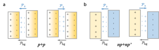
Taking a bilayer as an example (Fig. 1), the background polarization may result from the structural asymmetry of the monolayer, such as in a homobilayer of Janus materials. It could also arise from charge transfer between nonpolar monolayers with different work functions in a heterobilayer. In both cases, the direction of is not reversible by an electric field. Another key requirement for the bilayer configuration is that it should support sliding ferroelectricity, which can be conveniently achieved based on the general theory for bilayer stacking ferroelectricity 32. For a bilayer with both and , the sliding allows the transition between two states with different out-of-plane polarization, a high-polarization (HP) state with and a low-polarization (LP) state with . Since the depolarization field within the bilayer is directly coupled to the magnitude of the out-of-plane polarization and can strongly affect the band gap 33, 34, 35, the two polar states can possess substantially different bandgaps, enabling sliding-induced, nonvolatile tuning of the electronic structures.
We demonstrate this design principle using density functional theory (DFT) calculations, focusing on the well-known family of 2D materials, transition metal dichalcogenides (TMDs) 36, 37, many of which have already been synthesized experimentally. We find that a Janus 1H- ( = Mo, W; = S, Se, Te) bilayer with parallel stacking, denoted as the configuration (Fig. 1a), can exhibit a reversible bandgap change of 0.1–0.2 eV. Moreover, a sliding-driven semimetal-semiconductor transition is realized in the 1T-WTeSe bilayer. Additionally, the magnitude of bandgap modulation can be further enhanced with increasing layer number. Specifically, the sliding-induced bandgap change in the trilayer 1H-WTeSe reaches up to 0.3 eV. The design principle is also applicable to a heterobilayer consisting of nonpolar monolayers, denoted as (Fig. 1b), as exemplified by 1H-WSe2/1H-Mo ( = S, Se, Te). Finally, we show that in a bilayer consisting of recently synthesized ferroelectric 1T′′′-MoS2 and nonpolar 1H-MoS2 ( configuration), it is possible to achieve a multi-bandgap system coupled to multistep polarization switching. The design principle proposed in this work for on-demand control of bandgaps is versatile and opens up opportunities for voltage-configurable multi-state electronics.
2 Methods
DFT calculations are performed using the Vienna ab initio Simulation Package VASP 38, 39. The exchange-correlation interaction is described by the Perdew–Burke–Ernzerhof (PBE) functional 40 and Heyd-Scuseria-Ernzerhof hybrid density functional (HSE06) 41, with Grimme’s D3 dispersion correction 42. The projector augmented wave (PAW) method 43 is used to describe the electron-ion interaction between the core ion and valence electrons. The plane-wave kinetic energy cutoff is 600 eV, and a 991 Monkhorst-Pack grid is used to sample the Brillouin zone for the unit cell. A vacuum region of more than 20 Å thick is included to avoid interactions between periodic images. The climbing image nudged elastic band (CL-NEB) method 44 is employed to identify minimum energy pathways, with electronic energy and atomic force converged to 10-7 eV and 0.01 eV/Å, respectively. Dipole correction is considered in all calculations.
3 Results and Discussion
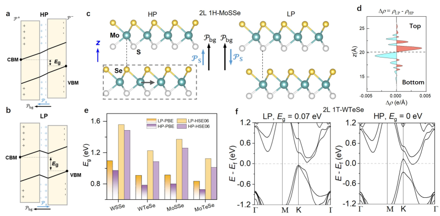
stackingWe start with a heuristic approach to understand the bandgap modulation caused by the interlayer sliding in a homobilayer consisting of two polar Janus monolayers. As depicted in Fig. 2a, the surface polarization bound charges associated with the out-of-plane polarization generates a depolarization field that opposes the polarization. This field establishes a potential step that scales with the magnitude of the polarization, thereby differentiating the electronic states of the two polar surfaces. Electrons near the surface naturally have higher energies due to increased Coulomb repulsion, which defines the valence band maximum (VBM). Conversely, the conduction band minimum (CBM) is located at the surface. The depolarization field resembles the built-in electric field within the depletion region of a – junction. Although the polarization direction of Janus monolayers, , are not reversible, the polarization arsing from the stacking, , can be flipped by sliding. Therefore, the effective potential step across the bilayer in the HP state with is higher than that in the LP state with . This results in a larger bandgap in the LP state.
The simple band bending model discussed above is corroborated by our DFT calculations of 2D Janus TMDs, many of which, like MoSeS and WSeS, have already been synthesized 45, 46. As a case study, we focus on the 1H-MoSSe bilayer. In the AB-stacking configuration, as illustrated in Fig. 2c, electrons transfer from the upper Mo layer to the lower Se layer due to the greater electronegativity of Se relative to Mo. This leads to an upward that runs along and thus a HP state. Band structure calculations with PBE reveal a bandgap of eV. Sliding the bottom layer by 1/3 of a unit cell reverses the charge transfer direction (see Fig. 2d), resulting in a LP state and a higher bandgap of eV. Therefore, a bandgap modulation = 0.1 eV is achieved in the 1H-MoSSe bilayer. We further perform calculations for 1H-WSSe, WTeSe, MoSSe, and MoTeSe bilayers, with the bandgap values computed with PBE and HSE06 reported in Fig. 2e. It is evident that the bandgap modulation driven by the sliding is a robust phenomenon common to all studied bilayers. Besides the 1H phase with trigonal prismatic coordination, 2D TMDs may also crystallize in the 1T phase featuring the tetragonal symmetry and octahedral coordination of the transition metal. Interestingly, we find that the bilayer 1T-WTeSe undergoes a semiconductor-to-semimetal transition during the sliding from a LP state to a HP state, as depicted in Fig. 2f.
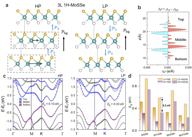
The magnitude of can be enhanced in multilayers by promoting the contribution of reversible to the total polarization. For a trilayer 1H-MoSSe, it may adopt “ladder ferroelectricity” where each pair of neighboring monolayers supports stacking ferroelectricity 47. As illustrated in Fig. 3a, an ABC stacked trilayer has two interfaces possessing parallel upward . Applying a sliding gradient, where the middle layer slides one-third of a unit cell and the bottom layer slides two-thirds of a unit cell, will change the stacking from ABC to CBA, switching the direction of at both interfaces and resulting in a LP state (see the change in charge density in Fig. 3b). Our DFT calculations confirm that the ABC configuration, characterized by an out-of-plane polarization of 18.6 pC/m, has a PBE band gap of 0.13 eV. In contrast, the polarization in the CBA-stacked trilayer decreases to 16.7 pC/m, and the bandgap widens to 0.33 eV. The magnitude of in this trilayer is 0.2 eV, doubling the 0.1 eV observed in the bilayer. Additionally, the atom-resolved band structures (Fig. 3c) confirm that the VBM and CBM are dominated by states of the bottom layer and the top layer, respectively, consistent with the schematic illustrated in Fig. 2a and b. As summarized in Fig 3d for several Janus trilayers, the value of ranges from 0.2 to 0.3 eV, improving upon those in bilayers. Specifically, HSE06 predicts a bandgap modulation of 0.3 eV and a direct-to-indirect bandgap transition in the trilayer 1H-WTeSe.
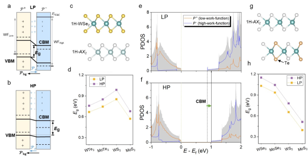
+ stackingThe proposed design principle does not rely on polar monolayers for two reasons. First, the work function difference between the constituent monolayers in a heterobilayer can serve as the origin of . Second, a distinct feature of sliding ferroelectrics is that the stacking of nonpolar monolayers can also generate vertical polarization as long as the stacking satisfies the symmetry requirement 32. The mechanism of bandgap modulation in an + heterobilayer is sketched in Fig. 4a and b, which differs subtly from the + stacking. The charge transfer between monolayers pushes down the valence states in the low-work-function layer and raises the conduction states in the high-work-function layer. Since the VBM and CBM are located in the low-work-function and high-work-function layers, respectively, stronger charge transfer causes the VBM and CBM to move further apart. In the LP state, the sliding induced tends to suppress charge transfer between monolayers, leading to a smaller bandgap. Conversely, in the HP state where promotes the charge transfer, the bandgap is larger. It is important to note that the correlation between and the magnitude of total polarization is exactly opposite to that in homobilayers of the configuration.
Our DFT investigations of 1H-WSe2/1H- ( Mo, W; S, Se, Te) bilayers confirm the model analysis discussed above, revealing that the HP state indeed has a larger bandgap, with the values of range from 0.09 to 0.14 eV, as shown in Fig. 4d. The projected density of states (PDOS) diagrams in Fig. 4e and f for 1H-WSe2/1H-WS2 heterobilayer show a clear upward shift of the CBM of the high-work-function layer in HP states, consistent with schematics in Fig. 4a and b.
A potential issue for a hetrobilayer is the lattice mismatch-induce formation of moiré patterns, which could complicate the control over sliding ferroelectricity. We suggest that doping presents a viable solution to mitigate the mismatch and enhance control. For instance, the lattice mismatch between 1H-WTe2 (with an in-plane lattice constant 3.52 Å) and 1H-WSe2 ( 3.30 Å) can be significantly reduced by doping 1H-WSe2 with Te atoms ( 3.40 Å). This doping approach is feasible, as our design principle does not require an ordered arrangement of Te dopants within the lattice. We perform a set of model calculations for 1H-/1H- ( Mo, W; S, Se), where 1H- approximates a (homogeneously) Te-doped nonpolar monolayer (Fig. 4g, not a polar Janus monolayer). Similar to the undoped heterobilayer, the HP state consistently exhibits a larger bandgap than the LP state (Fig. 4h), further confirming the robustness of the design principle.
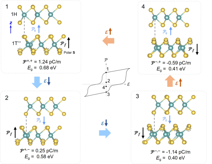
+ configurationReversible and precisely tunable multistate switching is essential for enabling high-density information storage and neuromorphic computing applications 48, 49.Finally, we demonstrate that combining a 2D ferroelectric with a nonpolar monolayer (denoted as +) presents a compelling route to achieve fine-tuned and non-volatile control over multiple bandgaps using voltage. In this bilayer, there are three types of polarization: originating from monolayer’s ferroelectricity, due to the work function difference, and arising from sliding ferroelectricity. This leads to four polar states in this bilayer system: , , , and , labeled as , , , and , respectively. We focus on a possible experimental realization of such a bilayer system, specifically a 1H-MoS2/1T′′′-MoS2 heterojunction. It is noted that 1T′′′-MoS2 featuring a switchable out-of-plane polarization has been experimentally synthesized recently 50. The minimum energy pathways for the reversal processes of and are identified using the DFT-based NEB technique, respectively. The barrier for switching is 0.043 eV/atom, higher than the 0.012 eV/atom required for switching . This difference likely translates to multi-step polarization switching under an applied electric field (). Starting at the state, the bandgap evolves from 0.68 eV to 0.58 eV at the partially switched state, and then becomes 0.40 eV at the fully reversed state (Fig. 5). Applying an opposite electric field can recover the state eventually. The multi-step polarization switching under an applied electric field, coupled to the corresponding changes in multiple bandgap values, highlights the potential for developing multistate memory devices.
4 Conclusion
In summary, we have demonstrated a general design principle to realize reversible and non-volatile bandgap modulation by taking advantage of both sliding ferroelectricity and structural asymmetry in 2D multilayers. The irreversible background polarization arising from the structural asymmetry is modulated by the reversible polarization due to sliding, leading to polar states with different polarization magnitudes and thereby varying built-in depolarization fields that strongly affect the electronic structures. A notable advantage of this design principle is that it is applicable to both homobilayers of polar monolayers as well as heterobilayers of nonpolar monolayers. Based on experimentally synthesized 2D Janus materials, we demonstrate substantial bandgap modulations up to 0.3 eV. The introduction of ferroelectric monolayer such as 1T′′′-MoS2 into a bilayer to enable switchable background polarization allow for on-demand control of multiple bandgap values via voltage, offering exciting opportunities for adaptive electronics and multistate memory.
5 Acknowledgments
This work is supported by National Natural Science Foundation of China (12304128,12074319) and Westlake Education Foundation. The computational resource is provided by Westlake HPC Center.
References
- Ashcroft and Mermin 1976 Ashcroft, N. W.; Mermin, N. D. Solid State Physics; Brooks Cole, 1976
- Sze and Ng 2006 Sze, S. M.; Ng, K. K. Physics of semiconductor devices; John Wiley & Sons, Ltd, 2006
- Chaves et al. 2020 Chaves, A.; Azadani, J. G.; Alsalman, H.; da Costa, D. R.; Frisenda, R.; Chaves, A. J.; Song, S. H.; Kim, Y. D.; He, D.; Zhou, J.; Castellanos-Gomez, A.; Peeters, F. M.; Liu, Z.; Hinkle, C. L.; Oh, S.-H.; Ye, P. D.; Koester, S. J.; Lee, Y. H.; Avouris, P.; Wang, X.; Low, T. Bandgap engineering of two-dimensional semiconductor materials. npj 2D Mater. Appl. 2020, 4, 29
- Varley et al. 2022 Varley, J. B.; Shen, B.; Higashiwaki, M. Wide bandgap semiconductor materials and devices. J. Appl. Phys. 2022, 131, 230401
- Ning et al. 2017 Ning, C.-Z.; Dou, L.; Yang, P. Bandgap engineering in semiconductor alloy nanomaterials with widely tunable compositions. Nat. Rev. Mater. 2017, 2, 17070
- Zhou et al. 2021 Zhou, Y.; Fan, F.; Liu, Y.; Zhao, S.; Xu, Q.; Wang, S.; Luo, D.; Long, Y. Unconventional smart windows: Materials, structures and designs. Nano Energy 2021, 90, 106613
- Buus et al. 2005 Buus, J.; Amann, M.-C.; BlumenthalSze, D. J. Tunable Laser Diodes and Related Optical Sources; Wiley-IEEE Press, 2005
- Chen et al. 2013 Chen, Y.; Xi, J.; Dumcenco, D. O.; Liu, Z.; Suenaga, K.; Wang, D.; Shuai, Z.; Huang, Y.-S.; Xie, L. Tunable Band Gap Photoluminescence from Atomically Thin Transition-Metal Dichalcogenide Alloys. ACS Nano 2013, 7, 4610–4616
- Lee et al. 2004 Lee, M. L.; Fitzgerald, E. A.; Bulsara, M. T.; Currie, M. T.; Lochtefeld, A. Strained Si, SiGe, and Ge channels for high-mobility metal-oxide-semiconductor field-effect transistors. J. Appl. Phys. 2004, 97, 011101
- Kroemer 2001 Kroemer, H. Nobel Lecture: Quasielectric fields and band offsets: teaching electrons new tricks. Rev. Mod. Phys. 2001, 73, 783–793
- Dong et al. 2019 Dong, W.; Liu, H.; Behera, J. K.; Lu, L.; Ng, R. J. H.; Sreekanth, K. V.; Zhou, X.; Yang, J. K. W.; Simpson, R. E. Wide Bandgap Phase Change Material Tuned Visible Photonics. Adv. Funct. Mater. 2019, 29, 1806181
- Prabhathan et al. 2023 Prabhathan, P.; Sreekanth, K. V.; Teng, J.; Ko, J. H.; Yoo, Y. J.; Jeong, H.-H.; Lee, Y.; Zhang, S.; Cao, T.; Popescu, C.-C.; Mills, B.; Gu, T.; Fang, Z.; Chen, R.; Tong, H.; Wang, Y.; He, Q.; Lu, Y.; Liu, Z.; Yu, H.; Mandal, A.; Cui, Y.; Ansari, A. S.; Bhingardive, V.; Kang, M.; Lai, C. K.; Merklein, M.; Song, Y. M.; Tian, Z.; Hu, J.; Losurdo, M.; Majumdar, A.; Miao, X.; Chen, X.; Gholipour, B.; Richardson, K. A.; Eggleton, B. J.; Wuttig, M.; Singh, R. Roadmap for phase change materials in photonics and beyond. iScience 2023, 26, 107946
- Zhang et al. 2009 Zhang, Y.; Tang, T.-T.; Girit, C.; Hao, Z.; Martin, M. C.; Zettl, A.; Crommie, M. F.; Shen, Y. R.; Wang, F. Direct observation of a widely tunable bandgap in bilayer graphene. Nature 2009, 459, 820–823
- Castro et al. 2007 Castro, E. V.; Novoselov, K. S.; Morozov, S. V.; Peres, N. M. R.; Guinea, F.; Geim, A. K.; Neto, A. H. C. Biased Bilayer Graphene: Semiconductor with a Gap Tunable by the Electric Field Effect. Phys. Rev. Lett. 2007, 99, 216802
- Stern et al. 2021 Stern, M. V.; Waschitz, Y.; Cao, W.; Nevo, I.; Watanabe, K.; Taniguchi, T.; Sela, E.; Urbakh, M.; Hod, O.; Shalom, M. B. Interfacial ferroelectricity by van der Waals sliding. Science 2021, 372, 1462–1466
- Wu and Li 2021 Wu, M.; Li, J. Sliding ferroelectricity in 2D van der Waals materials: Related physics and future opportunities. Proc. Natl. Acad. Sci. U.S.A. 2021, 118, e2115703118
- Cui et al. 2020 Cui, T.; Yip, K.; Hassan, A.; Wang, G.; Liu, X.; Sun, Y.; Filleter, T. Graphene fatigue through van der Waals interactions. Sci. Adv. 2020, 6, eabb1335
- Pakdel et al. 2024 Pakdel, S.; Rasmussen, A.; Taghizadeh, A.; Kruse, M.; Olsen, T.; Thygesen, K. S. High-throughput computational stacking reveals emergent properties in natural van der Waals bilayers. Nat. Commun. 2024, 15, 932
- Ding et al. 2021 Ding, N.; Chen, J.; Gui, C.; You, H.; Yao, X.; Dong, S. Phase competition and negative piezoelectricity in interlayer-sliding ferroelectric ZrI2. Phys. Rev. Mater. 2021, 5, 084405
- Cao et al. 2018 Cao, Y.; Fatemi, V.; Fang, S.; Watanabe, K.; Taniguchi, T.; Kaxiras, E.; Jarillo-Herrero, P. Unconventional superconductivity in magic-angle graphene superlattices. Nature 2018, 556, 43–50
- Chen et al. 2019 Chen, G.; Sharpe, A. L.; Gallagher, P.; Rosen, I. T.; Fox, E. J.; Jiang, L.; Lyu, B.; Li, H.; Watanabe, K.; Taniguchi, T.; Jung, J.; Shi, Z.; Goldhaber-Gordon, D.; Zhang, Y.; Wang, F. Signatures of tunable superconductivity in a trilayer graphene moiré superlattice. Nature 2019, 572, 215–219
- Yankowitz et al. 2019 Yankowitz, M.; Chen, S.; Polshyn, H.; Zhang, Y.; Watanabe, K.; Taniguchi, T.; Graf, D.; Young, A. F.; Dean, C. R. Tuning superconductivity in twisted bilayer graphene. Science 2019, 363, 1059–1064
- Chen et al. 2019 Chen, G.; Jiang, L.; Wu, S.; Lyu, B.; Li, H.; Chittari, B. L.; Watanabe, K.; Taniguchi, T.; Shi, Z.; Jung, J.; Zhang, Y.; Wang, F. Evidence of a gate-tunable Mott insulator in a trilayer graphene moiré superlattice. Nat. Phys. 2019, 15, 237–241
- Shimazaki et al. 2020 Shimazaki, Y.; Schwartz, I.; Watanabe, K.; Taniguchi, T.; Kroner, M.; Imamoğlu, A. Strongly correlated electrons and hybrid excitons in a moiré heterostructure. Nature 2020, 580, 472–477
- Cao et al. 2018 Cao, Y.; Fatemi, V.; Demir, A.; Fang, S.; Tomarken, S. L.; Luo, J. Y.; Sanchez-Yamagishi, J. D.; Watanabe, K.; Taniguchi, T.; Kaxiras, E.; Ashoori, R. C.; Jarillo-Herrero, P. Correlated insulator behaviour at half-filling in magic-angle graphene superlattices. Nature 2018, 556, 80–84
- Yasuda et al. 2021 Yasuda, K.; Wang, X.; Watanabe, K.; Taniguchi, T.; Jarillo-Herrero, P. Stacking-engineered ferroelectricity in bilayer boron nitride. Science 2021, 372, 1458–1462
- Zheng et al. 2020 Zheng, Z.; Ma, Q.; Bi, Z.; de la Barrera, S.; Liu, M.-H.; Mao, N.; Zhang, Y.; Kiper, N.; Watanabe, K.; Taniguchi, T.; Kong, J.; Tisdale, W. A.; Ashoori, R.; Gedik, N.; Fu, L.; Xu, S.-Y.; Jarillo-Herrero, P. Unconventional ferroelectricity in moiré heterostructures. Nature 2020, 588, 71–76
- Rogée et al. 2022 Rogée, L.; Wang, L.; Zhang, Y.; Cai, S.; Wang, P.; Chhowalla, M.; Ji, W.; Lau, S. P. Ferroelectricity in untwisted heterobilayers of transition metal dichalcogenides. Science 2022, 376, 973–978
- Wu et al. 2011 Wu, D.; Lagally, M. G.; Liu, F. Stabilizing Graphitic Thin Films of Wurtzite Materials by Epitaxial Strain. Phys. Rev. Lett. 2011, 107, 236101
- Tsymbal 2021 Tsymbal, E. Y. Two-dimensional ferroelectricity by design. Science 2021, 372, 1389–1390
- Liu et al. 2022 Liu, J.; Zhu, C.; Zhang, Z.; Ren, Q.; Zhang, X.; Zhang, Y.; Jin, Y.; Qiu, W.; Wang, H.; Zhao, J.; Zhao, P. Interlayer shear coupling in bilayer graphene. npj 2D Mater.Appl. 2022, 6, 38
- Ji et al. 2023 Ji, J.; Yu, G.; Xu, C.; Xiang, H. J. General Theory for Bilayer Stacking Ferroelectricity. Phys. Rev. Lett. 2023, 130, 146801
- Duan et al. 2021 Duan, X.; Huang, J.; Xu, B.; Liu, S. A two-dimensional multiferroic metal with voltage-tunable magnetization and metallicity. Mater. Horiz 2021, 8, 2316–2324
- Ke et al. 2021 Ke, C.; Huang, J.; Liu, S. Two-dimensional ferroelectric metal for electrocatalysis. Mater. Horiz. 2021, 8, 3387–3393
- Huang et al. 2022 Huang, J.; Duan, X.; Jeon, S.; Kim, Y.; Zhou, J.; Li, J.; Liu, S. On-demand quantum spin Hall insulators controlled by two-dimensional ferroelectricity. Mater. Horiz. 2022, 9, 1440–1447
- Manzeli et al. 2017 Manzeli, S.; Ovchinnikov, D.; Pasquier, D.; Yazyev, O. V.; Kis, A. 2D transition metal dichalcogenides. Nat. Rev. Mater. 2017, 2, 17033
- Voiry et al. 2015 Voiry, D.; Mohite, A.; Chhowalla, M. Phase engineering of transition metal dichalcogenides. Chem. Soc. Rev. 2015, 44, 2702–2712
- Kresse and J 1996 Kresse, G.; J, F. Efficient iterative schemes for ab initio total-energy calculations using a plane-wave basis set. Phys. Rev. B 1996, 54, 11169–11186
- Kresse and J 1996 Kresse, G.; J, F. Efficiency of ab-initio total energy calculations for metals and semiconductors using a plane-wave basis set. Comput. Mater. Sci. 1996, 6, 15–50
- Perdew et al. 1996 Perdew, J. P.; Burke, K.; Ernzerhof, M. Generalized Gradient Approximation Made Simple. Phys. Rev. Lett. 1996, 77, 3865–3868
- Krukau et al. 2006 Krukau, A. V.; Vydrov, O. A.; Izmaylov, A. F.; Scuseria, G. E. Influence of the exchange screening parameter on the performance of screened hybrid functionals. J. Chem. Phys. 2006, 125, 224106
- Grimme et al. 2010 Grimme, S.; Antony, J.; Ehrlich, S.; Krieg, H. A consistent and accurate ab initio parametrization of density functional dispersion correction (DFT-D) for the 94 elements H-Pu. J. Chem. Phys. 2010, 132, 154104
- Blochl 1994 Blochl, P. E. Projector augmented-wave method. Phys. Rev. B 1994, 50, 17953–17979
- Henkelman et al. 2000 Henkelman, G.; Uberuaga, B. P.; Jónsson, H. A Climbing Image Nudged Elastic Band Method for Finding Saddle Points and Minimum Energy Paths. J. Chem. Phys. 2000, 113, 9901–9904
- Lu et al. 2017 Lu, A.-Y.; Zhu, H.; Xiao, J.; Chuu, C.-P.; Han, Y.; Chiu, M.-H.; Cheng, C.-C.; Yang, C.-W.; Wei, K.-H.; Yang, Y.; Wang, Y.; Sokaras, D.; Nordlund, D.; Yang, P.; Muller, D. A.; Chou, M.-Y.; Zhang, X.; Li, L.-J. Janus monolayers of transition metal dichalcogenides. Nature Nanotech 2017, 12, 744–749
- Feuer et al. 2023 Feuer, M. S. G.; Montblanch, A. R.-P.; Sayyad, M. Y.; Purser, C. M.; Qin, Y.; Alexeev, E. M.; Cadore, A. R.; Rosa, B. L. T.; Kerfoot, J.; Mostaani, E.; Kaleba, R.; Kolari, P.; Kopaczek, J.; Watanabe, K.; Taniguchi, T.; Ferrari, A. C.; Kara, D. M.; Tongay, S.; Atatüre, M. Identification of Exciton Complexes in Charge-Tunable Janus WSeS Monolayers. ACS Nano 2023, 17, 7326–7334
- Deb et al. 2022 Deb, S.; Cao, W.; Raab, N.; Watanabe, K.; Taniguchi, T.; Goldstein, M.; Kronik, L.; Urbakh, M.; Hod, O.; Ben Shalom, M. Cumulative polarization in conductive interfacial ferroelectrics. Nature 2022, 612, 465–469
- Li et al. 2024 Li, T.; Wu, Y.; Yu, G.; Li, S.; Ren, Y.; Liu, Y.; Liu, J.; Feng, H.; Deng, Y.; Chen, M.; Zhang, Z.; Min, T. Realization of sextuple polarization states and interstate switching in antiferroelectric CuInP2S6. Nat Commun 2024, 15, 2653
- Prosandeev and Bellaiche 2022 Prosandeev, S.; Bellaiche, L. THz-induced activation of hidden states in rare-earth-doped BiFeO3 solid solutions. Phys. Rev. Materials 2022, 6, 116201
- HuangFu et al. 2024 HuangFu, C.; Zhou, Y.; Ke, C.; Liao, J.; Wang, J.; Liu, H.; Liu, D.; Liu, S.; Xie, L.; Jiao, L. Out-of-Plane Ferroelectricity in Two-Dimensional 1T”’-MoS2 Above Room Temperature. ACS Nano 2024, 18, 14708–14715