Bound state-continuum resonance transition in a shallow quantum well
Abstract
We show a transition from a bound state to a continuum resonance in a shallow quantum well (QW) by electrostatic gating to bend the conduction band edge. This bound state-continuum resonance (BSCR) transition is particularly relevant in topological quantum computing platforms where shallow InAs QWs are used. We predict the observed capacitance jump and the parallel metal-insulator transition accompanied the BSCR transition. An experimental puzzle in shallow InAs QWs is the mobility drop at an electron density smaller than expected for the bound-state second subband occupation. We explain this puzzle as a result of intersubband scattering involving a level-broadened continuum resonance, mediated by screened Coulomb impurities.
Introduction.—In quantum mechanics, a bound state is a spatially localized state due to potential confinement. Above the potential well, there is a continuum where plane-wave-like states extend the entire space, creating a continuous spectral range. Within the continuum, certain level-broadened energies, known as resonances, can develop scattering extrema, mimicking “virtual bound states” with finite lifetimes. One method to control bound states in low-dimensional electronic systems is through band-structure engineering in semiconductor quantum wells (QWs). This has been a major topic in semiconductor physics for the past half-century Ando et al. (1982). By engineering the potential depth of a QW, the energy levels of bound states and resonances can be shifted relative to the continuum bottom, allowing a bound state to transition to a resonance [cf. Fig. 1 (a)]. This bound state-continuum resonance (BSCR) transition may manifest in transport experiments as a mobility drop when the Fermi level starts occupying the continuum resonance Zhang et al. (2023). However, experimentally changing the potential depth continuously within the same device by altering material chemical composition is challenging. This difficulty can be overcome by using electrostatic gating, where the potential bending by gate electric field provides a continuous tunability. The BSCR transition is easier to observe in a shallow QW, where only the lowest subband exists as a bound state while all excited subbands appear as resonances in the continuum.
A shallow InAs QW is an ideal material for observing the BSCR transition due to its small longitudinal effective electron mass (compared to in GaAs and in Si, where is the free electron mass), so that the large kinetic energy squeezes the excited subbands into the continuum above QW. This makes shallow InAs QWs very different from the record-high-mobility GaAs Chung et al. (2021); Ahn and Das Sarma (2022); Huang et al. (2022a) or Si Esposti et al. (2023); Huang and Das Sarma (2024a) QWs, where 3-4 bound-state subbands are inside QWs. Because of controlled proximity coupling enhanced by near-surface electrons, shallow InAs QWs hybrid with superconductors are considered prime candidates for fault-tolerant topological quantum computation Aghaee et al. (2023, 2024); Dartiailh et al. (2021a, b); Banerjee et al. (2023). The key role of disorder in such InAs-based topological quantum computing platforms has been extensively discussed in the literature Ahn et al. (2021); Das Sarma et al. (2023); Das Sarma and Pan (2023); Das Sarma (2023). Understanding BSCR physics helps better comprehend fundamental physical properties such as mobility and capacitance that provides guidelines for enhancing the electrostatic control and sample quality of shallow InAs QWs and paves the way to topological quantum computation.
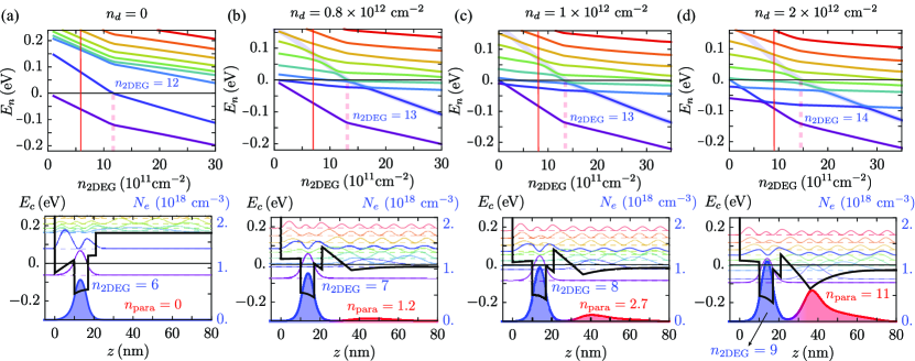
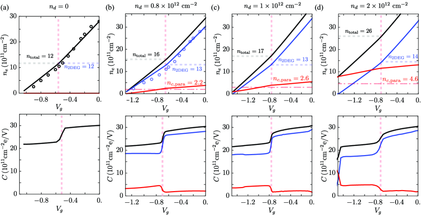
In this letter, we demonstrate a BSCR transition with profound consequences for the quality of shallow two-dimensional (2D) InAs QWs. This study is motivated by low-temperature transport measurements in state-of-the-art shallow InAs QWs reported in Ref. Zhang et al. (2023) [cf. Fig. 1 (d)], which serve as the fundamental building blocks for topological quantum computing hardware Aghaee et al. (2023, 2024). The energy levels and the electron populations of the QW bound states and the continuum can be continuously tunned by applying a gate voltage. At a low gate voltage, the potential well is shallow, with only the first subband occupied below the Fermi level () as a bound state inside the QW, while the excited resonances reside in the continuum. Increasing the gate voltage deepens the potential well, populating more 2D electron gas (2DEG) inside the QW. Consequently, the resonance second subband is gradually pulled down from the continuum, eventually becomes a bound state [cf. Fig.1 (a-c)]. If and when this second level is occupied, the mobility drops considerably because of the opening of an intersubband scattering channel. We calculate the electron density in the QW and in the parallel continuum channel as a function of the gate voltage, which shows a jump in capacitance at a 2DEG density corresponding to the occupation of the second subband (), in agreement with experiments Zhang et al. (2023) (cf. Fig. 2). We also predict the metal-insulator transition (MIT) in the parallel channel where bulk electrons near the Si doping layer breaks into puddles separated by random Coulomb disorder potential (cf. Table 1). An experimental puzzle in InAs QWs is the mobility drop at an electron density lower than expected for the bound-state second subband occupation. We explain this puzzle as a result of intersubband scattering between a bound state and a strongly level-broadened continuum resonance, mediated by screened Coulomb impurities [cf. Fig. 3 (a)]. This level broadening effect is directly related to hybridization with continuum and to the single-particle scattering time through the quantum uncertainty principle , which characterizes the disorder and reflects QW quality.
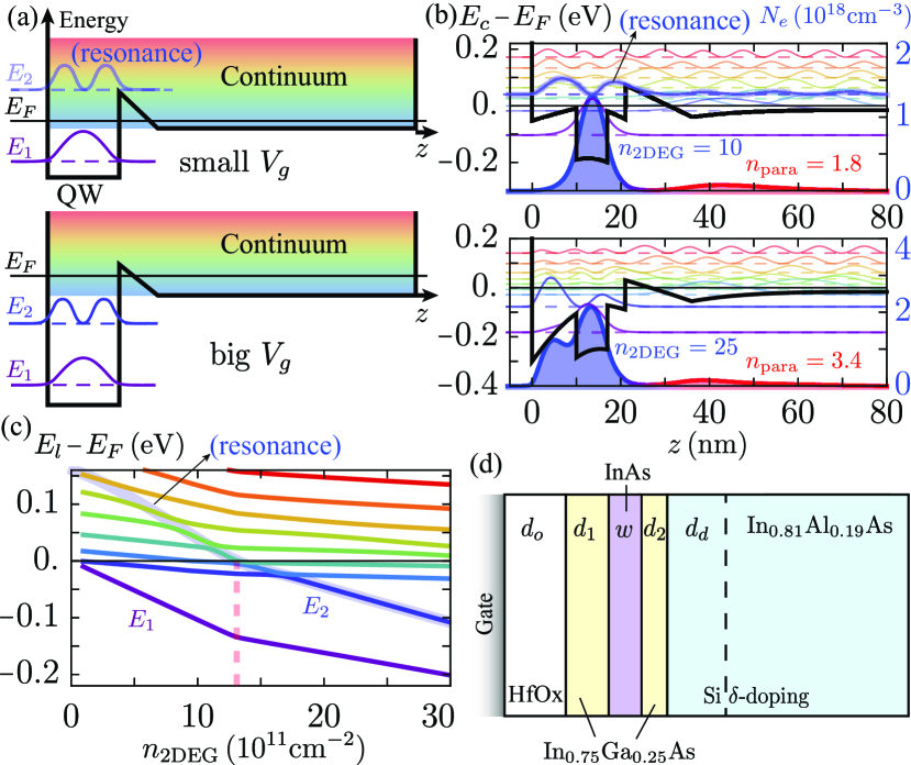
BSCR transition.—The energy levels and the electron density profile in a conduction band modified by the electrostatic potential are obtained by solving the self-consistent Hartree equation at sup . In our calculation, we use the same material parameters as the InAs sample reported in Ref. Zhang et al. (2023) [cf. Fig. 1 (d), where nm, nm, nm, nm, and nm]. (Because of the small InAs electron effective mass, exchange-correlation effects are negligible which we have explicitly checked by carrying out LDA calculations). In addition to a constant electric field contributed from the metallic gate, the positively charged donors in the modulation doped Si -layer of concentration cm-2 attract electrons and pull down the conduction band edge, while the repulsive self energy of electrons pushes up the conduction band edge. As a result, the QW splits into two conduction channels: the 2DEG channel of a concentration where electrons are localized inside the InAs QW, and the parallel continuum channel of a concentration where electrons are distributed in the bulk centered near the Si doping layer. Meanwhile, the applied gate voltage pumps electrons in/out the QW by shifting the semiconductor Fermi level relative to the Fermi level in the metallic gate . In the rest of this letter, we use to represent . Fig. 1 (c) shows the calculated eigenenergies relative to as a function of . We see that the second bound state , originally isolated from the continuum at high density, is pushed into the continuum and becomes a resonance by lowering . During this BSCR transition, the second subband occupation is marked by a red dashed line. Fig. 1 (b) shows the conduction band edge and the two-channel electron density profile (blue and red represent the 2DEG and parallel channel, respectively) corresponding to two different slices in Fig. 1 (c). We see that at small cm-2, only the first subband is occupied as a bound state, while the unoccupied second subband resides in the continuum as a resonance. The resonance tunnels through the Schottky barrier created by the Si donors with a finite probability, and hybridizes with the bulk continuum. The tunneling action is given by . For a tunneling barrier meV and tunneling length nm, we have , so that the probability density inside the QW is times larger than in the bulk. The smaller , the closer the resonance energy level to the top of the Schottky barrier with a smaller tunneling action, and the larger the hybridization with the continuum. This hybridization opens a gap in the subband spectrum that decreases as the density increases. On the other hand, at a high density cm-2, both the first and second subbands are occupied as bound states. The second subband wavefunction overflows from the InAs QW to the InGaAs regime with a barrier height meV, confined by the higher InAlAs barrier with meV.
Below we analytically prove that InAs QW at low density is so shallow that only the lowest subband is a bound state while all excited subbands are in the continuum. Since the wavefunction shape of the lowest subband does not change much by varying voltage at low density, we can use the finite potential well approximation to analytically compute the first subband energy by solving Davies (1997); Huang and Das Sarma (2024a). Here and is the first subband energy assuming an infinite potential well. For the InAs QW of interest, meV, much larger than the InGaAs barrier meV, which justifies the shallow QW picture. In the limit of , we find . Here and we obtain . Since must be satisfied for the second subband, all excited resonances are in the continuum.
| Sample | |||||||
| B | 8 | 7 | 0 | 1.2 | 2.2 | 0 | 1.8 |
| C | 10 | 8 | 2.3 | 2.7 | 2.6 | 4.8 | 3.1 |
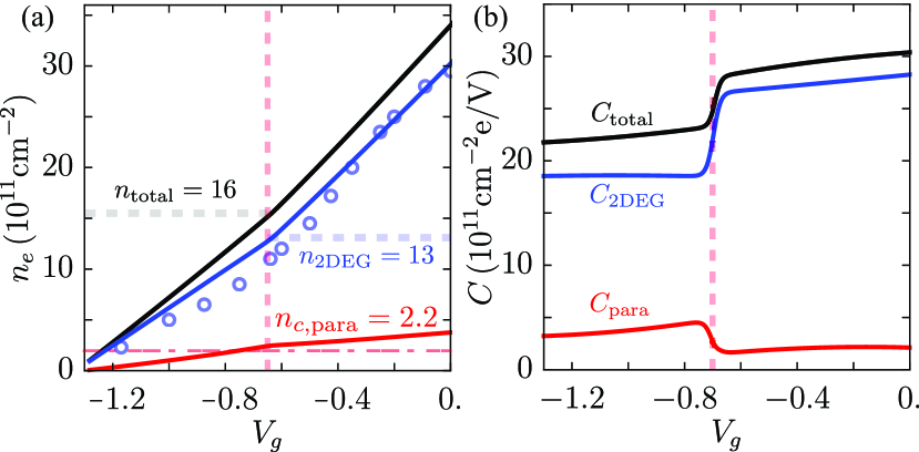
Capacitance jump and the parallel MIT.—The capacitance per unit area is defined as . In Fig. 2 (a), we compute the electron density versus voltage by identifying and fixing as the reference potential sup , in good agreement with the experimental data (blue circles). We see a capacitance jump at cm-2, corresponding to the second subband occupation. This capacitance jump can be understood by a simple electrostatic model consisting of two capacitors in series . Here and are the 2DEG geometric and quantum capacitance, respectively. is the dielectric constant in InAs, nm is the distance from the gate to the center of QW, , and is the density of states (DOS). Due to the second subband occupation, either as a bound state or as a continuum resonance, jumps by a factor of 2 and decreases from nm to nm, so that the effective capacitor thickness changes by a factor of . This explains that the 2DEG capacitance jumps up by a factor of . On the other hand, the parallel channel becomes less sensitive to since the gate electric field is more effectively screened by 2DEG electrons with higher DOS. Therefore, jumps down while jumps up.
We predict a MIT in the parallel channel near the capacitance jump [cf. Fig. 2 (a) and Table 1]. At small , electrons are localized and spatially separated as puddles in the parallel channel by random Coulomb disorder potential sup , where nm is the effective Bohr radius. When or , there is a MIT where electron puddles percolate through the disorder potential Last and Thouless (1971); Shklovskii and Efros (1972); Kirkpatrick (1973); Shklovskii and Efros (1975, 1984); Sarma and Hwang (2005); Shklovskii (2007); Adam et al. (2007); Manfra et al. (2007); Tracy et al. (2009); Das Sarma et al. (2005, 2013, 2014); Huang et al. (2021); Huang and Shklovskii (2021); Huang et al. (2022b, c). The parallel channel transitions from an insulator to a metal through the percolative 2D MIT when increases by increasing or . In Table 1, we estimate the metallic parallel mobility through sup ; Das Sarma and Hwang (2013); Huang and Das Sarma (2024a, b), in good agreement with experiments Zhang et al. (2023). Here and is the Thomas-Fermi screening wave vector.
Below we estimate the electron density at which second subband is occupied. The QW depth is modified by the electric field across a distance between the QW center and the oxide-semiconductor interface. According to quantum mechanics, the necessary condition for the existence of a second bound state inside QW is Davies (1997). Since is essentially pinned near the bottom of the continuum due to screening of the gate electric field by 2DEG, relative to the continuum subbands changes slowly when we change the electron density. Therefore, a simple estimation of the electron density when the second subband occupation is given by . Using cm-2, and nm, we obtain cm-2, in agreement with the result shown in Fig. 2. We also check the condition estimates the second subband occupation density reasonably well for other samples with different doping densities sup ; Zhang et al. (2023).
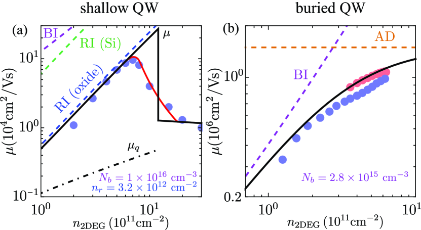
Mobility drop.—Before we discuss the mobility drop in a shallow InAs QW Zhang et al. (2023) at high 2DEG density, we discuss the low-density mobility behavior where only the first subband is occupied as a bound state to extract disorder information. Using Boltzmann transport theory Ando et al. (1982); Huang and Das Sarma (2024a), in Fig. 3 (a), we compute the mobility versus density with realistic disorder scattering modeled as follows. We model a -layer of charged impurities of 2D concentration located at the semiconductor-oxide interface at nm away from the center of the QW. Since , they scatter 2DEG as remote impurities (RIs) with a characteristic mobility density dependence Das Sarma and Hwang (2013). The other contribution to the RI scattering is from Si -layer with a doping density cm-2, located inside the bottom InAlAs barrier at nm. However, since the Si doping layer is further away from the center of the QW, the scattering from Si donors should contribute less than from the closer oxide RIs, as we confirm numerically in Fig. 3.
We model a uniform distribution of background charged impurities (BIs) with a 3D density . One can estimate from the mobility density data of buried InAs QWs reported in Ref. Hatke et al. (2017) [cf. Fig. 3 (b), “buried” means that InGaAs barriers with nm are much thicker than those in shallow QWs], where a high peak mobility exceeding cm2/Vs with and 0.5–1 Shabani et al. (2014); Dempsey et al. (2024) suggests that the mobility of buried InAs QWs is limited by unintentional BIs with cm-3, in good agreement with the estimation reported in Ref. Hatke et al. (2017). Since the screening parameter is much smaller than 1 in the experimental density range, the screening of BIs is rather weak, making them behave similar to RIs with a characteristic power law Das Sarma and Hwang (2013). On the other hand, in shallow InAs QWs reported in Ref. Zhang et al. (2023), the BI contribution to the mobility corresponding to cm-3 is much higher than the experimental mobility [cf. Fig. 3 (a)], which suggests that BI is not the limiting scattering source.
In Fig. 3, we show that alloy disorder (AD) scattering is negligible in shallow InAs QWs which corresponds to a rather high mobility cm2/Vs, while AD is one of the mobility limiting factors for buried InAs QWs. (In the calculation, we use the unscreened short-range AD potential eV Bastard (1983); Gold (1988); Dong et al. (2024)). Since the interfaces between InAs QW and InGaAs barriers should be of similar quality in Refs. Zhang et al. (2023) and Hatke et al. (2017), and since the interface roughness (IR) scattering predicts a mobility proportional to Gold (1988); Ando et al. (1982), the fact that the narrower nm buried QW Hatke et al. (2017) has a much higher mobility than the wider nm shallow QW Zhang et al. (2023) indicates that IR is not the limiting scattering mechanism in the wider QW (IR scattering is weaker for a wider QW). The low-density quantum mobility is shown as a dot-dashed black curve in Fig. 3 (a). is much smaller than since small-angle forward scattering from distant charged impurity is included in but not in Das Sarma and Stern (1985); Sammon et al. (2018).
Next, we discuss the mobility drop at high density, which is a persistent prominent feature in shallow InAs QWs Zhang et al. (2023). Experimentally, mobility reaches the maximum cm2/Vs at cm-2 [cf. Fig. 3 (a)]. Such electron density is substantially smaller than expected for the second subband occupation cm-2 estimated from the capacitance jump (cf. Fig. 2), and from the Landau level (LL) crossing seen in magnetotransport Zhang et al. (2023). This is a serious conundrum. We have two main reasons to believe that the best explanation for such a mobility drop is intersubband scattering between the bound-state first subband and the strongly level-broadened second subband as a continuum resonance, mediated by Coulomb impurities. In other words, the level-broadened resonance effectively acts as a continumm with a continuous DOS tail that smears the mobility drop. First, since the mobility continuously and smoothly drops for the whole higher density range, without showing other features, the only dominant scattering mechanism at high density should be intersubband scattering. Otherwise, we should have seen an additional sharp decrease in mobility when the second subband is occupied at cm-2, which is absent in the data. Second, although short-range AD or IR usually affects high-density mobility stronger since the long-range charged impurities are screened Das Sarma and Hwang (2013, 2014), we argue that AD and IR are negligible even if the second subband is occupied, and the dominant scattering source are charged impurities. This is because the second subband wavefunction, residing in the InGaAs barrier, on average is much closer to the oxide and Si charged impurities compared to the first subband. Consequently, Coulomb scattering is strongly enhanced and overwhelms other scattering sources. For example, AD scattering rate is proportional to the squared probability leaking in the alloy region Bastard (1983); Gold (1988); Dong et al. (2024). The leakage probability is % for the first subband and % for the second subband, leading to a decrease in mobility cm2/Vs. However, such mobility is still much larger than the experimental mobility so AD is negligible. IR scattering should not limits the second subband mobility either due to a larger effective well width , contributing to a scattering rate Gold (1988); Ando et al. (1982) even weaker than in first subband.
If there is no level broadening, there should be a sharp mobility decrease when the second subband is occupied Mori and Ando (1979); Störmer et al. (1982); Das Sarma and Xie (1987); Fletcher et al. (1988); Ensslin et al. (1993); Muraki et al. (2001) [cf. the solid black curve in Fig. 3 (a)]. We approximate the multisubband 2DEG as a 3DEG distributed over a thickness of to estimate the high-density mobility, dominated by intersubband scattering mediated by Coulomb impurities, through the Brooks-Herring formula Brooks (1951, 1955); Chattopadhyay and Queisser (1981); bro , where . As a result, the mobility at high density is cm2/Vs, in reasonable agreement with experiments Zhang et al. (2023). However, the theory without level broadening predicts a sharper mobility drop at a larger density cm-2 compared to the smoother drop at cm-2 in experiments. This discrepancy cm-2 can be explained by a resonance strongly level-broadened via disorder and hybirdization with the continuum, so that the second subband resonance is smeared in an energy window of meV. The mobility including the level broadening effect by smearing the scattering rate in an energy window of is shown as the red curve in Fig. 3 (a) cou . Because of the long-range Coulomb potential fluctuation meV, the second subband becomes an impurity band whose bottom is brought down by an amount of . This is consistent with the broadening of LL crossings observed through magnetotransport Zhang et al. (2023), where an energy-resolved LL crossing first shows up at T corresponding to a cyclotron energy meV and to the second-subband quantum mobility cm2/Vs. This is comparable to the low-density first-subband shown as a dot-dashed line in Fig. 2 (a). Similar results of meV have been measured from Dingle temperature of Shubnikov-de Haas oscillations in narrower InAs QWs Yuan et al. (2020). In addition, the hybridization between a resonance and the continuum also contributes to the level broadening. The physics is that electrons can be scattered to subbands close to the resonance as long as their wavefunctions sufficiently localized inside QW that resemble excited “bound states”. At cm-2, the hybridization gap is meV [cf. Fig. 1 (c)], comparable to induced by disorder. The difference between the density corresponding to the capacitance jump and to the onset of mobility drop may be explained by a mobility edge near the level-broadened second subband bottom (). Namely, the additional channel for scattering from the first to the second subband influences the mobility even though there are no mobile carriers in the second subband Fletcher et al. (1988). Similar level broadening effect has been discussed in GaAs Störmer et al. (1982); Fletcher et al. (1988); Ensslin et al. (1993); Muraki et al. (2001), but with a much smaller meV corresponding to a much higher cm2/Vs.
Conclusions.—We have shown a transition from a bound state to a continuum resonance in a shallow quantum well, strongly tunnable by electrostatic gating. Using intersubband scattering involving a strongly level-broadened continuum resonance mediated by Coulomb impurities, we have explained the experimental puzzle in shallow InAs quantum wells that the mobility drops at an electron density smaller than expected for the bound-state second subband occupation. Moreover, we have explained the experimentally observed capacitance jump and the metal-insulator transition in the parallel continuum channel accompanied the bound state-continuum resonance transition. Our findings provide guidelines for enhancing the electrostatic control and sample quality of shallow InAs quantum wells, allowing further exploration and sample improvement of solid-state-based topological quantum computing platforms, which is currently the key stumbling block inhibiting the manifestation of non-Abelian Majorana zero modes.
We acknowledge helpful conversation with Alisa Danilenko. This work is supported by the Laboratory for Physical Sciences.
References
- Ando et al. (1982) T. Ando, A. B. Fowler, and F. Stern, Electronic properties of two-dimensional systems, Rev. Mod. Phys. 54, 437 (1982).
- Zhang et al. (2023) T. Zhang, T. Lindemann, G. C. Gardner, S. Gronin, T. Wu, and M. J. Manfra, Mobility exceeding 100 000 s in modulation-doped shallow InAs quantum wells coupled to epitaxial aluminum, Phys. Rev. Mater. 7, 056201 (2023).
- Chung et al. (2021) Y. J. Chung, K. A. Villegas Rosales, K. W. Baldwin, P. T. Madathil, K. W. West, M. Shayegan, and L. N. Pfeiffer, Ultra-high-quality two-dimensional electron systems, Nature Materials 20, 632 (2021).
- Ahn and Das Sarma (2022) S. Ahn and S. Das Sarma, Density-dependent two-dimensional optimal mobility in ultra-high-quality semiconductor quantum wells, Phys. Rev. Mater. 6, 014603 (2022).
- Huang et al. (2022a) Y. Huang, B. I. Shklovskii, and M. A. Zudov, Scattering mechanisms in state-of-the-art GaAs/AlGaAs quantum wells, Phys. Rev. Mater. 6, L061001 (2022a).
- Esposti et al. (2023) D. D. Esposti, L. E. A. Stehouwer, Önder Gül, N. Samkharadze, C. Déprez, M. Meyer, I. N. Meijer, L. Tryputen, S. Karwal, M. Botifoll, J. Arbiol, S. V. Amitonov, L. M. K. Vandersypen, A. Sammak, M. Veldhorst, and G. Scappucci, Low disorder and high valley splitting in silicon, arXiv:2309.02832 [cond-mat.mes-hall] (2023).
- Huang and Das Sarma (2024a) Y. Huang and S. Das Sarma, Understanding disorder in silicon quantum computing platforms: Scattering mechanisms in Si/SiGe quantum wells, Phys. Rev. B 109, 125405 (2024a).
- Aghaee et al. (2023) M. Aghaee, A. Akkala, Z. Alam, R. Ali, A. Alcaraz Ramirez, M. Andrzejczuk, A. E. Antipov, P. Aseev, M. Astafev, B. Bauer, J. Becker, S. Boddapati, F. Boekhout, J. Bommer, T. Bosma, L. Bourdet, S. Boutin, P. Caroff, L. Casparis, M. Cassidy, S. Chatoor, A. W. Christensen, N. Clay, W. S. Cole, F. Corsetti, A. Cui, P. Dalampiras, A. Dokania, G. de Lange, M. de Moor, J. C. Estrada Saldaña, S. Fallahi, Z. H. Fathabad, J. Gamble, G. Gardner, D. Govender, F. Griggio, R. Grigoryan, S. Gronin, J. Gukelberger, E. B. Hansen, S. Heedt, J. Herranz Zamorano, S. Ho, U. L. Holgaard, H. Ingerslev, L. Johansson, J. Jones, R. Kallaher, F. Karimi, T. Karzig, E. King, M. E. Kloster, C. Knapp, D. Kocon, J. Koski, P. Kostamo, P. Krogstrup, M. Kumar, T. Laeven, T. Larsen, K. Li, T. Lindemann, J. Love, R. Lutchyn, M. H. Madsen, M. Manfra, S. Markussen, E. Martinez, R. McNeil, E. Memisevic, T. Morgan, A. Mullally, C. Nayak, J. Nielsen, W. H. P. Nielsen, B. Nijholt, A. Nurmohamed, E. O’Farrell, K. Otani, S. Pauka, K. Petersson, L. Petit, D. I. Pikulin, F. Preiss, M. Quintero-Perez, M. Rajpalke, K. Rasmussen, D. Razmadze, O. Reentila, D. Reilly, R. Rouse, I. Sadovskyy, L. Sainiemi, S. Schreppler, V. Sidorkin, A. Singh, S. Singh, S. Sinha, P. Sohr, T. c. v. Stankevič, L. Stek, H. Suominen, J. Suter, V. Svidenko, S. Teicher, M. Temuerhan, N. Thiyagarajah, R. Tholapi, M. Thomas, E. Toomey, S. Upadhyay, I. Urban, S. Vaitiekėnas, K. Van Hoogdalem, D. Van Woerkom, D. V. Viazmitinov, D. Vogel, S. Waddy, J. Watson, J. Weston, G. W. Winkler, C. K. Yang, S. Yau, D. Yi, E. Yucelen, A. Webster, R. Zeisel, and R. Zhao (Microsoft Quantum), InAs-Al hybrid devices passing the topological gap protocol, Phys. Rev. B 107, 245423 (2023).
- Aghaee et al. (2024) M. Aghaee, A. A. Ramirez, Z. Alam, R. Ali, M. Andrzejczuk, A. Antipov, M. Astafev, A. Barzegar, B. Bauer, J. Becker, U. K. Bhaskar, A. Bocharov, S. Boddapati, D. Bohn, J. Bommer, L. Bourdet, A. Bousquet, S. Boutin, L. Casparis, B. J. Chapman, S. Chatoor, A. W. Christensen, C. Chua, P. Codd, W. Cole, P. Cooper, F. Corsetti, A. Cui, P. Dalpasso, J. P. Dehollain, G. de Lange, M. de Moor, A. Ekefjärd, T. E. Dandachi, J. C. E. Saldaña, S. Fallahi, L. Galletti, G. Gardner, D. Govender, F. Griggio, R. Grigoryan, S. Grijalva, S. Gronin, J. Gukelberger, M. Hamdast, F. Hamze, E. B. Hansen, S. Heedt, Z. Heidarnia, J. H. Zamorano, S. Ho, L. Holgaard, J. Hornibrook, J. Indrapiromkul, H. Ingerslev, L. Ivancevic, T. Jensen, J. Jhoja, J. Jones, K. V. Kalashnikov, R. Kallaher, R. Kalra, F. Karimi, T. Karzig, E. King, M. E. Kloster, C. Knapp, D. Kocon, J. Koski, P. Kostamo, M. Kumar, T. Laeven, T. Larsen, J. Lee, K. Lee, G. Leum, K. Li, T. Lindemann, M. Looij, J. Love, M. Lucas, R. Lutchyn, M. H. Madsen, N. Madulid, A. Malmros, M. Manfra, D. Mantri, S. B. Markussen, E. Martinez, M. Mattila, R. McNeil, A. B. Mei, R. V. Mishmash, G. Mohandas, C. Mollgaard, T. Morgan, G. Moussa, C. Nayak, J. H. Nielsen, J. M. Nielsen, W. H. P. Nielsen, B. Nijholt, M. Nystrom, E. O’Farrell, T. Ohki, K. Otani, B. P. Wütz, S. Pauka, K. Petersson, L. Petit, D. Pikulin, G. Prawiroatmodjo, F. Preiss, E. P. Morejon, M. Rajpalke, C. Ranta, K. Rasmussen, D. Razmadze, O. Reentila, D. J. Reilly, Y. Ren, K. Reneris, R. Rouse, I. Sadovskyy, L. Sainiemi, I. Sanlorenzo, E. Schmidgall, C. Sfiligoj, M. B. Shah, K. Simoes, S. Singh, S. Sinha, T. Soerensen, P. Sohr, T. Stankevic, L. Stek, E. Stuppard, H. Suominen, J. Suter, S. Teicher, N. Thiyagarajah, R. Tholapi, M. Thomas, E. Toomey, J. Tracy, M. Turley, S. Upadhyay, I. Urban, K. V. Hoogdalem, D. J. V. Woerkom, D. V. Viazmitinov, D. Vogel, J. Watson, A. Webster, J. Weston, G. W. Winkler, D. Xu, C. K. Yang, E. Yucelen, R. Zeisel, G. Zheng, and J. Zilke, Interferometric single-shot parity measurement in an InAs-Al hybrid device, arXiv:2401.09549 [cond-mat.mes-hall] (2024).
- Dartiailh et al. (2021a) M. C. Dartiailh, J. J. Cuozzo, B. H. Elfeky, W. Mayer, J. Yuan, K. S. Wickramasinghe, E. Rossi, and J. Shabani, Missing Shapiro steps in topologically trivial Josephson junction on InAs quantum well, Nature Communications 12, 78 (2021a).
- Dartiailh et al. (2021b) M. C. Dartiailh, W. Mayer, J. Yuan, K. S. Wickramasinghe, A. Matos-Abiague, I. Žutić, and J. Shabani, Phase signature of topological transition in Josephson junctions, Phys. Rev. Lett. 126, 036802 (2021b).
- Banerjee et al. (2023) A. Banerjee, O. Lesser, M. A. Rahman, H.-R. Wang, M.-R. Li, A. Kringhøj, A. M. Whiticar, A. C. C. Drachmann, C. Thomas, T. Wang, M. J. Manfra, E. Berg, Y. Oreg, A. Stern, and C. M. Marcus, Signatures of a topological phase transition in a planar Josephson junction, Phys. Rev. B 107, 245304 (2023).
- Ahn et al. (2021) S. Ahn, H. Pan, B. Woods, T. D. Stanescu, and S. Das Sarma, Estimating disorder and its adverse effects in semiconductor Majorana nanowires, Phys. Rev. Mater. 5, 124602 (2021).
- Das Sarma et al. (2023) S. Das Sarma, J. D. Sau, and T. D. Stanescu, Spectral properties, topological patches, and effective phase diagrams of finite disordered Majorana nanowires, Phys. Rev. B 108, 085416 (2023).
- Das Sarma and Pan (2023) S. Das Sarma and H. Pan, Density of states, transport, and topology in disordered Majorana nanowires, Phys. Rev. B 108, 085415 (2023).
- Das Sarma (2023) S. Das Sarma, In search of Majorana, Nature Physics 19, 165 (2023).
- (17) See Supplemental Material at [url] for the algorithm to solve the self-consistent Hartree equation and more detailed discussion of metal-insulator transition.
- Davies (1997) J. H. Davies, The Physics of Low-dimensional Semiconductors: An Introduction (Cambridge University Press, 1997) pp. 118–149, 318–321.
- Last and Thouless (1971) B. J. Last and D. J. Thouless, Percolation theory and electrical conductivity, Phys. Rev. Lett. 27, 1719 (1971).
- Shklovskii and Efros (1972) B. I. Shklovskii and A. L. Efros, Completely compensated crystalline semiconductor as a model of an amorphous semi- conductor, Zh. Eksp. Teor. Fiz. 62, 1156 (1972), [Sov. Phys. - JETP 35, 610 (1972)].
- Kirkpatrick (1973) S. Kirkpatrick, Percolation and conduction, Rev. Mod. Phys. 45, 574 (1973).
- Shklovskii and Efros (1975) B. I. Shklovskii and A. L. Efros, Percolation theory and conductivity of strongly inhomogeneous media, Soviet Physics Uspekhi 18, 845 (1975).
- Shklovskii and Efros (1984) B. I. Shklovskii and A. L. Efros, Electronic Properties of Doped Semiconductors (Springer, Berlin, 1984).
- Sarma and Hwang (2005) S. D. Sarma and E. Hwang, The so-called two dimensional metal–insulator transition, Solid State Communications 135, 579 (2005).
- Shklovskii (2007) B. I. Shklovskii, Simple model of coulomb disorder and screening in graphene, Phys. Rev. B 76, 233411 (2007).
- Adam et al. (2007) S. Adam, E. H. Hwang, V. M. Galitski, and S. D. Sarma, A self-consistent theory for graphene transport, Proceedings of the National Academy of Sciences 104, 18392 (2007).
- Manfra et al. (2007) M. J. Manfra, E. H. Hwang, S. Das Sarma, L. N. Pfeiffer, K. W. West, and A. M. Sergent, Transport and percolation in a low-density high-mobility two-dimensional hole system, Phys. Rev. Lett. 99, 236402 (2007).
- Tracy et al. (2009) L. A. Tracy, E. H. Hwang, K. Eng, G. A. Ten Eyck, E. P. Nordberg, K. Childs, M. S. Carroll, M. P. Lilly, and S. Das Sarma, Observation of percolation-induced two-dimensional metal-insulator transition in a si mosfet, Phys. Rev. B 79, 235307 (2009).
- Das Sarma et al. (2005) S. Das Sarma, M. P. Lilly, E. H. Hwang, L. N. Pfeiffer, K. W. West, and J. L. Reno, Two-dimensional metal-insulator transition as a percolation transition in a high-mobility electron system, Phys. Rev. Lett. 94, 136401 (2005).
- Das Sarma et al. (2013) S. Das Sarma, E. H. Hwang, and Q. Li, Two-dimensional metal-insulator transition as a potential fluctuation driven semiclassical transport phenomenon, Phys. Rev. B 88, 155310 (2013).
- Das Sarma et al. (2014) S. Das Sarma, E. H. Hwang, K. Kechedzhi, and L. A. Tracy, Signatures of localization in the effective metallic regime of high-mobility Si MOSFETs, Phys. Rev. B 90, 125410 (2014).
- Huang et al. (2021) Y. Huang, Y. Ayino, and B. I. Shklovskii, Metal-insulator transition in -type bulk crystals and films of strongly compensated , Phys. Rev. Mater. 5, 044606 (2021).
- Huang and Shklovskii (2021) Y. Huang and B. I. Shklovskii, Disorder effects in topological insulator thin films, Phys. Rev. B 103, 165409 (2021).
- Huang et al. (2022b) Y. Huang, Y. He, B. Skinner, and B. I. Shklovskii, Conductivity of two-dimensional narrow gap semiconductors subjected to strong Coulomb disorder, Phys. Rev. B 105, 054206 (2022b).
- Huang et al. (2022c) Y. Huang, B. Skinner, and B. I. Shklovskii, Conductivity of two-dimensional small gap semiconductors and topological insulators in strong Coulomb disorder, Journal of Experimental and Theoretical Physics 135, 409 (2022c).
- Das Sarma and Hwang (2013) S. Das Sarma and E. H. Hwang, Universal density scaling of disorder-limited low-temperature conductivity in high-mobility two-dimensional systems, Phys. Rev. B 88, 035439 (2013).
- Huang and Das Sarma (2024b) Y. Huang and S. Das Sarma, Electronic transport, metal-insulator transition, and wigner crystallization in transition metal dichalcogenide monolayers, Phys. Rev. B 109, 245431 (2024b).
- Hatke et al. (2017) A. T. Hatke, T. Wang, C. Thomas, G. C. Gardner, and M. J. Manfra, Mobility in excess of cm2/Vs in InAs quantum wells grown on lattice mismatched InP substrates, Applied Physics Letters 111, 142106 (2017).
- Shabani et al. (2014) J. Shabani, S. Das Sarma, and C. J. Palmstrøm, An apparent metal-insulator transition in high-mobility two-dimensional InAs heterostructures, Phys. Rev. B 90, 161303 (2014).
- Dempsey et al. (2024) C. P. Dempsey, J. T. Dong, I. V. Rodriguez, Y. Gul, S. Chatterjee, M. Pendharkar, S. N. Holmes, M. Pepper, and C. J. Palmstrøm, Effects of strain compensation on electron mobilities in inas quantum wells grown on inp(001), arXiv:2406.19469 [cond-mat.mes-hall] (2024).
- Bastard (1983) G. Bastard, Energy levels and alloy scattering in InP‐In (Ga)As heterojunctions, Applied Physics Letters 43, 591 (1983).
- Gold (1988) A. Gold, Scattering time and single-particle relaxation time in a disordered two-dimensional electron gas, Phys. Rev. B 38, 10798 (1988).
- Dong et al. (2024) J. T. Dong, Y. Gul, A. N. Engel, T. A. J. van Schijndel, C. P. Dempsey, M. Pepper, and C. J. Palmstrøm, Enhanced mobility of ternary InGaAs quantum wells through digital alloying, arXiv:2403.17166 [cond-mat.mes-hall] (2024).
- Das Sarma and Stern (1985) S. Das Sarma and F. Stern, Single-particle relaxation time versus scattering time in an impure electron gas, Phys. Rev. B 32, 8442 (1985).
- Sammon et al. (2018) M. Sammon, M. A. Zudov, and B. I. Shklovskii, Mobility and quantum mobility of modern GaAs/AlGaAs heterostructures, Phys. Rev. Mater. 2, 064604 (2018).
- Das Sarma and Hwang (2014) S. Das Sarma and E. H. Hwang, Short-range disorder effects on electronic transport in two-dimensional semiconductor structures, Phys. Rev. B 89, 121413 (2014).
- Mori and Ando (1979) S. Mori and T. Ando, Intersubband scattering effect on the mobility of a Si (100) inversion layer at low temperatures, Phys. Rev. B 19, 6433 (1979).
- Störmer et al. (1982) H. Störmer, A. Gossard, and W. Wiegmann, Observation of intersubband scattering in a 2-dimensional electron system, Solid State Communications 41, 707 (1982).
- Das Sarma and Xie (1987) S. Das Sarma and X. C. Xie, Calculated transport properties of ultrasubmicrometer quasi-one-dimensional inversion lines, Phys. Rev. B 35, 9875 (1987).
- Fletcher et al. (1988) R. Fletcher, E. Zaremba, M. D’Iorio, C. T. Foxon, and J. J. Harris, Evidence of a mobility edge in the second subband of an Al0.33Ga0.67As-GaAs heterojunction, Phys. Rev. B 38, 7866 (1988).
- Ensslin et al. (1993) K. Ensslin, A. Wixforth, M. Sundaram, P. F. Hopkins, J. H. English, and A. C. Gossard, Single-particle subband spectroscopy in a parabolic quantum well via transport experiments, Phys. Rev. B 47, 1366 (1993).
- Muraki et al. (2001) K. Muraki, T. Saku, and Y. Hirayama, Charge excitations in easy-axis and easy-plane quantum Hall ferromagnets, Phys. Rev. Lett. 87, 196801 (2001).
- Brooks (1951) H. Brooks, in Proceedings of the American Physical Society, Vol. 83 (American Physical Society, 1951) p. 879.
- Brooks (1955) H. Brooks, in Advances in Electronics and Electron Physics, Vol. 7, edited by L. Marton (Academic, New York, 1955) p. 85.
- Chattopadhyay and Queisser (1981) D. Chattopadhyay and H. J. Queisser, Electron scattering by ionized impurities in semiconductors, Rev. Mod. Phys. 53, 745 (1981).
- (56) Although the charge compensation is unknown experimentally, we estimate the ratio of free carriers to Coulomb impurities as at cm-2 in the Brooks-Herring formula.
- (57) The full mobility at high density including the intersubband scattering and the level broadening effect can be numerically calculated using the coupled Boltzmann equation with a self-consistent Born approximation combined with the self-consistent wavefunctions and energy levels Mori and Ando (1979). Such numerical calculation containing two hierarchies of self-consistency is beyond the scope of this letter.
- Yuan et al. (2020) J. Yuan, M. Hatefipour, B. A. Magill, W. Mayer, M. C. Dartiailh, K. Sardashti, K. S. Wickramasinghe, G. A. Khodaparast, Y. H. Matsuda, Y. Kohama, Z. Yang, S. Thapa, C. J. Stanton, and J. Shabani, Experimental measurements of effective mass in near-surface InAs quantum wells, Phys. Rev. B 101, 205310 (2020).
- Stern and Das Sarma (1984) F. Stern and S. Das Sarma, Electron energy levels in GaAs-Ga1-xAlxAs heterojunctions, Phys. Rev. B 30, 840 (1984).
- Wickramasinghe et al. (2018) K. S. Wickramasinghe, W. Mayer, J. Yuan, T. Nguyen, L. Jiao, V. Manucharyan, and J. Shabani, Transport properties of near surface InAs two-dimensional heterostructures, Applied Physics Letters 113, 262104 (2018).
- Anderson (1958) P. W. Anderson, Absence of diffusion in certain random lattices, Phys. Rev. 109, 1492 (1958).
- Ioffe and Regel (1960) A. F. Ioffe and A. R. Regel, in Progress in Semiconductors, Vol. 4, edited by A. F. Gibson (Wiley, New York, 1960) pp. 237–291.
- Efros (1988) A. Efros, Non-linear screening and the background density of 2DEG states in magnetic field, Solid State Communications 67, 1019 (1988).
- Efros et al. (1993) A. L. Efros, F. G. Pikus, and V. G. Burnett, Density of states of a two-dimensional electron gas in a long-range random potential, Phys. Rev. B 47, 2233 (1993).
Supplementary materials
.1 Self-consistent Hartree equation
We discuss the algorithm we used to solve the self-consistent Hartree equation within the effective mass approximation at zero temperature Stern and Das Sarma (1984). The 1D Poisson’s equation for the electric potential reads
| (S1) |
where with , , and the positions of the Si -doping layer, of the unintentional total charge in the oxide-semiconductor interface, and of the gate, respectively, while , , and are the corresponding 2D charge densities. The charge neutrality condition ensures , where is the total electron density. is the dielectric constant as a function of the position along , which is material dependent. The boundary conditions (the reference potential and the boundary electric field) for the Poisson equation Eq. (S1) are
| (S2) |
where is the dielectric constant of the gate dielectrics. is the 3D electron density given by
| (S3) | |||
| (S4) |
where is the electron density for the -th subband, is the density of states (DOS) for a subband with the DOS effective mass of the 2DEG with a parabolic dispersion [c.f. Eq. (S6) below]. and are the corresponding subband eigenenergy and wavefunction for the 1D Schrödinger’s equation along -direction
| (S5) |
with a boundary condition . is the conduction band bottom profile. In deriving Eq. (S5), we assume and are independent on , so that the full Schrödinger’s equation can be separated into two equations. The first is Eq. (S5) which depends only on , and the second is for the plane wave with a dispersion
| (S6) |
and the total energy is . The electric potential enters Schrödinger’ equation as a Hartree energy, which in turn determines the eigenenergy and the electron density that generate the electrostatic potential through Eqs. (S3) and (S4). In other words, the electron density is a functional of the electric potential , which makes the Poisson equation nonlinear. As a result, Poisson’s equation (S1) and Schrödinger’s equation (S5) should be solved together self-consistently.
The self-consistent algorithm to solve Eqs. (S1) and (S5) is as follows. The initial state for the electron density we choose for the iterative algorithm is that generates the initial electric potential according to the Poisson equation
| (S7) |
Given an initial , our goal is to find the exact solution to Poisson’s equation, denoted . (We have checked that the convergent result of after the iterative algorithm is robust in different initial conditions since the electrostatic solution is unique). We achieve this goal by iteratively updating the electric potential, so that the sequence converges to in the sense that for all positions . As the first step in the iteration, to obtain from , we substitute for in Schrödinger’s equation Eq. (S5) and obtain the corresponding electron density through Eqs. (S3) and (S4). We then substitute into Eq. (S1) as a source term, and we solve it for . In general, depends on through
| (S8) |
To ensure convergence of the iteration algorithm, we mix the electron density of the previous two adjacent steps before we substitute it into Poisson’s equation to obtain the electric potential of the current step, so that if we choose a small . In other words, instead of Eq. (S8), we solve the following equation
| (S9) |
We stop the iteration process at some finite once for all positions with a small cutoff , and the algorithm is numerically converged.
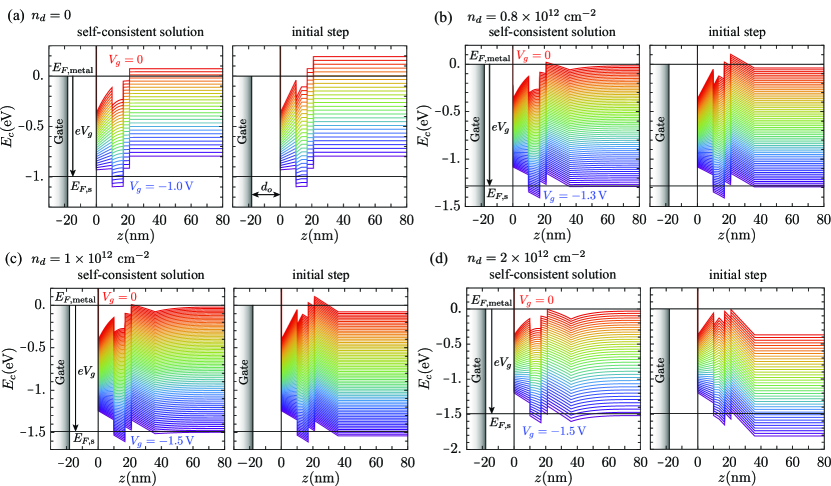
To model the conduction band bottom profile for the device structures in Ref. Zhang et al. (2023) [c.f. Fig. 1 (d) in the main text], we use the conduction band bottom difference meV between InAs and In0.75Ga0.25As, and meV between InAs and In0.81Al0.19As. The difference in the work function between HfOx and In0.75Ga0.25As contributes to a high barrier eV at the oxide-semiconductor interface. We assume that there is a high barrier between the buffer layers and In0.81Al0.19As barrier, so that the wavefunction vanishes at this boundary (we check that by lowering this barrier height, only the level spacing within the continuum states changes to a smaller value, which enhances the physics of the continuum described in the main text). Since the effective masses in the In0.75Ga0.25As and In0.81Al0.19As barriers are not very different from the effective mass in InAs Wickramasinghe et al. (2018), we use a uniform isotropic effective mass for the whole structure. We choose a uniform dielectric constant , since in HfOx is close to in semiconductor . The results of the conduction band bottom profile at different gate voltages for samples of different doping are shown in Fig. S1. The corresponding subband energies relative to as functions of are shown in Fig. S2 first row.
As explained in the main text, the gate electric field changes the electrostatic potential profile dramatically such that the portions of electron density populating the 2DEG and the parallel channels, and , are changed by the gate voltage. Meanwhile, the gate voltage tune the total electron density by changing the position of the semiconductor Fermi level in the QW relative to the metal Fermi level in the gate (cf. Fig. S1). As a result, and are functions of the total electron density . A straight forward way to obtain the 2DEG density and the parasitic density from the 3D electron density is to first divide into two parts by finding the minimum where , so that
| (S10) |
Another way to compute and is as follows. We first find the dispersion of the subband energy as a function of the total electron density , and then identify the subbands that belong to the 2DEG channel by tracing the level crossings and doing the interpolation in , such that is given by
| (S11) |
and . We check that these two methods give essentially identical results of and , while the first method gives a slightly smoother dependence on because the second method requires a numerical interpolation, so we choose the first method to present our results.
Figure S2 second row shows the electron density profile (shaded color regime) and the conduction band edge (thick black curve) corresponding to a specific at (cf. the red vertical line in Fig. S2 first row). We see that by increasing the doping density , the electron density in the parallel channel increases dramatically while the increase in the electron density in the 2DEG channel is mediocre. The thin solid (dashed) colored lines represent the wavefunction (eigenenergies). For Sample A which is undoped, the second subband (thin blue) is a bound state overflowing to the InGaAs barrier regime, confined by the higher InAlAs barrier. For Sample B-D which is modulation doped, the second subband in the 2DEG channel becomes an excited resonance hybridized with the continuum.
From Fig. 2 (a) reported in Ref. Zhang et al. (2023), we notice that samples with different dopings all decay to the same mobility at high electron density, while the electron density at increases as the doping density goes up [cf. Fig. S2 second row]. The low-density mobility behavior are essentially the same for all samples of different doping. This indicates that the scattering source responsible for the transport mobility are similar for different samples while the level broadening are different for different samples due to the difference in the single-particle (quantum) scattering rate . Since the quantum mobility is affected by more distant Coulomb impurities which provide small-angle scattering while the transport mobility is more sensitive to the closer charged impurities that provide back scattering Das Sarma and Stern (1985); Sammon et al. (2018), this implies that the scattering amplitude of distant Coulomb impurities are different for different doping samples. Indeed, for the undoped Sample A, there is no excess electrons in the bulk parallel channel to screen the distant charges, which decreases the quantum mobility and increases the level broadening. For the doped Samples B-D, the excess electrons screen the distant charges more effectively and decreases the level broadening, which shifts the peak position closer to the second subband occupation.
To compute the capacitance numerically, we assume the gate is a perfect metal with an infinite DOS, so that is not changed by applying gate voltage. We can use as a reference zero potential in the calculation of by setting . Using the relationship , the differential capacitance per unit area is given by . The results are shown in Fig. S3.
.2 Metal-insulator transition
Below we show that at the 2DEG density corresponding to for samples of different Si doping densities in Ref. Zhang et al. (2023), the parallel channels in Sample B have electron density smaller than the MIT critical density so they are localized and do not contribute to transport, while the parallel channels in Samples C and D have electron density larger than the MIT critical density so they are conducting, in agreement with Hall measurements in Ref. Zhang et al. (2023).
The mean-squared fluctuation of potential energy generated by random Coulomb impurities in a 2D plane reads
| (S12) |
Eq. (S12) is valid if the number of charged impurities inside the non-linear screening radius (which we justify below), and the charge number fluctuation is . One can obtain the same result of mean-squared potential fluctuation in Eq. (S12) by calculating the on-site potential correlator in the Fourier space
| (S13) |
where is the ultraviolet cutoff and is the screening wavevector. Here is the total Coulomb potential summing all the impurities, is the Coulomb potential for a single Coulomb impurity located at , is the total area of the system, and averages over all the random realizations of impurities position.
When the kinetic energy of the parallel channel is smaller than the potential energy fluctuation , the electron density in the parasitic channel screens the charge fluctuation such that . At the transition, the kinetic energy of electrons should be equal to the potential fluctuation so that electrons overcome the random potential barriers to percolate through the system and become delocalized Shklovskii and Efros (1984). Solving together with , we obtain
| (S14) | |||
| (S15) |
Using Eqs. (S14) and (S15), the theoretically predicted and for Samples B, C, and D with different Si doping densities are summarized in Table S1. We find cm-2 and nm, which justifies the assumption that . We mark these values of as red dot-dashed horizontal lines in the middle row of Figs. S3 (b-d). By comparing the predicted critical density with the carrier density in the parallel channel, we find the parallel channel in Sample B is insulating where , while for Sample C and D the parallel channel is already metallic . We also estimate the mobility in the parallel channel through Das Sarma and Hwang (2013); Huang and Das Sarma (2024a, b)
| (S16) |
where , which is good for in-plane charged impurity scattering in the weak screening limit . In deriving Eq. (S16), we assume there is a single subband in the parallel channel, which is good for Sample B and C, but not true for Sample D where there are two subbands occupided in the parallel channel as shown in Fig. S3 (d). Similarly to the mobility drop in the 2DEG channel when the second subband is occupied, the multi-subband occupation in the parallel channel explains that the experimental parallel channel mobility for Sample D is smaller than the predicted value assuming a single subband (cf. Table S1).
| Sample | at | |||||||||
| A | 0 | 6 | 0 | 0 | — | — | 0 | 0 | — | 0 |
| B | 8 | 7 | 0 | 1.2 | 2.2 | 33 | 0 | 1.8 | 3.9 | 0 |
| C | 10 | 8 | 2.3 | 2.7 | 2.6 | 32 | 4.8 | 3.1 | 3.8 | 1 |
| D | 20 | 9 | 7.5 | 11 | 4.6 | 30 | 2.1 | 6.5 | 3.8 | 8 |
| shallow QW Zhang et al. (2023) | 0.8 | 1.6 | 1.3 |
| buried QW Hatke et al. (2017) | 0.09 | 0.1 | 1.0 |
When is small, we can analytically calculate using a simple electrostatic model. The energy difference between and the bottom of the parallel continuum channel reads
| (S17) |
where the parenthesis is the energy of the bottom of the continuum channel relative to the QW bottom, and is the distance between the doping layer and the QW center. In Eq. (S17), we drop the repulsive self-energy of electrons assuming their density is small. The electron density in the parallel channel is given by
| (S18) |
where is the DOS of the parallel channel, and if is sufficiently small, while if is large enough so that many subbands are occupied. Assuming that is small enough such that only one parallel channel is occupied , and the 2DEG density is small enough such that , by solving Eq. (S18) we obtain
| (S19) |
where the Heaviside theta function makes sure . From Eq. (S19), we can also predict the ratio of the capacitance in the 2DEG and the parallel channel
| (S20) |
Substituting the numbers from Ref. Zhang et al. (2023) into Eq. (S20), we obtain , in good agreement with the results shown in Fig. S3 and Table S1. Our theory correctly capture the MIT in the parallel channel and explain the corresponding parallel mobility measured in experiment. We also predict the MIT critical density in the 2DEG channel for Sample B in the shallow Zhang et al. (2023) and buried Hatke et al. (2017) InAs QWs using the Anderson-Ioffe-Regel criterion Anderson (1958); Ioffe and Regel (1960) and the percolation threshold Efros (1988); Efros et al. (1993); Huang et al. (2021, 2022b, 2022c). The result is shown in Table S2.