Hecaton: Training and Finetuning Large Language Models with Scalable Chiplet Systems
Abstract
Large Language Models (LLMs) have achieved remarkable success in various fields, but their training and finetuning require massive computation and memory, necessitating parallelism which introduces heavy communication overheads. Driven by advances in packaging, the chiplet architecture emerges as a potential solution, as it can integrate computing power, as well as utilize on-package links with better signal integrity, higher bandwidth, and lower energy consumption. However, most existing chiplet-related works focus on DNN inference. Directly porting them to LLM training introduces significantly large quantities of DRAM access and network-on-package (NoP) overheads which make state-of-the-art chiplet designs fail, highlighting a research gap.
This work proposes Hecaton, a scalable and cost-effective chiplet system for LLM training and finetuning. We first provide a chiplet architecture with tailored scheduling that can largely reduce DRAM accesses. We further design an efficient distributed training method that reduces NoP communication complexity and relieves constraints on SRAM capacity and layout. Theoretical analysis shows that the entire system achieves weak scaling: as the workload and hardware resources grow proportionally, the computation-to-communication ratio remains nearly constant. Experiments with various workloads and hardware configurations verify the property, and Hecaton achieves performance improvement and energy reduction on Llama2-70B, compared to the tensor parallelism in Megatron. To the best of our knowledge, we propose the first chiplet architecture specifically used for LLM training or finetuning, with guaranteed performance regardless of the problem scale.
I Introduction
Large Language Models (LLMs) have achieved significant success across a wide range of applications in recent years [56, 14, 13, 9] but pose challenges in computing power and memory capacity. The scaling law of LLMs [22] demonstrates that models with more parameters exhibit better performance, which leads to higher hardware requirements. Training an LLM needs significantly large datasets, immense computing power, and substantial memory that stores intermediate activations, weights, their gradients, and optimizer states. For instance, training the Llama model with 1.4T tokens takes 2048 A100 GPUs 34 days, creating terabyte-scale memory usage [54]. Finetuning, on the other hand, is to train a pre-trained model on a smaller, task-specific dataset, and has a more extensive demand. Although finetuning converges faster, its run-time memory usage and dataflow remain almost unchanged, which still makes it challenging to deploy.
Chiplet architecture offers an approach for integrating a large number of computing resources, but its performance could be hurt by communication overheads. In chiplet architecture, multiple small dies are manufactured separately and then integrated within the same package [65, 19, 32], which helps mitigate the hardware restriction imposed by the reticle limit [34], thus achieving scaled-out computing power. The overall die-to-die (D2D) connections form a network-on-package (NoP). Compared to off-package connections such as NVLink [4] or InfiniBand [3], on-package D2D links have the potential to achieve better signal integrity111Signal integrity (SI) measures the quality of an electrical signal. More details can refer to [48]., higher density, and lower energy consumption due to their shorter communication distances and more stable channels [47]. However, in chiplet architecture, multiple dies process the same workload in a distributed manner, therefore introducing significant communication overheads. For example, measurements on the Simba [46] silicon prototype showed that when 36 dies are integrated, the NoP overhead accounts for over 50%, severely affecting the system’s scalability.
Existing works attempt to mitigate communication overheads of chiplets but fail to deal with massive DRAM accesses and NoP communication. These works either improve task scheduling through exhaustive design space exploration [53, 10, 11, 18], or optimize NoP topology to reduce energy consumption and transmission latency [25, 15, 16, 62]. However, these works primarily target traditional deep neural networks (DNNs) or inference, which differs significantly from LLM training and cannot be directly ported because: First, the dataflow and dependencies in training or finetuning are more complex than those in inference which introduces lots of DRAM accesses that are not considered by state-of-the-art works. Second, the size of LLMs (billion to trillion) vastly exceeds that of DNNs (most under 100 million), thus not only requiring larger on-chip buffers but also new training method to tackle NoP communications. Additionally, the paradigm of LLMs and DNNs have root differences where the Transformer architecture introduces the novel multi-head attention mechanism not used by DNN.
In this paper, we introduce Hecaton222 Hecatoncheires, with their hundred hands, symbolize immense power and multitasking capabilities in Greek mythology, aligning well with the concept of a scalable and efficient chiplet architecture., a scalable and cost-effective chiplet system targeting LLM training and finetuning with high utilization.
To address the DRAM-access and paradigm challenges, we first provide a chiplet template with a tailored scheduling and adopt distributed buffers that save weights collaboratively and carefully design the dataflow. The hardware is scalable, as we utilize adjacent connections instead of package-size interposer for D2D links, which is hard to manufacture with huge package size. We also modify the NoP router to achieve a higher transfer throughput. The architecture is cost-effective, as it only uses DDR5 DRAM surrounding the package instead of expensive high bandwidth memories (HBMs) [23]. To compensate its lower bandwidth, we exploit layer fusion [8] and on-and-off-package overlap to orchestrate computation and DRAM access. By decoupling software tasks from hardware execution units, Hecaton enable training with arbitrarily large batch sizes.
We further propose a novel distributed training method to reduce NoP communication overheads and relieve constraints on SRAM capacity or layout for chiplet. Through the co-design of 2D matrix tiling and communication scheme, we reduce the amount of data that needs to be transferred and achieve high utilization of D2D links. Compared to the tensor parallelism used in existing works such as Megatron [49] or Optimus [50], this method reduces asymptotic communication complexity.
We provide a theoretical analysis that Hecaton exhibits weak scaling, which refers to that, as the model and hardware resources scale proportionally, the main components of system latency—computation, NoP communication, and memory access—maintain nearly constant proportion. The reduced communication complexity of our method allows the NoP overheads to scale proportionally with other system components as the problem size increases. Our method also ensures that the required SRAM capacity per die remains unchanged. This alleviates concerns that the distributed system may be bottlenecked by communication overheads, or that the currently used dies become inadequate when dealing with extremely large models in the future.
We evaluate the whole design on workloads with different scales including Bert-Large [13], Bloom-1.7B[58], GPT3-6.7B[9] and Llama2-70B [55]. The simulator supports various hardware configurations, including different numbers and layouts of dies, packages, buffer sizees and computation resources. The functional units are realized in RTL, while the attributes of D2D links are sourced from Universal Chiplet Interconnect Express (UCIe) standards [7].
The main contributions of our work are as follows:
-
•
Propose a scalable and cost-effective chiplet architecture for LLM training and finetuning. Combined with scheduling optimizations, Hecaton can train with arbitrarily large batch sizes. To the best of our knowledge, this is the first work systematically discussing how to train LLMs with chiplet. (Section III)
-
•
Design an efficient distributed training method that reduces asymptotic communication complexity and relieves constraints on SRAM capacity and layout compared to existing methods. (Section IV)
-
•
Provide a theoretical proof that the entire system exhibits weak scaling. The property means that Hecaton’s performance is guaranteed regardless of the model size. (Section V)
-
•
Evaluate Hecaton’s performance and observe the weak scaling predicted by the theory. Compared to the tensor parallelism used in Megatron, Hecaton achieves 4.98× throughput and 2.35× energy efficiency improvements in Llama2-70B. (Section VI)
II Background
II-A Chiplet Architectures
As the size of monolithic chips approaches the reticle limit and the yield of advanced process nodes declines [34], chiplet architectures have emerged as a promising approach to provide scaled-out computation power [35]. They integrate multiple smaller dies to construct a large system, offering reduced costs, simplified design, and easier verification.
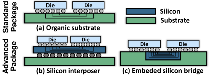
The core of chiplet architecture lies in packaging technologies that facilitate D2D communication, with typical forms shown in Figure 1. Standard packaging connects dies through traces on organic substrates [65, 24], which is cost-effective but results in relatively low bandwidth. By introducing silicon as the fabric for routing, advanced packaging can achieve higher interconnect density and lower power consumption. Two representative approaches are silicon interposers [19] and embedded silicon bridges [32]. The interposer-based packaing introduces a silicon layer with area comparable to the entire chiplet, allowing for flexible routing between dies in different locations. However, when the number of dies becomes very large, its manufacturing cost increases significantly, making it less scalable for larger systems. On the other hand, embedded silicon bridges connect only adjacent dies, resulting in lower costs and better scalability. However, this approach sacrifices interconnect flexibility, as long-distance transfers require multiple hops to be realized. The bandwidth of each D2D link is computed as a multiplication of transfer rate and interface width.
II-B Transformer Workload
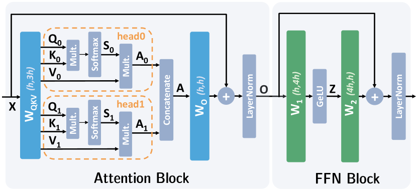
LLMs are composed of several Transformer layers stacked together, each containing an Attention block and a Feed-Forward Network (FFN) block as shown in Figure 2. Most activations are tensors with three dimensions: batch size (), sequence length (), and hidden size (). During training, both and are adjustable configurations, while is determined by the model and reflects the Transformer’s representational capacity.
In Attention blocks, input multiplies with weight matrix to generate three types of activations: query (), key (), and value (). These activations are divided into multiple segments along the hidden size, forming different heads. Each head computes a scaled dot-product attention and , where subscript indicates the head index and is a scaling factor. from all heads are concatenated to form , which then undergoes a linear transformation with weight and adds passed by the residual link. Layer normalization (LayerNorm) is performed to improve training stability. Notably, unlike linear layers with trainable weights, the operands in the attention mechanism are dynamically generated during each forward pass.
FFN blocks consist of an up-scaling and down-scaling linear layer, with a non-linear function like GeLU inserted between them. The intermediate activation ’s hidden size is often scaled four times. Each FFN block also includes a residual connection and a normalization layer.
II-C Parallel LLM Training and Finetuning
Parallelism is essential for LLM training and finetuning to reduce computation time and accommodate massive data, which can be futher categorized into data parallelism (DP), pipeline parallelism (PP), and tensor parallelism (TP).
In DP, each device stores a copy of model parameters and processes part of the batch [27]. The weight gradients computed by each device are aggregated to update weights. It speeds up computation without significantly reducing memory usage. PP [20, 36] distributes LLM layers across different devices, effectively reducing memory usage per GPU. However, pipeline bubbles form at the beginning and end of the computation, which hurts hardware utilization.
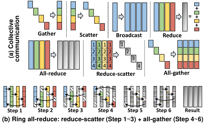
TP divides weight matrices and assigns them to different devices. Collective communications (CC) are necessary to aggregate the results computed by each machine. Typical CCs are demonstrated in Figure 3(a). Depending on the partitioning dimension, TP can be further categorized into 1D-TP such as Megatron [49] and 2D-TP such as Optimus [60]. The CCs they require are listed in Table I.
We display the operations of ring all-reduce algorithm [1] in Figure 3(b). This algorithm splits all-reduce into reduce-scatter and all-gather stages and can achieve full bandwidth utilization. Assume the total data volume is and there are machines, then in each step, each machine transfers a data chunk with the size of to its adjacent in altogether steps. Therefore, transmission time has:
| (1) |
There are other algorithms performing all-reduce. 2D-torus ring executes simultaneous vertical and horizontal ring all-reduce on a 2D-torus topology [33, 63]. Hybrid ring executes grouped and hierarchical transfers, more suitable for layers with less parameters such as CNN [21]. These works are also summarized in Table I.
III System Overview
Section III-A introduces the Hecaton architecture, highlighting its flexibility, scalability, and cost-effectiveness. In order to reduce its corresponding high DRAM access overheads, we optimize its scheduling as demonstrated in Section III-B.
III-A Hecaton Architecture
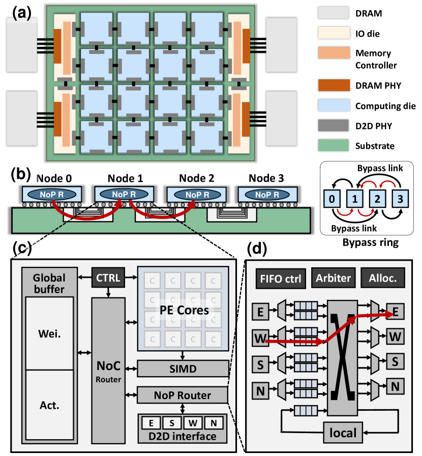
Figure 4 shows a typical system, which comprises the following three main components.
Flexible on-package computation.
Figure 4(c) shows the architecture of the computing die we use in Hecaton. The chiplet design methodology enables a flexible replacement of the computing die with various ASIC accelerators.
Each computing die should consist of the following modules: global weight and activation buffers, a PE array and vector unit for main computation, a NoP router with a corresponding interface, and a controller and network-on-chip (NoC) router for managing intra-die dataflow. The global weight buffers on all dies form a unified on-chip memory pool, together storing parameters of one or more LLM layers. The global buffers in Hecaton are scaled up from those typically used in DNN inference to satisfy the high memory requirements of LLM training, occupying nearly half of the computing die area. This work adopts the classic Simba-like [46] structure, but replacing INT8 multiply-accumulators (MAC) with the FP32 version to support high-precision LLM training. The array can also be replaced with variants supporting sparsity and other dataflows [12, 64, 51, 26], depending on the application. The D2D interface receives or transmits data in different directions and connects to the NoP router, which is introduced later. The NoC router manages communication among PEs and serves as a local interface to the NoP router.
Scalable on-package communication.
D2D connections and NoP routers within computing dies facilitate the on-package communication. For scalability considerations, we use embedded silicon bridges or organic substrates rather than a complete silicon interposer. As model size grows, the chiplet architecture integrates more dies to provide scaled-out computation power, leading to an expanded package area and high manufacture costs for interposer.
We design low-latency bypass links and high-throughput NoP routers that provide setup for scalable communication. Our distributed method (Section IV) requires a ring topology for dies in each column or row. We propose to implement the ring using bypass links as shown in Figure 4(b). Compared to the conventional 2D-torus which directly connects dies at two ends, the bypass ring reduces the longest-link latency from the side length to 2 times the adjacent links.
The router’s architecture is shown in Figure 4(d). It has five ends: local, east (), south (), west (), and north (), managing transmission from various directions. Received packets are buffered in FIFOs and then allocated to a crossbar performing data exchange, overseen by arbitrators and controllers. In the bypass ring, for example, Die 1 not only performs its own data transmission, but also needs to forward data from Die 0 to Die 2. To optimize throughput, we aim to design the router on Die 1 to process these two transactions simultaneously. Observing that the forwarding direction is deterministic—the receive port is always opposite to the transmit port ( to or to )—only wires connecting specific ports and multiplexers for control need to be added, while other modules are reused.
Cost-effective off-package communication.
We employ cost-effective DDR5 DRAMs instead of expensive HBMs as the system’s memory. Under the same budget, DRAMs offer larger storage capacity, which is crucial for LLMs that require extensive memory resources. However, this advantage comes at the expense of reduced bandwidth. To mitigate potential memory access bottlenecks, we employ scheduling techniques which will be demonstrated in Section III-B. The DRAM accesses are managed by IO dies, which contain memory controllers that oversee transactions from different channels. The system’s overall DRAM bandwidth is determined by the product of the number of channels and the bandwidth per channel, with the former being proportional to the package perimeter, and the latter determined by the DRAM type.
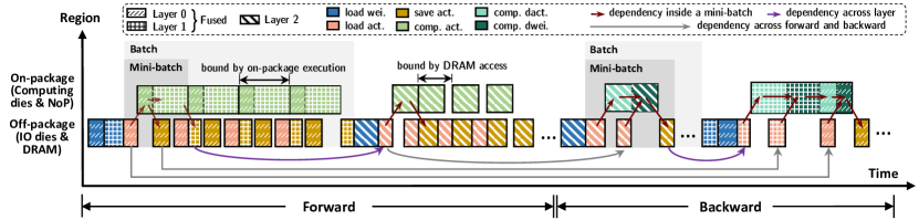
III-B Hecaton Scheduling
We propose the scheduling of Hecaton as shown in Figure 5. Within a training iteration including the forward and backward process of a batch, we divide a batch into multiple mini-batches as minimal execution units. This can help adapt the fixed hardware to arbitrary batch sizes. The larger the activation buffer capacity, the more samples a mini-batch has. The batch size, which infers the number of samples, is specified by the software training strategy; generally, larger batch sizes lead to more stable training.
We allow weights to be reused by multiple mini-batches, so their DRAM access overhead is amortized and accounts for a small portion of the system. However, the DRAM access for activation is still frequent since it is required for each mini-batch. Unlike inference that only needs to save final results, in training the intermediate activations are also saved, as the backward process uses them to compute the gradient of weights. We use the following two techniques to alleviate the impact of DRAM access for activation on system latency.
On-package execution and off-package memory access overlap.
We optimize the throughput by dividing on-package computation / communication and off-package memory access into different pipeline stages, thereby hiding part of the DRAM access latency. The system’s critical path is determined by the longer stage. For example, the fused layer in Figure 5 is bounded by on-packaging execution, while Layer 2 is bounded by off-chip DRAM access. The batch size in training and finetuning is generally kept large to ensure stability, which benefits the pipeline scheduling.
Layer fusion.
With layer fusion [8], outputs of the current layer is directly used as inputs for the next layer, without the process of saving and loading intermediates from DRAM. For example, in Figure 5, Layer 0 and Layer 1 are fused, while Layer 2 is computed separately. A deeper fusion, meaning more layers are executed consecutively, results in a greater reduction in DRAM access. However, the fusion depth is constrained by the capacity of weight buffers. Since the weights of all fused layers need to be stored on-chip, larger weight buffers allow more layers to be fused.
In Transformers, when the weight buffer capacity is tight, all matrix multiplications within the attention blocks are fused, while the two linear layers in the FFN are processed sequentially. This is because the parameter volume of a complete attention block is equivalent to that of a scaling-up or scaling-down FFN layer, both equaling as illustrated in Figure 2. When the weight buffer capacity is sufficient, Attention blocks and FFN blocks can be fused together to further reduce the amount of transferred activation.
IV Distributed Training Method
In this section, we propose a distributed training method to perform computation and NoP communication on Hecaton architecture, i.e., refining the on-package execution part in Figure 5. It can be viewed as a novel tensor parallelism.
IV-A Overview
The distributed training method transforms a single global data communication across all dies into two local communications within dies arranged in the same row or column. These two localized communication phases orchestrate with each other through the 2D mapping of the weight matrix. We carefully design the dataflow to ensure that the localized collective operations only include all-gather and reduce-scatter, which can fully utilize the D2D links on Hecaton. Compared to the tensor parallelism used in Megatron, the volume of activation to be transferred is reduced through the co-design of 2D matrix tiling and communication scheme. Compared to Optimus, our collective operations are more efficient.
We introduce the detailed executions for FFN blocks and Attention blocks in Transformers as follows. It achieves reduced communication complexity, whose formulation will be shown Section V.
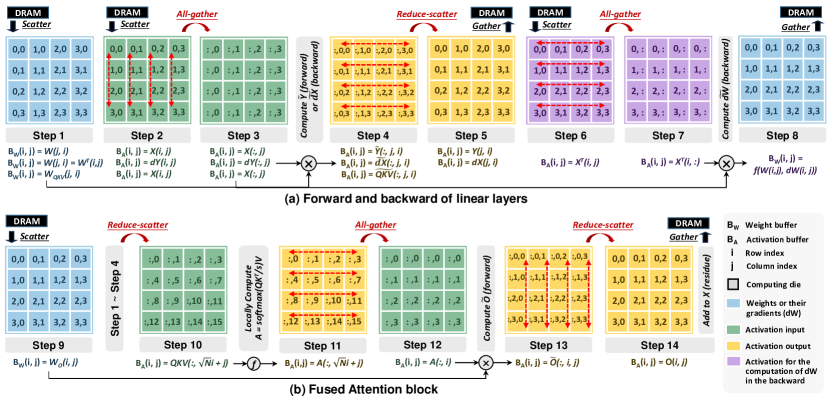
IV-B FFN Blocks
The training process of a single linear layer is outlined in Algorithm 1, with crucial steps illustrated in Figure 6. In each step, communication only happens among dies in the same column or row instead of all dies in the package, thus leading to less communication steps and data to transfer. For software, represents the matrix tiling in the th row and th column, while for hardware, denotes the die’s coordinates. Together, they describe the mapping from tensors to dies. Two details regarding the notation need attention. First, although the activation is three-dimensional (Section II-B), during matrix multiplication, it can be treated as a two-dimensional tensor without affecting the computation results. Second, the notation for partial sums (e.g., and ) is special, involving three elements. The first and last elements still represent the row and column indices, respectively, while the middle element indicates the input channel index of the weight. For example, in , is the partial sum and need to be added together.
One iteration comprises both forward and backward processes, with the latter being more complex due to the computation of . Our dataflow reuses the that has already been all-gathered for the computation of to reduce data transfer, as shown in Figure 6(a). The mapping of tensors is initially designated when tensors are fetched from DRAM, and NoP communication ensures the operands have been prepared in each die’s local buffers before computation.
We make the following optimizations of NoP communication. First, the preparation of input activation () is operated in two steps: scatter from DRAM (Step 2) and all-gather by NoP (Step 3). Compared to fetching X[:,j] from DRAM in a single step, this two-step operation substitutes repetitive expensive DRAM accesses with high-speed and low-energy D2D transfers, thus reducing communication overheads. Furthermore, in our method, NoP only performs two types of collective operations: all-gather and reduce-scatter, both of which can be efficiently executed on the ring topology mentioned in Figure 4(b).
The following paragraph describes the on-package execution when two linear layers are fused. Notably, at the end of the mini-batch’s computation, the tiling of the activation (Step 5) mirrors the transposition of that at the beginning (Step 2). Consequently, the fused layer can be directly computed without additional communication, only requiring to transpose its weight when loading from DRAM (Step 9). An FFN block comprises two linear layers. Therefore, after two rounds of transposition, the input and output mappings are identical, facilitating a direct residual link addition.
IV-C Attention Blocks
Attention Blocks differs from FFN blocks in the multi-head attention, whose executions are explained below. As Figure 6(b) shows, after computing the linear layers that generate (Step 4), the output activation is partitioned along the hidden size dimension instead of the sequence length dimension as in FFN, and then reduce-scattered horizontally (Step 10). This operation ensures that from the same head are processed on the same die, thus utilizing the intrinsic parallelism provided by multiple heads and eliminating inter-die communication. If the number of dies surpasses the number of heads, activation of the same head is saved on different dies, and an all-reduce operation is necessary to compute the complete . Afterwards, an all-gather operation converts the data layout as depicted in Step 12, facilitating the subsequent multiplication with . Step 13 and Step 14 shows operations of the fused layer at the end of the Attention block.
In summary, attention blocks can be viewed as inserting multi-head attention between two fused linear layers with modification of collective operations at the merge points. The backward process of Attention blocks resembles that of FFN, with the key difference being that separate heads are handled by different dies, just like the forward process.
V Theoretical Analysis
This Section provides the formalization of Hecaton’s smaller communication overheads (Section V-A) and proves its weak scaling features (Section V-B). For clarity in subsequent discussions, Table II lists the notations used and their descriptions.
| Notation | Description |
|---|---|
| The number of computing dies on the package. | |
| D2D link latency. | |
| D2D link bandwidth. | |
| The number of DRAM channels. | |
| DRAM bandwidth. |
V-A Formalization
We compare our method with the following three configurations: (1) Flat-ring, which employs 1D-TP and performs ring all-reduce, as used in Megatron [49]; (2) Torus-ring, which also employs 1D-TP but performs 2D-torus all-reduce; and (3) Optimus, which employs 2D-TP and performs broadcast and reduce. 333Given that existing works primarily target GPU systems, we make necessary adjustments to ensure they align with the hardware assumptions discussed in Section III-A.
Communication overheads
| Workload | Link Latency | Transmission Time | ||||||
|---|---|---|---|---|---|---|---|---|
| Flat-ring | Torus-ring | Optimus | Hecaton | Flat-ring | Torus-ring | Optimus | Hecaton | |
| Fwd Atten. | ||||||||
| Fwd FFN | ||||||||
| Bwd Atten. | ||||||||
| Bwd FFN | ||||||||
We decompose the NoP overheads into two parts: link latency and transmission time. The former is a fixed latency for each transmission due to the physical distance, while the latter is the time to transfer data chunks once the connection has been established, calculated as data size divided by D2D bandwidth. For simplicity, we assume that the number of dies is a perfect square.
We first derive the overheads for all-gather (AG) and reduce-scatter (RS) in our method, for link latency and for transmission time. Assuming total data volume is , data with size of are communicated among dies in the same row or column for steps, as illustrated in Figure 3(b). The latency of by-pass links is twice that of adjacent links, as mentioned in Section III-A.
| (2) | ||||
Data volume takes on different values when transferring different activations. Define and , with activations named as in Figure 2, then NoP overheads for the forward pass of Attention blocks and FFN blocks are:
| (3) |
| (4) | ||||
| (5) | ||||
The backward process requires an additional all-gather of the original activations (Step 7), resulting in higher NoP overheads compared to the forward pass. For the Attention block, the extra transfers involve and , while for the FFN block, they involve and . Due to space limitations, we omit the derivation since they are similar to the equation above. The results are summarized in Table III.
The drawbacks of existing methods can be summarized as follows. For 1D-TP, the communication volume is times that of our method. Although 2D-torus provides more links than flat-ring, it can only reduce the constant factor of NoP overheads, not the complexity. For 2D-TP, the execution of broadcast and reduce operations is inefficient because they cannot utilize all available bandwidth. Their derivations can be found in original papers [60, 63, 33].
SRAM Capacity Requirements.
In our method, the maximum SRAM usage occurs when storing the all-gathered activation , whose size is . Therefore, increasing can relieve the memory burden. In contrast, 1D-TP requires storing complete activations such as and with size of on every dies. As the model grows, they can exceed the fixed capacity of SRAM. Optimus needs extra storage for segments broadcast from other dies, further burdening the already capacity-constrained weight buffer.
Layout Constraints.
Our method does not impose specific constraints on the number and layout of dies. Conversely, the flat-ring necessitates an even number of dies to establish the Hamiltonian ring, while Optimus requires a square number of dies. Although the torus-ring method is not constrained by layout as well, it suffers severe performance degradation on rectangular dies due to the imbalanced transmission delay between shorter and longer links.
V-B Weak Scaling Analysis
Our method demonstrates efficient weak scaling, as demonstrated by maintaining nearly constant portions of computation, NoP communication, and DRAM access - the major components of system latency - when scaling both model dimensions and die counts. Specifically, when the model is scaled, the hidden dimension size increases by factor , while the die count increases by .
For computation latency , we can derive Equation (6).
| (6) |
For NoP latency , we have Equation 7. The analysis focuses solely on the transmission time and omitting the link latency, as the latency coefficient is significantly smaller than the bandwidth coefficient , which will be demonstrated in Section VI-E.
| (7) |
For DRAM access , we have Equation 8. We focus on DRAM access for activation and overlook that for weights, because weights are reused across multiple batches, rendering it a minor contributor to system latency, as demonstrated in Section VI-C. The number of DRAM channels grows with the package’s perimeter as explained in Section III-A.
| (8) |
We ensure that the SRAM capacity requirements also remain constant, thus our method will always be valid regardless of the model size. We use and representing the maximal usage of weight buffer and activation buffer.
| (9) | ||||
The enhanced transmission performance of our approach stems from the 2D layout and connection of computing dies. Theoretically, this scheme could extend to GPU-based distributed systems. However, migrating this scheme from Chiplet to GPU clusters would lead to significant performance degradation due to the differences in latency and bandwidth of inter-GPU and inter-server links. Faster links would wait for slower ones, thus harming the utilization of inter connections.
VI Evaluation
VI-A Experiment Setting
Hardware Configurations. Most digital functional modules within the computing die are realized in RTL and synthesized using Synopsys Design Compiler [5], employing 28nm CMOS technology and achieving clock frequencies of up to 800MHz. The non-linear operators are implemented according to previous works [52]. Energy consumption for each module was estimated with PrimeTimePX. The area and read/write energy of SRAM buffers are derived from SRAM Compiler [6]. Attributes for NoP links are sourced from the Universal Chiplet Interconnect Express (UCIe) standards [7] and augmented by prior research [62]. DRAM power and bandwidth are align with the DDR5-6400 [2, 39].
Each computing die incorporates 4096 FP32 MACs arranged in 16 PEs, complemented by a 4MB activation buffer and a 4MB weight buffer. Given the extensive scale of the research problem, we developed a simulator to evaluate our architecture and perform design space exploration based on these source data, adopting a similar methodology of Tangram [17] and Timeloop [41]. Although this paper primarily focuses on the coarse-grained dataflow between dies, the simulator also thoroughly considers the fine-grained mapping and data reuse within each PE to ensure fair energy consumption analysis.
Workloads. We assess the performance of our work across a range of LLMs of varying scales, including Bert-Large [13], BLOOM-1.7B [58], GPT3-6.7B [9], and Llama2-70B [55], with hidden dimensions () equaling 1024, 2048, 4096, and 8192, respectively. We select these models because doubles in them, aligning the weak scaling analysis in Section V-B. Considering that the training and finetuning of larger models are less stable, the batch sizes for these workloads are configured at 16, 32, 64, and 128, respectively. The sequence length is fixed at 512 to accommodate the positional embedding constraints of Bert-Large. As our focus is on the training and finetuning, we are primarily concerned with throughput. Therefore, the latency and energy metrics used in the experiments refer to the latency and energy consumed per iteration of each layer.
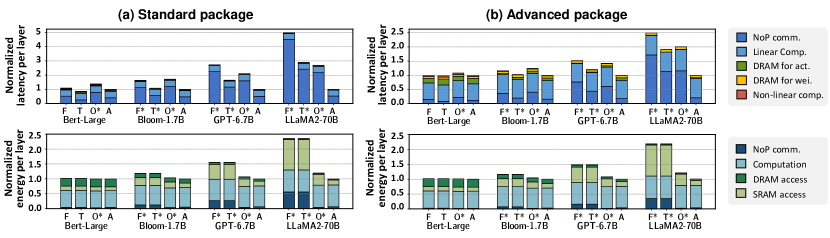
VI-B Overall Comparison
Figure 8 demonstrates that Hecaton has obvious advantages in latency and energy efficiency over other methods across different workloads regardless of the package.
For latency, we achieve at most and speedup when adopting standard package and advanced package, respectively, compared to the tensor parallelism used in Megatron [49]. On larger workloads equipped with more computing dies, Hecaton’s improvement is more obvious, which stems from the reduced NoP overheads. Advanced package offers a higher D2D bandwidth, therefore the NoP communication ratio in the system is also lower than that of standard package. DRAM access for weights only accounts for a small portion as analyzed in Section III-B, supporting its omission in the theoretical analysis in Section V-B. Without scheduling techniques from Section III-B, system latency increases by , with DRAM access for activation comprising over 40
For energy, we achieve at most and improvements correspondingly. Different from latency with NoP communication as the dominates, computation and SRAM access accounts for most of the energy. Both Optimus and Hecaton have an obvious reduction in NoP overheads, since they’re 2D-TP and transfer less data. However, Optimus consumes more energy for SRAM access, which is caused by its fewer data reuse due to operands with smaller size.
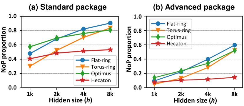
VI-C Weak Scaling
Figure 7 shows the ratio of NoP overheads in the system latency. Bert-Large (), Bloom 1.7B (), GPT3-6.7B (), and LLaMA2-70B () are equipped with 16, 64, 256, and 1024 dies respectively, thus satisfying the weak scaling’s premise. The area of 1024 dies is comparable to that of the WSE-3 by Cerebras [31], justifying the experimental setup is physically feasible.
The results align with the theoretical analysis in Section V-B where the ratio of NoP overheads remains near constant regardless of the model size. In Hecaton, they are mainly affected by the D2D link bandwidth, while those of other methods grow significantly with the model’s scale. The slight growth in Hecaton is caused by link latency , whose impacts will be discussed in Section VI-E.
VI-D Strong Scaling
Our method has better scalability than the tensor parallelism used in Megatron (Flat-ring) when the number of dies increases while the workload is fixed. Other configurations are not compared because their performance degrades significantly when the number of dies is not a perfect square, as analyzed in section V-A. We follow the mapping preferences outlined in experiment VI-F when the layout is not square.
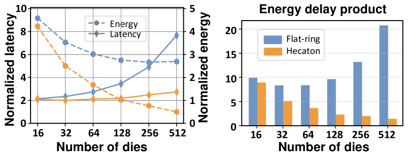
Hecaton’s latency decrease faster and its energy grows slower than Flat-ring, due to its reduced communication overheads. In an ideal strong-scaling scenario, the reciprocal of latency should increase linearly with the number of dies, while energy consumption remains static under a given task. However, in practice, the communication increases when the package integrates more dies, leading to a surge in energy consumption and a diminished latency improvement.
Hecaton’s EDP keeps decreasing, while flat-ring’s EDP follows a first-drop-then-grow trend. Flat-ring achieves the sweet point at approximately 64 dies, implying that attempts to minimize latency come at the cost of increased communication overhead and energy consumption. Conversely, the EDP of our method continues to decline, thus allowing faster training of LLMs by integrating more dies with acceptable energy consumption.
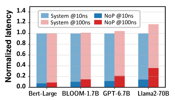
VI-E The Impact of Link Latency
Figure 10 shows the impact of link latency on the whole system is minor. We adopts advanced packaging featuring high bandwidth to minimize the impact of transmission time and highlight the effect of link latency. The impact of ’s increase is most significant when the problem scale is large, because the communication steps grow with the number of computing dies. We observe that even in the most affected case, the NoP overhead of our method only grows by 3, and the overall latency only increases by , far less than the 10 growth in . The growth in NoP overhead is small because the amount of data transferred in each transmission is huge, and the impact of link latency is amortized by the transmission time. The increase in system latency is even smaller than the growth in NoP overheads due to the overlap scheduling, which hides the impact of NoP latency. This analysis supports and justifies the theoretical analysis neglecting link latency in Section V-B.
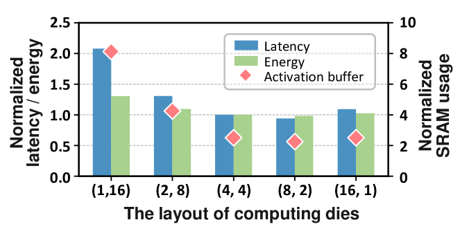
VI-F The Impact of Layout
Hecaton has an obvious preference for layout, as depicted in Figure 11. This arises from the asymmetry in the weight matrix’s dimensions. For example, when performing the scale-up linear layer in FFN blocks, both input and output activation necessitate communication, but the latter is four times the size of the former. Matching the larger activation to a short side leads to transferring large data chunks in fewer communication steps, thus lifting the overall performance. Besides latency and energy, the minimum requirement for activation buffer size also differs. The maximum usage is reached after the all-gather of input activation, whose size is proportional to the side length along which the communication occurs. Therefore, when the larger activation is all-gathered along the longer side, more SRAM capacity is required.
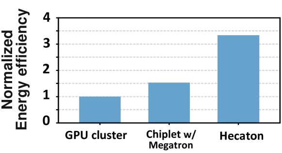
VI-G Comparison with GPUs
We compare Hecaton with GPU clusters under the the Llama2 workload. GPU cluster’s data are derived from paper [55]. Chiplet’s higher energy efficiency stems from the ASIC computing dies designed for specific domains and dense on-package connections. Employing the training method proposed by this paper instead of the tensor parallelism used by Megatron, further improves performance.
VII Related Work
Chiplet-based architecture. Since the release of Simba silicon prototype [65, 66], which aims at scaling DNN inference with Chiplet-based architecture[46], there have been a bunch of works trying to optimize the NoP overheads by designing automatic tools, modeling and working on codesign [53, 53, 18]. There are also works optimizing NoP overheads by designing efficient routing and topologies [61, 62, 15, 16, 25] and deisnging Chiplet scheduling [40, 11, 59]. However, most works are all aimed at traditional DNN or inference, whose computation and memory demand are significantly lower than LLM training and thus cannot be applied to LLM.
LLM training and finetuning. ZeRO [42, 43, 45] designs methods utilizing NVMe for scenarios with limited GPUs. Many works study [20, 29, 36, 37, 30] pipeline parallelism to reduce the overhead of cold-start bubbles Megatron [49] proposed 1D tensor parallelism requiring all-reduce operations. Subsequent works introduce 2D [60] and 2.5D [57] tensor parallelism, which theoretically reduce the complexity of data transfer but impose high requirements on the GPU topology. Current GPU clusters often employ a combination of various parallelisms to accelerate LLM training [44, 50], posing challenges in terms of scheduling strategies [38, 28]. The on-package connections in chiplet have higher density, and our distributed training method has a lower asymptotic communication complexity.
VIII Conclusion
In this paper, we propose Hecaton, a scalable and cost-effective Chiplet architecture for LLM training and finetuning with scheduling minimizing DRAM access impacts. Along with the novel distributed method that co-designs matrix tiling and communication schemes, the system can achieve weak scaling and obtain obvious improvements in both latency and energy compared to previous works.
References
- [1] baidu-allreduce. [online]. Available: https://github.com/baidu-research/baidu-allreduce.
- [2] Ddr5 sdram specification. [Online]. Available: https://www.jedec.org/standards-documents/docs/jesd79-5c.
- [3] The nvidia quantum infiniband platform. [Online]. Available: https://www.nvidia.com/en-us/networking/products/infiniband/.
- [4] Nvlink and nvlink switch. [Online]. Available: https://www.nvidia.com/en-us/data-center/nvlink/.
- [5] Synopsys ip. [Online]. Available: https://www.synopsys.com/designware-ip.html.
- [6] Synopsys memory compilers. [Online]. Available: https://www.synopsys.com/dw/ipdir.php?ds=dwc_sram_memory_compilers.
- [7] Universal Chiplet Interconnect Express (UCIe) Specification, Revision 1.1, Version 1.0, July 2023. [Online]. Available: https://www.uciexpress.org.
- [8] Manoj Alwani, Han Chen, Michael Ferdman, and Peter Milder. Fused-layer cnn accelerators. In 2016 49th Annual IEEE/ACM International Symposium on Microarchitecture (MICRO), pages 1–12. IEEE, 2016.
- [9] Tom Brown, Benjamin Mann, Nick Ryder, Melanie Subbiah, Jared D Kaplan, Prafulla Dhariwal, Arvind Neelakantan, Pranav Shyam, Girish Sastry, Amanda Askell, et al. Language models are few-shot learners. Advances in neural information processing systems, 33:1877–1901, 2020.
- [10] Jingwei Cai, Zuotong Wu, Sen Peng, Yuchen Wei, Zhanhong Tan, Guiming Shi, Mingyu Gao, and Kaisheng Ma. Gemini: Mapping and architecture co-exploration for large-scale dnn chiplet accelerators. In 2024 IEEE International Symposium on High-Performance Computer Architecture (HPCA), pages 156–171. IEEE, 2024.
- [11] Qinyun Cai, Guoqing Xiao, Shengle Lin, Wangdong Yang, Keqin Li, and Kenli Li. Abss: An adaptive batch-stream scheduling module for dynamic task parallelism on chiplet-based multi-chip systems. ACM Transactions on Parallel Computing, 2024.
- [12] Yu-Hsin Chen, Tushar Krishna, Joel S Emer, and Vivienne Sze. Eyeriss: An energy-efficient reconfigurable accelerator for deep convolutional neural networks. IEEE journal of solid-state circuits, 52(1):127–138, 2016.
- [13] Jacob Devlin, Ming-Wei Chang, Kenton Lee, and Kristina Toutanova. Bert: Pre-training of deep bidirectional transformers for language understanding. arXiv preprint arXiv:1810.04805, 2018.
- [14] Alexey Dosovitskiy, Lucas Beyer, Alexander Kolesnikov, Dirk Weissenborn, Xiaohua Zhai, Thomas Unterthiner, Mostafa Dehghani, Matthias Minderer, Georg Heigold, Sylvain Gelly, et al. An image is worth 16x16 words: Transformers for image recognition at scale. arXiv preprint arXiv:2010.11929, 2020.
- [15] Yinxiao Feng, Dong Xiang, and Kaisheng Ma. Heterogeneous die-to-die interfaces: Enabling more flexible chiplet interconnection systems. In Proceedings of the 56th Annual IEEE/ACM International Symposium on Microarchitecture, pages 930–943, 2023.
- [16] Yinxiao Feng, Dong Xiang, and Kaisheng Ma. A scalable methodology for designing efficient interconnection network of chiplets. In 2023 IEEE International Symposium on High-Performance Computer Architecture (HPCA), pages 1059–1071. IEEE, 2023.
- [17] Mingyu Gao, Xuan Yang, Jing Pu, Mark Horowitz, and Christos Kozyrakis. Tangram: Optimized coarse-grained dataflow for scalable nn accelerators. In Proceedings of the Twenty-Fourth International Conference on Architectural Support for Programming Languages and Operating Systems, pages 807–820, 2019.
- [18] Xiaochen Hao, Zijian Ding, Jieming Yin, Yuan Wang, and Yun Liang. Monad: Towards cost-effective specialization for chiplet-based spatial accelerators. In 2023 IEEE/ACM International Conference on Computer Aided Design (ICCAD), pages 1–9. IEEE, 2023.
- [19] PK Huang, CY Lu, WH Wei, Christine Chiu, KC Ting, Clark Hu, CH Tsai, SY Hou, WC Chiou, CT Wang, et al. Wafer level system integration of the fifth generation cowos®-s with high performance si interposer at 2500 mm2. In 2021 IEEE 71st Electronic Components and Technology Conference (ECTC), pages 101–104. IEEE, 2021.
- [20] Yanping Huang, Youlong Cheng, Ankur Bapna, Orhan Firat, Dehao Chen, Mia Chen, HyoukJoong Lee, Jiquan Ngiam, Quoc V Le, Yonghui Wu, et al. Gpipe: Efficient training of giant neural networks using pipeline parallelism. Advances in neural information processing systems, 32, 2019.
- [21] Xianyan Jia, Shutao Song, Wei He, Yangzihao Wang, Haidong Rong, Feihu Zhou, Liqiang Xie, Zhenyu Guo, Yuanzhou Yang, Liwei Yu, et al. Highly scalable deep learning training system with mixed-precision: Training imagenet in four minutes. arXiv preprint arXiv:1807.11205, 2018.
- [22] Jared Kaplan, Sam McCandlish, Tom Henighan, Tom B Brown, Benjamin Chess, Rewon Child, Scott Gray, Alec Radford, Jeffrey Wu, and Dario Amodei. Scaling laws for neural language models. arXiv preprint arXiv:2001.08361, 2020.
- [23] Joonyoung Kim and Younsu Kim. Hbm: Memory solution for bandwidth-hungry processors. In 2014 IEEE Hot Chips 26 Symposium (HCS), pages 1–24. IEEE, 2014.
- [24] Pradeep Lall and Shrikar Bhagath. An overview of multichip modules. Solid state technology, 36(9):65–72, 1993.
- [25] Sabuj Laskar, Pranati Majhi, Sungkeun Kim, Farabi Mahmud, Abdullah Muzahid, and Eun Jung Kim. Enhancing collective communication in mcm accelerators for deep learning training. In 2024 IEEE International Symposium on High-Performance Computer Architecture (HPCA), pages 1–16. IEEE, 2024.
- [26] Jinmook Lee, Changhyeon Kim, Sanghoon Kang, Dongjoo Shin, Sangyeob Kim, and Hoi-Jun Yoo. Unpu: A 50.6 tops/w unified deep neural network accelerator with 1b-to-16b fully-variable weight bit-precision. In 2018 IEEE International Solid-State Circuits Conference-(ISSCC), pages 218–220. IEEE, 2018.
- [27] Mu Li, David G Andersen, Jun Woo Park, Alexander J Smola, Amr Ahmed, Vanja Josifovski, James Long, Eugene J Shekita, and Bor-Yiing Su. Scaling distributed machine learning with the parameter server. In 11th USENIX Symposium on operating systems design and implementation (OSDI 14), pages 583–598, 2014.
- [28] Shenggui Li, Hongxin Liu, Zhengda Bian, Jiarui Fang, Haichen Huang, Yuliang Liu, Boxiang Wang, and Yang You. Colossal-ai: A unified deep learning system for large-scale parallel training. In Proceedings of the 52nd International Conference on Parallel Processing, pages 766–775, 2023.
- [29] Shigang Li and Torsten Hoefler. Chimera: efficiently training large-scale neural networks with bidirectional pipelines. In Proceedings of the International Conference for High Performance Computing, Networking, Storage and Analysis, pages 1–14, 2021.
- [30] Zhuohan Li, Siyuan Zhuang, Shiyuan Guo, Danyang Zhuo, Hao Zhang, Dawn Song, and Ion Stoica. Terapipe: Token-level pipeline parallelism for training large-scale language models. In International Conference on Machine Learning, pages 6543–6552. PMLR, 2021.
- [31] Sean Lie. Cerebras architecture deep dive: First look inside the hw/sw co-design for deep learning: Cerebras systems. In 2022 IEEE Hot Chips 34 Symposium (HCS), pages 1–34. IEEE Computer Society, 2022.
- [32] Ravi Mahajan, Robert Sankman, Neha Patel, Dae-Woo Kim, Kemal Aygun, Zhiguo Qian, Yidnekachew Mekonnen, Islam Salama, Sujit Sharan, Deepti Iyengar, et al. Embedded multi-die interconnect bridge (emib)–a high density, high bandwidth packaging interconnect. In 2016 IEEE 66th Electronic Components and Technology Conference (ECTC), pages 557–565. IEEE, 2016.
- [33] Hiroaki Mikami, Hisahiro Suganuma, Yoshiki Tanaka, Yuichi Kageyama, et al. Imagenet/resnet-50 training in 224 seconds. arXiv preprint arXiv:1811.05233, pages 770–778, 2018.
- [34] Samuel Naffziger, Noah Beck, Thomas Burd, Kevin Lepak, Gabriel H Loh, Mahesh Subramony, and Sean White. Pioneering chiplet technology and design for the amd epyc™ and ryzen™ processor families: Industrial product. In 2021 ACM/IEEE 48th Annual International Symposium on Computer Architecture (ISCA), pages 57–70. IEEE, 2021.
- [35] Samuel Naffziger, Kevin Lepak, Milam Paraschou, and Mahesh Subramony. 2.2 amd chiplet architecture for high-performance server and desktop products. In 2020 IEEE International Solid-State Circuits Conference-(ISSCC), pages 44–45. IEEE, 2020.
- [36] Deepak Narayanan, Aaron Harlap, Amar Phanishayee, Vivek Seshadri, Nikhil R Devanur, Gregory R Ganger, Phillip B Gibbons, and Matei Zaharia. Pipedream: generalized pipeline parallelism for dnn training. In Proceedings of the 27th ACM symposium on operating systems principles, pages 1–15, 2019.
- [37] Deepak Narayanan, Amar Phanishayee, Kaiyu Shi, Xie Chen, and Matei Zaharia. Memory-efficient pipeline-parallel dnn training. In International Conference on Machine Learning, pages 7937–7947. PMLR, 2021.
- [38] Deepak Narayanan, Mohammad Shoeybi, Jared Casper, Patrick LeGresley, Mostofa Patwary, Vijay Korthikanti, Dmitri Vainbrand, Prethvi Kashinkunti, Julie Bernauer, Bryan Catanzaro, et al. Efficient large-scale language model training on gpu clusters using megatron-lm. In Proceedings of the International Conference for High Performance Computing, Networking, Storage and Analysis, pages 1–15, 2021.
- [39] Mike O’Connor, Niladrish Chatterjee, Donghyuk Lee, John Wilson, Aditya Agrawal, Stephen W Keckler, and William J Dally. Fine-grained dram: Energy-efficient dram for extreme bandwidth systems. In Proceedings of the 50th Annual IEEE/ACM International Symposium on Microarchitecture, pages 41–54, 2017.
- [40] Saptadeep Pal, Daniel Petrisko, Rakesh Kumar, and Puneet Gupta. Design space exploration for chiplet-assembly-based processors. IEEE Transactions on Very Large Scale Integration (VLSI) Systems, 28(4):1062–1073, 2020.
- [41] Angshuman Parashar, Priyanka Raina, Yakun Sophia Shao, Yu-Hsin Chen, Victor A Ying, Anurag Mukkara, Rangharajan Venkatesan, Brucek Khailany, Stephen W Keckler, and Joel Emer. Timeloop: A systematic approach to dnn accelerator evaluation. In 2019 IEEE international symposium on performance analysis of systems and software (ISPASS), pages 304–315. IEEE, 2019.
- [42] Samyam Rajbhandari, Jeff Rasley, Olatunji Ruwase, and Yuxiong He. Zero: Memory optimizations toward training trillion parameter models. In SC20: International Conference for High Performance Computing, Networking, Storage and Analysis, pages 1–16. IEEE, 2020.
- [43] Samyam Rajbhandari, Olatunji Ruwase, Jeff Rasley, Shaden Smith, and Yuxiong He. Zero-infinity: Breaking the gpu memory wall for extreme scale deep learning. In Proceedings of the international conference for high performance computing, networking, storage and analysis, pages 1–14, 2021.
- [44] Jeff Rasley, Samyam Rajbhandari, Olatunji Ruwase, and Yuxiong He. Deepspeed: System optimizations enable training deep learning models with over 100 billion parameters. In Proceedings of the 26th ACM SIGKDD International Conference on Knowledge Discovery & Data Mining, pages 3505–3506, 2020.
- [45] Jie Ren, Samyam Rajbhandari, Reza Yazdani Aminabadi, Olatunji Ruwase, Shuangyan Yang, Minjia Zhang, Dong Li, and Yuxiong He. Zero-offload: Democratizing billion-scale model training. In 2021 USENIX Annual Technical Conference (USENIX ATC 21), pages 551–564, 2021.
- [46] Yakun Sophia Shao, Jason Clemons, Rangharajan Venkatesan, Brian Zimmer, Matthew Fojtik, Nan Jiang, Ben Keller, Alicia Klinefelter, Nathaniel Pinckney, Priyanka Raina, et al. Simba: Scaling deep-learning inference with multi-chip-module-based architecture. In Proceedings of the 52nd Annual IEEE/ACM International Symposium on Microarchitecture, pages 14–27, 2019.
- [47] Debendra Das Sharma, Gerald Pasdast, Zhiguo Qian, and Kemal Aygun. Universal chiplet interconnect express (ucie): An open industry standard for innovations with chiplets at package level. IEEE Transactions on Components, Packaging and Manufacturing Technology, 12(9):1423–1431, 2022.
- [48] Taein Shin, Keunwoo Kim, Hyunwook Park, Boogyo Sim, Seongguk Kim, Jihun Kim, Seonguk Choi, Joonsang Park, Jinwook Song, Jaehyup Kim, et al. Signal integrity design and analysis of universal chiplet interconnect express (ucie) channel in silicon interposer for advanced package. In 2023 IEEE Electrical Design of Advanced Packaging and Systems (EDAPS), pages 1–3. IEEE, 2023.
- [49] Mohammad Shoeybi, Mostofa Patwary, Raul Puri, Patrick LeGresley, Jared Casper, and Bryan Catanzaro. Megatron-lm: Training multi-billion parameter language models using model parallelism. arXiv preprint arXiv:1909.08053, 2019.
- [50] Jaeyong Song, Jinkyu Yim, Jaewon Jung, Hongsun Jang, Hyung-Jin Kim, Youngsok Kim, and Jinho Lee. Optimus-cc: Efficient large nlp model training with 3d parallelism aware communication compression. In Proceedings of the 28th ACM International Conference on Architectural Support for Programming Languages and Operating Systems, Volume 2, pages 560–573, 2023.
- [51] Jinook Song, Yunkyo Cho, Jun-Seok Park, Jun-Woo Jang, Sehwan Lee, Joon-Ho Song, Jae-Gon Lee, and Inyup Kang. 7.1 an 11.5 tops/w 1024-mac butterfly structure dual-core sparsity-aware neural processing unit in 8nm flagship mobile soc. In 2019 IEEE international solid-state circuits conference-(ISSCC), pages 130–132. IEEE, 2019.
- [52] Jacob R Stevens, Rangharajan Venkatesan, Steve Dai, Brucek Khailany, and Anand Raghunathan. Softermax: Hardware/software co-design of an efficient softmax for transformers. In 2021 58th ACM/IEEE Design Automation Conference (DAC), pages 469–474. IEEE, 2021.
- [53] Zhanhong Tan, Hongyu Cai, Runpei Dong, and Kaisheng Ma. Nn-baton: Dnn workload orchestration and chiplet granularity exploration for multichip accelerators. In 2021 ACM/IEEE 48th Annual International Symposium on Computer Architecture (ISCA), pages 1013–1026. IEEE, 2021.
- [54] Hugo Touvron, Thibaut Lavril, Gautier Izacard, Xavier Martinet, Marie-Anne Lachaux, Timothée Lacroix, Baptiste Rozière, Naman Goyal, Eric Hambro, Faisal Azhar, et al. Llama: Open and efficient foundation language models. arXiv preprint arXiv:2302.13971, 2023.
- [55] Hugo Touvron, Louis Martin, Kevin Stone, Peter Albert, Amjad Almahairi, Yasmine Babaei, Nikolay Bashlykov, Soumya Batra, Prajjwal Bhargava, Shruti Bhosale, et al. Llama 2: Open foundation and fine-tuned chat models. arXiv preprint arXiv:2307.09288, 2023.
- [56] Ashish Vaswani, Noam Shazeer, Niki Parmar, Jakob Uszkoreit, Llion Jones, Aidan N Gomez, Łukasz Kaiser, and Illia Polosukhin. Attention is all you need. Advances in neural information processing systems, 30, 2017.
- [57] Boxiang Wang, Qifan Xu, Zhengda Bian, and Yang You. Tesseract: Parallelize the tensor parallelism efficiently. In Proceedings of the 51st International Conference on Parallel Processing, pages 1–11, 2022.
- [58] BigScience Workshop, Teven Le Scao, Angela Fan, Christopher Akiki, Ellie Pavlick, Suzana Ilić, Daniel Hesslow, Roman Castagné, Alexandra Sasha Luccioni, François Yvon, et al. Bloom: A 176b-parameter open-access multilingual language model. arXiv preprint arXiv:2211.05100, 2022.
- [59] Xinfeng Xie, Prakash Prabhu, Ulysse Beaugnon, Phitchaya Phothilimthana, Sudip Roy, Azalia Mirhoseini, Eugene Brevdo, James Laudon, and Yanqi Zhou. A transferable approach for partitioning machine learning models on multi-chip-modules. Proceedings of Machine Learning and Systems, 4:370–381, 2022.
- [60] Qifan Xu and Yang You. An efficient 2d method for training super-large deep learning models. In 2023 IEEE International Parallel and Distributed Processing Symposium (IPDPS), pages 222–232. IEEE, 2023.
- [61] Jieming Yin, Zhifeng Lin, Onur Kayiran, Matthew Poremba, Muhammad Shoaib Bin Altaf, Natalie Enright Jerger, and Gabriel H Loh. Modular routing design for chiplet-based systems. In 2018 ACM/IEEE 45th Annual International Symposium on Computer Architecture (ISCA), pages 726–738. IEEE, 2018.
- [62] Lingxiang Yin, Amir Ghazizadeh, Ahmed Louri, and Hao Zheng. Aries: Accelerating distributed training in chiplet-based systems via flexible interconnects. In 2023 IEEE/ACM International Conference on Computer Aided Design (ICCAD), pages 1–9. IEEE, 2023.
- [63] Chris Ying, Sameer Kumar, Dehao Chen, Tao Wang, and Youlong Cheng. Image classification at supercomputer scale. arXiv preprint arXiv:1811.06992, 2018.
- [64] Zhe Yuan, Jinshan Yue, Huanrui Yang, Zhibo Wang, Jinyang Li, Yixiong Yang, Qingwei Guo, Xueqing Li, Meng-Fan Chang, Huazhong Yang, et al. Sticker: A 0.41-62.1 tops/w 8bit neural network processor with multi-sparsity compatible convolution arrays and online tuning acceleration for fully connected layers. In 2018 IEEE symposium on VLSI circuits, pages 33–34. IEEE, 2018.
- [65] Brian Zimmer, Rangharajan Venkatesan, Yakun Sophia Shao, Jason Clemons, Matthew Fojtik, Nan Jiang, Ben Keller, Alicia Klinefelter, Nathaniel Pinckney, Priyanka Raina, et al. A 0.11 pj/op, 0.32-128 tops, scalable multi-chip-module-based deep neural network accelerator with ground-reference signaling in 16nm. In 2019 Symposium on VLSI Circuits, pages C300–C301. IEEE, 2019.
- [66] Brian Zimmer, Rangharajan Venkatesan, Yakun Sophia Shao, Jason Clemons, Matthew Fojtik, Nan Jiang, Ben Keller, Alicia Klinefelter, Nathaniel Pinckney, Priyanka Raina, et al. A 0.32–128 tops, scalable multi-chip-module-based deep neural network inference accelerator with ground-referenced signaling in 16 nm. IEEE Journal of Solid-State Circuits, 55(4):920–932, 2020.