Arbitrary Waveform Generated Metasurface: A New Paradigm for Direct Modulation and Beamforming Decoupling
††thanks: Xuehui Dong, Bokai Lai, Rujing Xiong, Jianan Zhang, Miyu Feng, Tiebin Mi, Robert Caiming Qiu are with School of Electronic Information and Communication, Huazhong University of Science and Technology, Wuhan 430074, China (e-mail: xuehuidong@hust.edu.cn; bokailai@hust.edu.cn; rujing@hust.edu.cn; zhangjn@hust.edu.cn; fengmiyu@hust.edu.cn; mitiebin@hust.edu.cn; caiming@hust.edu.cn)
National Foundation (NSFC), NO.12141107 supports this work.
Abstract
Information Metasurface, also known as reconfigurable intelligent surface (RIS) has gained significant attention owing to its impressive abilities in electromagnetic (EM) wave manipulation with simple structures. Numerous studies focus on achieving efficient and versatile information transmission using RIS across various fields like wireless communication, radar detection, integrated sensing, and communications, among others. Previous studies demonstrate diverse approaches to achieve reflection modulation by utilizing the superposition of the quantified reflection coefficient (RC) of each unit but suffer from the computing complexity of codebook sequence, the safety of communication, and the flexibility of modulation. To address these challenges, we introduce a novel concept of information metasurface, namely AWG-RIS, which is capable of independently producing arbitrary baseband waveforms and beam patterns through a design that decouples magnitude and phase, without changing the beam pattern. The AWG-RIS functions as a reflection mixer, directly embedding the intended signal into the incoming EM waves. Subsequently, we developed an analysis framework and introduced the waveform factor and beamforming factor into the new model, offering theoretical support for the transition from the control signal to the outgoing electromagnetic wave. Additionally, we unveil the world’s first prototype showcasing passive arbitrary waveform generation while maintaining the beam pattern unaltered. Leveraging the decoupling of direct modulation and beamforming, we explore additional applications in several domains relative to traditional RISs. Finally, we present experiments that confirm the generation of arbitrary waveforms and particular spectrograms.
Index Terms:
Reconfigurable Intelligent Surfaces, waveform generation, AWG-RIS, reflection modulation, direct modulation, backscatter communication, radar spoofing.I Introduction
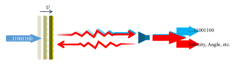
The essence of information is defined as the variations in objects relative to a subject. Electromagnetic (EM) waves serve as the medium that carries these variations in wireless communication systems. Recently, reconfigurable Intelligent Surface (RIS) or information metasurface, comprised of 2D arrays of sub-wavelength reconfigurable units, has attracted great attention due to their remarkable capabilities in manipulating EM wave and their simple structures without radio-frequency (RF) components. RISs can manipulate incident EM waves by altering the distribution of their surface EM characteristics such as reflection coefficients (RC), polarization and spectrum, etc., thereby encoding information in specific parameters of the reflected EM field [1],[2],[3]. The information stems from the controller connected to the RIS, which swiftly modifies the attributes of the reconfigurable units through electrical signals.
I-A Motivation
Considering the baseband electric field (EF) in half-space, it is constituted by the re-radiated EF of each unit of the air-fed RIS. Within one symbol interval,
| (1) |
where the denotes the position vector. In earlier studies, the EF is coupled with both the time domain and the spatial domain, leading to two major issues: first, the variation of the EF differs at various positions ; second, the generation of information depends on the changes in the spatial distribution of the EF [4],[5],[6]. Essentially, this coupling effect arises due to insufficient degrees of freedom (DoF) in controlling the EM characteristic (such as RC) of individual units. To eliminate the coupling effects, we expect that
| (2) |
where the and respectively represent the time-varying and spatially-varying components of the reflected EF of th unit. The former term is responsible for handling information transmission, while the latter term manages the distribution of energy in space. This approach necessitates separating the electromagnetic characteristics with respect to time and space, which aligned with the design principles of the antenna array transmitter [7]. In array transmitter, the capability to radiate electromagnetic waves in specific directions is provided by the phase shifters and power allocators on each antenna in the RF front end [7]. At the same time, the generation of baseband signals involves the baseband signal from the digital-analog convertor (DAC) being combined with the carrier signal produced by the local oscillator through nonlinear components, resulting in the formation of the carrier envelope [8]. This design can make the most of the linear increase in DoF for manipulating electromagnetic waves as the number of antennas rises.
Regrettably, current studies on generating information using RISs have not yet achieved time-space separation manipulation. These studies can be broadly divided into two categories: (1) temporal coding and (2) spatial-temporal coding. The concept of temporal coding has been proposed that manipulates the spectrum of the reflected EM wave while the RC of the metasurface periodically varies [9]. This concept evolves applications such as nonlinear harmonic frequency manipulation [9], independent control of magnitude and phase of the harmonic frequency[10], efficient frequency synthesis[11], multiple polarization transformation [12], non-linear convolution computing [13] and also the wireless communication transmitter [14],[15],[16]. However, the temporal coding does not take into account the energy distribution of the reflected EM wave. To tackle this problem, a metasurface-based spatial-temporal coding theory framework is introduced [17]. This framework concurrently adjusts the spatial energy allocation and the spectral distribution of the reflected electromagnetic wave by jointly encoding discrete RCs in both the time and space domains [4], [5], [6]. This coding approach has been applied in the fields of harmonic beam switching and beamforming [17], multi-bit phase generation [18], Doppler and spectral cloak [19], radio frequency (RF) computing [20], wireless communication [21],[22],[23], cognitive radar [24], generation of orbital angular momentum (OAM)[25],[26], RF imaging [27], etc. However, the coupling of the communication symbols and the radiation patterns hinders its practical use.
These current studies indicate that the baseband signal is typically produced by implementing a specific sequence of beam patterns, resulting in a coupling of information and the beam pattern [9],[4],[5],[6]. Put differently, the data is not modulated into the re-radiated electromagnetic wave but rather encoded in specific positions using particular organized sequences. This introduces three significant and unavoidable challenges:
-
•
The computing complexity of the codebook sequence: Due to the coupling between symbols and beam patterns, the codebook corresponding to each symbol actually depends on the position of the receiving target. In scenarios with multiple targets, non-line-of-sight (NLoS) conditions, and moving targets, it becomes challenging to calculate the required codebook sequences in real time.
-
•
The physical layer security and intercept probability: Because space-time coding entails creating dynamic beam energy distributions, the main lobe of the beam must be in a state of constant change, and the side lobes are also in perennial flux. This variability allows eavesdroppers or non-designated users located in different directions to observe alterations in the beam pattern, thereby elevating the risk of interception and undermining the information’s physical layer security.
-
•
Arbitrary continuous waveform generation: Due to discrete EM characteristics and digital signal control, RISs cannot generate arbitrary continuous baseband signals and spectrogram. This limitation significantly reduces the potential applications of RIS in many fields, such as backscatter devices [28],[29].
To address these challenges, it is crucial to separate the baseband signal generation from the beamforming functions in RIS while concurrently producing the continuous waveform. The core of the first aspect lies in the capability to control the magnitude and phase of the RCs of the RIS elements independently. Changes in the magnitude of the RCs influence the envelope of the emitted EM waves, whereas the phase distribution across the array creates specific beam patterns. The core of the second aspect necessitates the use of DAC, providing continuous control over the bias voltage to achieve direct modulation of the diode. For example, a DC bias is used on an equivalent distributed Schottky diode, which allows for direct modulation of the amplitude of a continuous wave microwave signal [30]. Some reflection amplifiers [31] have also been considered to provide continuous and arbitrary RC values, such as the tunneling diode [32], the varactor diode [33], and the junction-gate field-effect transistor (JFET) [34].
I-B Main contributions
To address the deficiency of existing work, we consider a 1-bit patch antenna RIS with one PIN diode, and propose a new paradigm of RIS, i.e. AWG-RIS, which decoupled the arbitrary baseband waveform generation and beamforming functionality with a low-cost and novel structure. Our main contributions are summarized as follows:
-
•
We propose the AWG-RIS that has a decouple-oriented unit design and a functionality-separated control structure. In particular, the magnitude of the well-designed unit RC can be continuously manipulated by the analogue control signal with a stationary phase while the PIN diode is conducting. Utilizing the analog switches, the analog control of waveform generation and the digital control of beamforming can be separated into individual module that has different performance in accordance with the practical demand. The AWG-RIS can independently generate arbitrary continuous waveforms and beam patterns.
-
•
We propose an analytical framework and introduce two factors into the AWG-RIS model which provide theoretical support for the flow from the control signal to the reflected EM wave. The impulse response of the control circuit and the non-linear characteristic of the diode represent the limitation and distortion of the reflective baseband signal compared to the input signal. New dimension has been developed by the introducing of the independent waveform factor in new model. We also defined the modulation efficiency of AWG-RIS.
-
•
Using the proposed new paradigm and analysis framework, we present the world’s first prototype that implements passive arbitrary waveform generation by RIS. In our prototype, the AWG-RIS has 1-bit quantization of phase and eight inputs of the control signal. The prototype validates the decoupled functions of waveform generation and beamforming. With different numbers of inputs, the prototype can generate arbitrary waveform in diverse way such as single-input direct generation, and multi-input superimposed generation. On this basis, we discuss the future prospects of the AWG-RIS in certain fields and present several primary demonstrations.
I-C Organization
The reminder of this paper is organized as follows. In Section II, we deconstruct and reconstruct the RIS, including the control circuits and the patch antenna, and illustrate the physical principle of the new paradigm RIS. In Section III, we present the structure and model of the AWG-RIS, and look ahead the promising application of it. In Section IV, we demonstrate the approaches of arbitrary waveform generation with single input and waveform synthesis with multiple inputs. The prototype of AWG-RIS and the validation of arbitrary waveform and spectrum generation are presented in Section V. Finally, Section VI concludes the paper.
II Deconstruction and Reconstruction of RIS
In this section, we propose a framework that can continuously control the magnitude of the RC while keeping the phase constant. Initially, we model the RIS unit, including the control circuits, to derive the RC formulation. The decoupled magnitude-phase method is achieved by exploiting the non-linearity of the PIN diode, which exhibits different equivalent resistance values under varying bias voltages. So that the RIS simultaneously manages the reflected baseband signal, maintaining a consistent beam pattern.
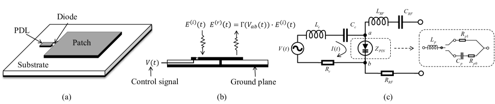
We emphasize the typical configuration of the unit depicted in Fig.1 (a). Earlier studies on metasurfaces primarily address the digital capabilities of PIN diodes, which possess two states: ON and OFF. Depending on various structures, the combinations of PIN diodes in a unit form a set of distinct RC values . The guiding philosophy in designing the RIS’s unit is to maximize the magnitude of these RC values while ensuring an even phase distribution.
When RIS serves as an information metasurface, its capacity to manipulate EM waves should be harnessed to encode data into the incoming EM waves. Maximizing variations in the reflected EM waves is preferred to enhance data transmission. The baseband signal is generated by modifying a meticulously crafted temporal sequence of beam patterns, known as a codebook sequence, a process called temporal-spatial coding. However, for information modulators, this technique presents a trade-off because it cannot independently control the beam and the baseband signal. As a result, the modulation function and the beamforming function are interlinked. To improve modulation flexibility, an advanced RIS design is required that decouples these two functions.
II-A reflection Coefficient of Unit
The integrated equivalent circuits of unit including the controlling part and the RF part is shown in Fig.1 (c). .Earlier studies primarily focus on the RF component, as the control segment is reduced to a simple 0/1 digital signal input. Bit 0/1 corresponds to a fixed input value which makes the voltage across the PIN diode a voltage less or large than the forward conduction voltage . The efficient impedance can be expressed as
| (3) |
where is the equivalent impedance of PIN diode as
| (4) |
Combining with equation (3), we can obtain the expression of RC when the PIN is in forward bias
| (5) | ||||
where is the impedance of free space, and and is respectively the magnitude and phase of RC when the bias voltage of PIN diode is . Similarly, .
II-B Unit as A Reflection Mixer
A PIN diode functions in two distinct modes: forward bias and zero bias. The traditional view has constrained us to employ digital signals for controlling RIS. The inherent nonlinearity of the PIN diode is evident not only in its varying behaviors in forward and zero-bias modes but also in the nonlinear current-voltage relationship during forward bias. In other words, the diode’s equivalent impedance changes with the bias voltage across its terminals, even in forward bias. The relationship between the voltage across the PIN diode and its equivalent impedance can be described by a characteristic function . In conjunction with Eq.(5), it is evident that by applying carefully designed continuous analog signals to control RIS units composed of PIN diodes, the reflection coefficient of the unit can be adjusted continuously.
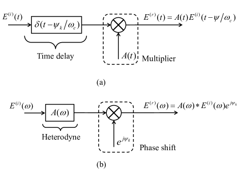
As shown in Fig.1.(b), the unit acts as a passive reflection mixer consisting of one non-linear PIN diode to provide the multiplying terms . The two input signals are respectively the incident EM wave and the time-varying RC . In practice, the voltage across the diode is not exactly equal to the control voltage. As shown in Fig.1.(c), the control circuit can be regarded as an RLC (Resistor Inductor Capacitor) circuit, where and exhibit not only scaling, but also temporal dispersion (frequency selectivity in the spectrum domain). A specific RLC control circuit will cause a certain degree of distortion in the control waveform. We can define a time-invariant impulse response for the control circuit, which accurately represents the relationship between the control signal and the voltage across the diode, i.e.,
| (6) |
The design of is crucial in applications where RIS is used to generate waveforms. We utilize circuit theory to optimize the control circuit, aiming to meet the following two requirements to ensure that the control circuit’s signal is efficiently and undistortedly reflected across the diode’s terminals: (a) The transfer function remains as constant as possible over the baseband signal range; (b) should be as high as possible.
In summary, the accurate reflection of the control signal in the baseband signal requires the combined effect of the control circuit, the characteristic function of the PIN diode, and the design of the unit patch.
II-C Decoupling the Magnitude and Phase of reflection Coefficient
To achieve a higher degree of freedom of modulation (DoF), allowing continuous control of the baseband signal while maintaining the beam pattern, our aim is to decouple the magnitude and phase of RC of the RIS unit. We utilize the fact that the PIN diode’s high-frequency resistance is inversely proportional to the DC bias current through the diode. A suitablely biased PIN diode therefore acts as a variable resistor. The wide intrinsic region also means the diode will have a low capacitance when zero-biased.
This implies that the RC of the unit is a piecewise function w.r.t. . When the diode has zero bias, the reflection coefficient is a stable constant . When the diode is forward conducting, the magnitude of RC becomes , while the phase of RC remains constant and unaffected by the control voltage. It can be expressed as
| (7) |
where the projection is strictly monotone increasing and injective, and are respectively the magnitude and phase of RC at time , is the forward conducting voltage, is the magnitude of RC when the diode is zero bias. Usually, for all .
According to Eq.(3), we learn that the varying resistance values of the PIN diode under different bias voltages affect both the magnitude and phase of the reflection coefficient simultaneously. It is necessary to choose an appropriate structure and a set of parameters for the unit of RIS if we need to keep the phase of RC constant under different bias voltages. As shown in Fig.3, a combination of rectangular patch and PDL was selected, with specific design details referenced from our previous work [35].
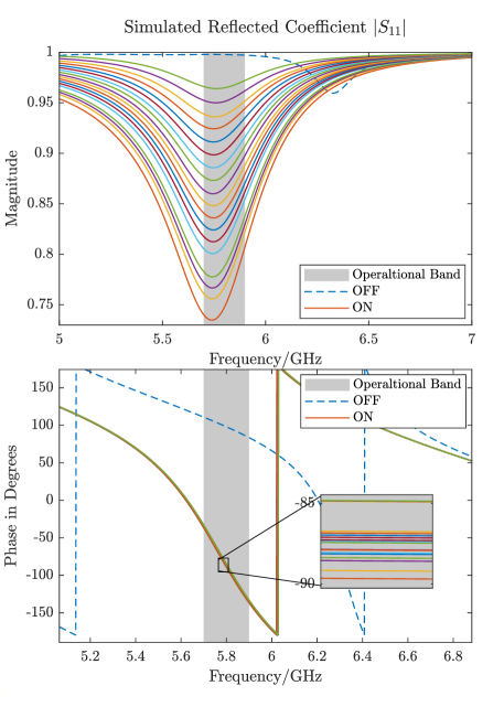
The phase difference is mainly decided by the switching of the PDL. The RC’s magnitude difference depends on the equivalent resistance of the PIN diode. As shown in Fig.4, we set different equivalent resistances for the components that represent the diode in CST studio, resulting in the magnitude and phase of the RC of the RIS unit at different voltages. The 1D result shows that the magnitude of RC continuously decreases as approaches . Equivalently, the larger resistance corresponds to the lower magnitude of RC while PIN diode is conducting. In the mean time, the phase of RC remains almost unchanged.
Remark 1.
Here, an important parameter, the minimum magnitude of the reflection coefficient , largely determines the ability to generate waveforms. is related to the modulation efficiency of amplitude modulation (AM), which reflects the power distribution between the carrier signal and the information signal. When the incident wave power is fixed, a higher enhances the noise immunity of the baseband waveform generated by the RIS. It is shown that the of the unit designed by us is around . Higher modulation efficiency can be achieved by further optimizing the unit structure, circuit design, and the type of diodes used, or even by utilizing transistors. It is found that a high equivalent resistance could reduce the value of due to the approach to the impedance of the free space based on Eq.(5). So, the SMP1345-079LF PIN diode in our unit design could be replaced by another diode with higher resistance.
Assuming we already obtain the mapping operator from the voltage across the diode to the magnitude of the reflection coefficient when the PIN diode is forward biased, the equivalent impulse response of the control circuit and the control signal , then
| (8) |
where and are respectively the magnitude of reflected wave and incident wave, denotes convolution operator.
II-D Decoupling Waveform Generation and Beamforming
Considering a RIS-aided wireless radio channel, the received signal strength is not only depends on the RC of each unit of RIS but also the superposition of all the outgoing wave. In traditional active array antenna transceiver, the beamforming function is achieved through the combined use of phase shifters and power allocators, while the baseband signal is input directly by the feed source. Most reflection modulation works generate the corresponding baseband waveform by utilizing variation of the beam pattern. This is because the magnitude and phase of the reflection coefficient are coupled, significantly reducing the DoF of reflection modulation.
Based on the concept and design of decoupling the magnitude and phase of RC described in the previous section, we could easily decoupling the functions of waveform generation and beamforming on RIS. Given a certain beam pattern and a arbitrary waveform, we generally follow two steps:
-
1.
Determining the discrete phase shift codebook according to the given beam pattern;
-
2.
Calculating the control signal of all the PIN diodes, which are in ON state, according to the given waveform.
Those PIN diodes in OFF state keep a constant magnitude of RC, which do not disturb the generated baseband waveform excerpt for the superposition modulation efficiency.
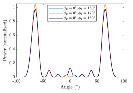
In practical applications and actual design implementations, the phase exhibits minimal jitter, typically within a range of , as illustrated in Fig.4. Due to the quantification of the phase shift, such an error is negligible for a directional beam, as shown in Fig.5. In this result, the directions of the main lobe would not change when the ON-state PIN diodes are biased by different voltages.
III New paradigm of AWG-RIS
In the preceding section, we expounded on the utilization of analog signals to govern specifically designed RIS units comprising 1-bit PIN diodes, facilitating continuous amplitude modulation while preserving the near-constant phase of the RC. This innovation heralds a distinct separation between RIS beamforming and modulation functionalities. Through the introduction of analog signal control, we advocate for a pioneering paradigm shift in RIS technology.
III-A The Structure of AWG-RIS
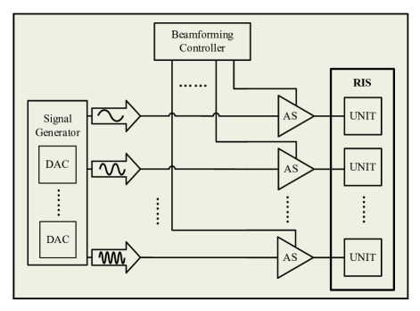
The new paradigm of metasurface decouples the modulation and beamforming functionalities. Each functionality has different performance requirements in different application scenarios. For example, in scenarios aimed at enhancing signals for mobile terminals, beam tracking requires faster beam pattern switching speeds. Conversely, when serving as transmitters (backscatter communication devices), higher sampling rates are demanded from the signal generator’s digital-to-analog converter (DAC). Modulation and beamforming functionalities require control of analog and digital signals, respectively. Therefore, we propose a novel decoupled control approach for RIS, as illustrated in Fig.7.
Within the most general framework, we consider the output of the th analog switch (AS) as the control signal of each unit, with each analog switch’s output determined by a digital enable signal and an analog waveform signal from the th DAC, i.e.,
| (9) |
where , are respectively denoted as the number of units and DACs. . The enable signal actually corresponds to the state of PIN where 0 and 1 are equivalent to OFF and ON. The diagonal matrix is actually the digital codebook of the traditional RIS control framework.
In practice, the number of DACs depends on demand in different scenarios, which is much less than the number of units. Also, DACs could be replaced by certain waveform generated circuits that are cheap and practical. We distinguish between signal generation and beamforming functionalities at the hardware level, enabling more flexible allocation of hardware resources according to specific requirements.
III-B The Model of AWG-RIS
III-B1 unit scattering model
The conventional RIS model is rendered obsolete for systems incorporating the new hardware architecture due to the introduction of the reflection mixer, which is a nonlinear time-variant system as shown in Fig.2. For the convenience of modeling, this paper assumes that units are illuminated by one incident EM wave transmitting from the coordinate . The time-varying waveform denoted by , neglecting the effects of polarization, is considered a narrowband signal. Assuming the origin coordinate is at the geometric center of AWG-RIS, the scattered field of th unit can be evaluated using physical optics techniques by neglecting the edge effects, which can be expressed as
| (10) | ||||
where is the coordinate of th unit, is the central frequency of incident EM wave and denotes the convolution operator. Given a near-field air-fed source position , the coordinate of a far-field receiver can be expressed as where the unit vector of direction . is the delay related to the origin coordinate and is the propagation delay, where
| (11) |
and is the speed of light. and are respectively the magnitude and phase of th unit’s RC . Based on Eq.(9) and Eq.(8), we obtain the definitions of magnitude and phase of RC with respect to beamforming controller module and signal generator module:
| (12a) | ||||
| (12b) | ||||
where and denote the phases at diode state OFF and ON. The Eq.(10) can be written in the Fourier domain as
| (13) | ||||
where is the angular frequency, is the wavenumber vector. The approximation holds under the condition that , i.e., and is a narrow-band signal.
III-B2 planar array scattering model
Considering an AWG-RIS planar array consisting of units, the air-fed is at position . Units are spaced by along the and directions, respectively. We rewrite the EF scattered by unit at th row and th column
| (14) | ||||
where the scattering EF can be separated into two components respectively depending on the wavenumber vector and angular frequency,
| (15a) | |||
| (15b) | |||
Defining
| (16) |
we can write as
| (17) |
The vector incorporates all of the spatial characteristics of the AWG-RIS and is referred to the array manifold vector. The beam pattern is the normalized far-field scattering EF evaluated versus the direction,
| (18) |
where the normalized factor is and the denotes the hermitian operator.
The vector encompasses all the information about the waveform, where the incident EM wave is re-modulated into a waveform resulting from the changes in RC’s magnitude by a mixer-like unit, as shown in Fig.2. We introduce two factor representing the separated functionalities, waveform generation and beamforming:
| (19a) | ||||
| (19b) | ||||
where is the waveform factor and is the beamforming factor, and are defined in Eq.(12). The steering vector of the incident EM wave is
| (20) |
and the the steering vector of the outgoing EM wave is
| (21) |
We rewrite the scattering EF in time-domain by inverse Fourier Transform as
| (22) | ||||
The introduction of separated waveform factor and beamforming factor enhances the flexibility of RIS functionalities.
III-B3 Modulation efficiency
We respectively define two sets with respect to indices of zero-biased and conducting units,
| (23) | ||||
These two sets are complementary to each other, i.e., . According to the workflow described in section.II.D, these two sets and are defined once a specific beam pattern is provided, as well and . [36] gave the conclusions that the beam pattern will not change when the phase shift of each unit gains the same increment. For a 1-bit RIS, given a specific beam pattern, there always exists a codebook such that the set contains more than elements.
To simplify the presentation, we utilize a single subscript for the index. Now we analyze the received baseband signal under the assumption of single-input-single-output. The air-fed source provides a monochromatic EM wave, i.e., carrier, then
| (24) | ||||
where is additional white Gaussian noise (AWGN). We use the beamforming gain to represent the strength gain caused by the antenna phase compensation. The Eq.(24) can be simplified as
| (25) |
The above equation is a reasonable approximation under two condition: (a) the baseband signal bandwidth is much smaller than the center frequency; (b) the aperture size is much smaller than the minimum wavelength of the baseband signal. Based on Eq.(7), the would have modulate the waveform into the EM wave, rather than the that have the constant RC. This implies that the cumulative modulation efficiency will actually fluctuate with changes in the beam pattern,
| (26) |
where is separated as the ac part and the dc part . The affects only the power of the signal carrying the information, not the waveform itself. The dc part of signal is normally filtered by the band-pass filter at receiver. Therefore,
| (27) |
where , and is the length of a symbol. is the modulation attenuation factor.
III-C New Potential of AWG-RIS
Compared to traditional RIS, the AWG-RIS introduces an additional dimension of operation, specifically the waveform of the baseband signal. This additional dimension can be realized by introducing a few economical DACs. The capability of waveform generation extends the potential of RIS, making it more versatile for applications in various fields.
III-C1 Wireless Information Transmission
The number and accuracy of available RCs in an impedance-matching network determine the communication capability of the backscatter tag. Traditional impedance networks can only support a discrete and limited number of RCs. Typically, Backscatter Communication and RIS serve different application purposes: Backscatter Communication is primarily used for data delivery with low energy consumption, while RIS is mainly employed to enhance communication performance in a passive manner[28].
Nevertheless, the AWG-RIS facilitates not just the uninterrupted regulation of RCs but also the separate management of beam patterns. Firstly, unlike conventional backscatter devices, beamforming enhances the signal-to-noise ratio at the receiver. When compared to prior research on RIS modulation, the ability to generate waveforms permits the conveyance of information at the maximum data rate using any modulation method. Additionally, the implementation of a matched filter receiver can help in lowering the symbol error rate.
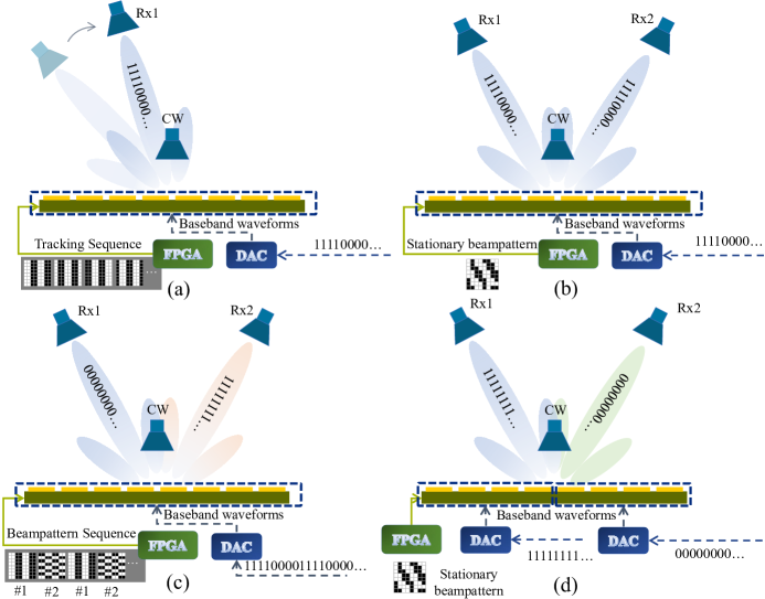
As shown in Fig.8, the beamforming controller is FPGA and signal generator is DAC module. Fig.8.(a) shows that the FPGA only responds for the simultaneous user tracking and the DAC responds for the baseband signal. The computing complexity greatly decreases because the baseband signal is not generated through the variation of beam pattern; Fig.8.(b) shows that the beam pattern with multiple main lobes can serve a multi-user broadcast channel; Fig.8.(c) shows that the beamforming sequence and baseband symbols are jointly designed to achieve time-division multiplexing transmission. Fig.8.(d) shows that the AWG-RIS with two DACs is similar to the MIMO transmitter with two antennas.
III-C2 Radar Spoofing
Arbitrary waveform generation is equivalent to arbitrary time-frequency signature generation, as shown in Fig.16. The AWG-RIS have the ability to imitate objects with any motion pattern that manifests in the micro-Doppler signature. For radars focused on velocity estimation, RIS mounted on object surfaces can deceive the detector by shaping the baseband waveform. Due to its independent control over both the baseband signal and the beamforming pattern, its proficiency in broadband signal modulation significantly surpasses that of conventional RIS.
III-C3 Integrated Sensing and Communication (ISAC)
The AWG-RIS is suitable for the radar-centric communication. The RIS mounted on the object to be detected can embed the communication waveforms into the incident radar waveforms as an envelope. Some of the desired random signals will be remodulated into the deterministic waveform in a form that maintains the necessary sensing performance, as shown in Fig.9. The capability of direct reflection modulation without changing the beam patterns offers an intriguing method to achieve radar-centric communication with greater flexibility.
IV Arbitrary Waveform Generation by AWG-RIS
This section will introduce how to generate an arbitrary waveform with different numbers of DACs in this new paradigm.
IV-A Waveform Generated with Single Input
We hope that the outgoing wave has a baseband signal with the waveform , neglecting the dc part. Assuming there is single input, that is, , each conducting unit’s magnitude of RC can be derived based on Eq.(8). We obtain the output of DAC by
| (28) |
where the denotes the inverse projection of and the . Theoretically, it is enough for RIS to generate arbitrary waveform by only a single input such as DAC. The workflow that how to generate an arbitrary waveform under a specific beam pattern is described in algorithm 1.
Nevertheless, generating a baseband signal with a wide bandwidth using a single input is practically challenging due to the band-pass characteristics of the control circuits’ transfer function . A wideband signal requires a high-bandwidth DAC and a high-performance digital signal processor (DSP), both of which are expensive. This predicament could be tackled by the superposition principle and the reconstruction of waveform.
IV-B Time-frequency Waveform Generation with Multiple Input
The superposition principle derived from Maxwell’s equations forms the foundation of all signal analysis theories. Based on the expression of the baseband signal in Eq.(27), the waveform can be composed by different components with distinct features such as frequency. In order to tackle with the problem mentioned in the previous sections, it is feasible for generating a wide band signal by designing units’ control circuits with distinct pass-bands and integrating them into the RIS.
Time-frequency analysis is the theory that studies the signal whose frequency content changes over time. The short-time Fourier transform (STFT) is a Fourier-related transform that is used to determine the sinusoidal frequency and phase content of local sections of a signal as it changes over time. Conversely, the inverse STFT can also produce a wideband signal composed of multiple frequency components within the corresponding time segment.
Assuming that we have a real wideband baseband signal , due to the symmetry of the spectrum, its frequency range is . This signal is considered to be combined by narrow-band inputs. The symbol length of is ,and the sample rate of signal generator is which is much larger than as the Nyquist’s theorem. So we get a discretized version , where . So the discrete STFT of can be expressed as
| (29) |
where is the frame index, is the frequency bin index, is the hop size, is the point of discrete Fourier transform (DFT) and . is a DFT matrix with a primitive th root of unity . is the window diagonal matrix with the corresponding value of windows in the diagonal line such as Hamming windows. is the generalized Hankel matrix transform which can reshape a vector to a matrix. The DFT matrix is defined by
| (30) |
where the .
The normal hamming windows diagonal matrix ,
| (31) |
where .
The generalized Hankel transform is definde as
| (32) |
where .
The matrix represents the signal spectrogram , where the th column of denotes the spectrum in the th time slot. The th row denotes the th frequency bin of the signal. The bandwidth represented by a frequency bin can be calculated by . Assuming there are nonoverlapping narrow-band inputs, we can express the spectral window diagonal matrix as
| (33) |
where has a 1 at the -th diagonal position, with all other elements being 0. The set has the same frequency bin indices as the corresponding input in terms of rows in . The corresponding frequency bins can be selected by .
The Algorithm 2 demonstrates the process of creating a wide-band waveform by dividing it into multiple narrow-band components using discrete STFT.
V Experimental Validation & Prototype
V-A Prototype
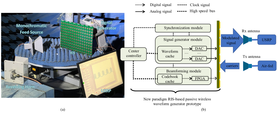
We present the prototype setup of wireless passive arbitrary waveform generation system based on RIS here, which illustrates the hardware design and architecture, including the AWG-RIS prototype and the detailed hardware modules and their roles in the prototype system. The prototype system realizes passive waveform generation with single input, superimposed waveform generation with multiple inputs, and arbitrary spectrogram synthesis over the air. The experimental results demonstrate the feasibility of our proposed paradigm of RIS that decouple the baseband signal and beam pattern.
V-B Prototype Setup
V-B1 AWG-RIS
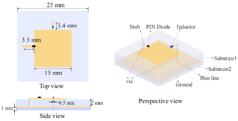
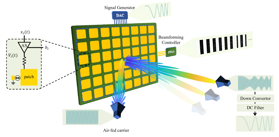
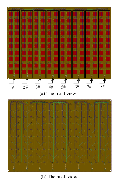
We designed and produced a -unit 1-bit RIS with 8 signal-input SMA-interfaces (i.e., 1#8#) which works at the operating frequency of 5.8GHz, as shown in Fig.11. The upper interfaces is for the digital enable signal from FPGA, which controls the beam pattern of reflected EM wave. The analog switch (MAX4597) is in ON state while the enable voltage is low, the verse is high. The SMA-interfaces on the bottom are the inputs of analog control signal which responds for the manipulation of the RC’s magnitude of each unit so that the baseband signal can be modulated on the reflected EM wave. Each SMA-interface is connected with two nearby columns of units. Within the radiated unit cell, the main metallic patch is connected to the bias line, that is, the output of the AS. To eliminate interference, a choke inductor (LQW15AN19NG00D) is incorporated to isolate the current from the RF signal. The adjacent edge of the patch is connected to the ground through a stub. The stub consists of a specially designed PDL and a PIN diode (SMP1345-079LF), which has a stable equivalent inductance of 0.7 nH and a variant equivalent resistance from tens of ohms to minuteness while the input voltage increases from 700 mV. It is equivalent to a capacitance of 1.8 pF in series with a 0.7nH inductor if the input voltage is less than 700 mV.
V-B2 Signal Generator Module
The signal generator module consists of a waveform cache and multiple DACs. The cache holds the digital data regarding the waveform, provided by the center controller. The center controller ensures that the cache sends the digital data to the appropriate DACs in synchronization with the external clock signal. The DACs then generate the desired waveform into the control circuits as shown in Fig.1.(c). As indicated in Section III.A, the DACs can be substituted with various types of waveform generation circuits.
V-B3 Beamforming Module
The beamforming module consists of a codebook cache and an FPGA. Each FPGA output supplies the enable signal to the AS. High voltage indicates an open state between the output and input of the AS, whereas low voltage indicates a short state. Codebooks for each departure angle could be pre-stored in the cache when the relative position of the air-fed source is fixed. The module takes the current codebook index from the central controller and synchronization signal from an external clock.
V-B4 Center Controller
The center controller is responsible for implementing all algorithms required for waveform calculation and codebook generation across various tasks. Two digital high-speed control signal are output into the signal generator module and the beamforming module according to the results of the algorithm.
V-B5 Synchronization Module
The timing module provides the same reference clock to the center controller module, the signal generator module and the beamforming module.
V-B6 USRP
The USRP platform receive the RF signal from the cable connected with the horn antenna, obtain the baseband signal through the down-converter and send the digital baseband to the host computer. Some necessary signal processes are deployed in host computer of the USRP.
V-B7 Air-fed
The RF air-fed signal is generated by the vector signal source (Keysight N5186A). In our prototype, the air-fed carrier is the 5.8GHz continuous wave. It is worth noting that in practical applications, a low-cost single-tone RF signal source or the EM wave in the environment can provide this carrier signal instead of the expensive RF signal generator instrument.
V-C Experimental Results
As shown in Fig.10 (a), we deployed the prototype in the microwave anechoic chamber that eliminates the interference of environment EM wave. The air-fed horn antenna is approximately 30° to the right of the perpendicular plane of the RIS and at a distance of 50 cm. The receiving antenna is approximately 15° to the left of the perpendicular plane of the RIS and at a distance of 1.5 meters. The purpose of the experiments is to validate the arbitrary waveform generation capability of the AWG-RIS. Therefore, we set up experiments for arbitrary waveform generation and spectrum generation with fixed transmitting and receiving antennas.
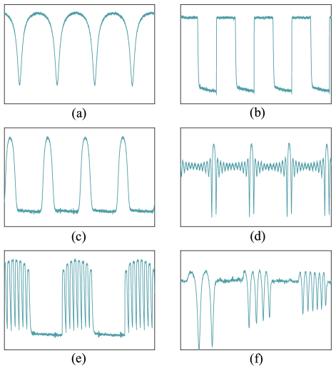
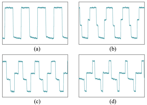
The received baseband waveforms generated by RIS with the aid of single DAC are shown in Fig.12 where the only DAC is parallelly connected with all the inputs (1#8#). We set six common waveforms that are used in communication, radar, and signal processing fields as control signals. These signals underwent responses from the RLC circuit, changes in the voltage-reflection coefficient mapping due to unit nonlinearity, and spatial propagation, and were finally received as baseband signals by the horn antenna. As a clear example, the sinusoid wave signal exhibited nonlinear distortion. This distortion mainly originated from the nonlinear voltage-reflection coefficient mapping of the units since a single-frequency signal is not affected by the RLC circuit. The amplitude range of these control signals is set to a low level of 1V and a high level of 5V, with a frequency of 10 kHz (meaning the same waveform repeats every 100 microseconds). After DC filtering, the amplitude of the received signal is approximately 2 dBm.
As shown in Fig.13, two square waves with the same frequency (i.e. 10kHz) and the same amplitude are combined with four initial phase differences, i.e., 0/45/90/135 degrees. Given that the air-fed source is located in the near-field of the RIS, the incident wave should be regarded as a spherical wave. Consequently, the EM wave energy that arrives at each unit of the RIS varies. The two DACs are alternately connected to the 8 inputs, i.e. the first DAC connected with input 1#, 3#, 5# and 7# (the second one connected with the remainder), which keeps the equality of the energy proportion of two control signals. As shown in Fig.14, we obtain the multiple unusual waveforms stemmed from two elementary waveform and . The findings confirm that implementing analog control endows the RIS with the capability for both direct generation and multi-input superimposed generation of baseband signals.

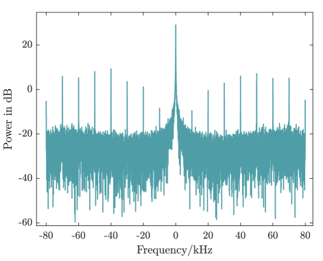
Fig.15 shows the spectrum of the received signal generated by the input of eight different frequency sinusoidal signals. Each sinusoidal input signal has the same amplitude, but the energy at each frequency point in the received signal spectrum is not uniform. This is because the incident wave from the feed source cannot be approximated as a plane wave for the RIS. Therefore, an accurate channel model must be considered when synthesizing baseband signal waveforms. Compared to previous RIS modulation work, where quantized waveforms are generated through phase superposition, resulting in undesirable harmonic components, our proposed framework can produce clean, desired spectrum and waveform.
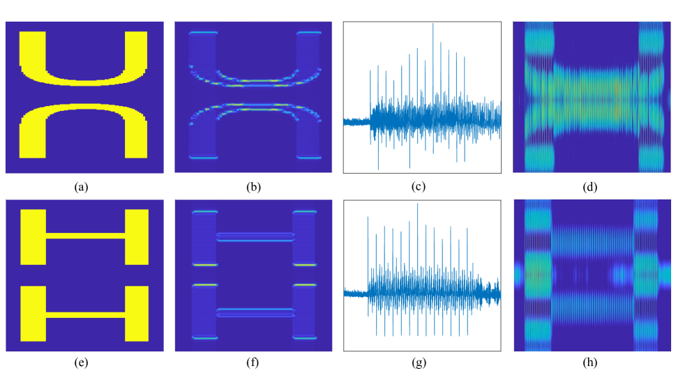
As shown in Fig.16, we utilized a single input to generate a time-frequency spectrum similar to the desired image. First, we generated the desired image, ensuring that it is vertically symmetrical, as we need to produce a real signal whose spectrum is symmetric about the axes. The resolution of the desired image should be matched with the number of samples and points of the discrete Fourier transform. The two-dimension image is equivalent to the spectrogram defined in Eq.(29). The control signal is obtained by inverse STFT and Eq.(28). The air-fed source is a monochromatic continuous wave, and the received baseband signal consists of the dc part, noise, and desired signal. After denoising, DC filtering, and other preprocessing steps, the received time domain signal is transformed using STFT, resulting in the spectrogram shown in the last column of Fig.16.
VI Conclusion
In this paper, we have introduced a novel paradigm for AWG-RIS that features a decoupled unit design and a separated functionality control structure, enabling independent generation of continuous waveforms and beam patterns. We have also presented an analytical framework that includes the impulse response of the control circuits and the nonlinear characteristics of diode-based patches. Additionally, we have proposed a new RIS model incorporating the waveform factor, which adds an extra dimension of operation through the use of a few cost-effective DACs. Furthermore, we have detailed our prototype system, which consists of 1-bit PIN-based units and 8 control signal interfaces. The experimental results demonstrated the capability to arbitrarily create baseband waveforms and spectrograms using a single input and to generate combined outputs from multiple inputs. The positive outcomes highlight the potential of the AWG-RIS in areas such as backscatter communications, radar spoofing, and ISAC. Future research should concentrate on enhancing modulation efficiency and expanding applications.
References
- [1] N. Yu and F. Capasso, “Flat optics with designer metasurfaces,” Nat. Mater., vol. 13, no. 2, pp. 139–150, 2014.
- [2] L. Liu et al., “Broadband metasurfaces with simultaneous control of phase and amplitude,” Adv. Mater., vol. 26, no. 29, pp. 5031–5036, 2014.
- [3] X. Luo, “Subwavelength optical engineering with metasurface waves,” Adv. Opt. Mater., vol. 6, no. 7, p. 1701201, 2018.
- [4] Z. Yu and S. Fan, “Complete optical isolation created by indirect interband photonic transitions,” Nat. Photonics, vol. 3, no. 2, pp. 91–94, 2009.
- [5] A. Shaltout, A. Kildishev, and V. Shalaev, “Time-varying metasurfaces and lorentz non-reciprocity,” Opt. Mater. Express, vol. 5, no. 11, pp. 2459–2467, 2015.
- [6] Y. Hadad, D. L. Sounas, and A. Alu, “Space-time gradient metasurfaces,” Phys. Rev. B, vol. 92, no. 10, p. 100304, 2015.
- [7] E. Biglieri, R. Calderbank, A. Constantinides, A. Goldsmith, A. Paulraj, and H. V. Poor, MIMO wireless communications. Cambridge university press, 2007.
- [8] H. Taub and D. L. Schilling, “Principles of communication systems,” Singapore, 1986.
- [9] J. Zhao et al., “Programmable time-domain digital-coding metasurface for non-linear harmonic manipulation and new wireless communication systems,” Natl. Sci. Rev., vol. 6, no. 2, pp. 231–238, 2019.
- [10] J. Y. Dai, J. Zhao, Q. Cheng, and T. J. Cui, “Independent control of harmonic amplitudes and phases via a time-domain digital coding metasurface,” Light: Sci. Appl., vol. 7, no. 1, p. 90, 2018.
- [11] J. Y. Dai et al., “High-efficiency synthesizer for spatial waves based on space-time-coding digital metasurface,” Laser Photonics Rev., vol. 14, no. 6, p. 1900133, 2020.
- [12] J. C. Ke et al., “Linear and nonlinear polarization syntheses and their programmable controls based on anisotropic time-domain digital coding metasurface,” Small Struct., vol. 2, no. 1, p. 2000060, 2021.
- [13] C. Zhang et al., “Convolution operations on time-domain digital coding metasurface for beam manipulations of harmonics,” Nanophotonics, vol. 9, no. 9, pp. 2771–2781, 2020.
- [14] J. A. Hodge, K. V. Mishra, and A. I. Zaghloul, “Intelligent time-varying metasurface transceiver for index modulation in 6g wireless networks,” IEEE Antennas Wirel. Propag. Lett., vol. 19, no. 11, pp. 1891–1895, 2020.
- [15] W. Tang et al., “Mimo transmission through reconfigurable intelligent surface: System design, analysis, and implementation,” IEEE J. Sel. Areas Commun., vol. 38, no. 11, pp. 2683–2699, 2020.
- [16] J. Y. Dai et al., “Realization of multi-modulation schemes for wireless communication by time-domain digital coding metasurface,” IEEE Trans. Antennas Propag., vol. 68, no. 3, pp. 1618–1627, 2019.
- [17] L. Zhang et al., “Space-time-coding digital metasurfaces,” Nat. Commun., vol. 9, no. 1, p. 4334, 2018.
- [18] ——, “Dynamically realizing arbitrary multi-bit programmable phases using a 2-bit time-domain coding metasurface,” IEEE Trans. Antennas Propag., vol. 68, no. 4, pp. 2984–2992, 2019.
- [19] A. M. Shaltout, V. M. Shalaev, and M. L. Brongersma, “Spatiotemporal light control with active metasurfaces,” Science, vol. 364, no. 6441, p. eaat3100, 2019.
- [20] H. Rajabalipanah, A. Abdolali, S. Iqbal, L. Zhang, and T. J. Cui, “How do space-time digital metasurfaces serve to perform analog signal processing?” arXiv preprint arXiv:2002.06773, 2020.
- [21] Y. Liu et al., “Toward sub-terahertz: Space-time coding metasurface transmitter for wideband wireless communications,” Adv. Sci., vol. 10, no. 29, p. 2304278, 2023.
- [22] J. Yao, J. Xu, W. Xu, C. Yuen, and X. You, “Superimposed ris-phase modulation for mimo communications: A novel paradigm of information transfer,” IEEE Trans. Wireless Commun., 2023.
- [23] G.-B. Wu et al., “A universal metasurface antenna to manipulate all fundamental characteristics of electromagnetic waves,” Nat. Commun., vol. 14, no. 1, p. 5155, 2023.
- [24] Y. He, Y. Cai, H. Mao, and G. Yu, “Ris-assisted communication radar coexistence: Joint beamforming design and analysis,” IEEE J. Sel. Areas Commun., vol. 40, no. 7, pp. 2131–2145, 2022.
- [25] H. Ren et al., “Metasurface orbital angular momentum holography,” Nat. Commun., vol. 10, no. 1, p. 2986, 2019.
- [26] X. Bai et al., “Dynamic millimeter-wave oam beam generation through programmable metasurface,” Nanophotonics, vol. 11, no. 7, pp. 1389–1399, 2022.
- [27] J. Hu et al., “Reconfigurable intelligent surface based rf sensing: Design, optimization, and implementation,” IEEE J. Sel. Areas Commun., vol. 38, no. 11, pp. 2700–2716, 2020.
- [28] T. Jiang et al., “Backscatter communication meets practical battery-free internet of things: A survey and outlook,” IEEE Commun. Surv. Tutorials, 2023.
- [29] J. Kimionis, A. Georgiadis, S. N. Daskalakis, and M. M. Tentzeris, “A printed millimetre-wave modulator and antenna array for backscatter communications at gigabit data rates,” Nat. Electron., vol. 4, no. 6, pp. 439–446, 2021.
- [30] V. F. Fusco and Q. Chen, “Direct-signal modulation using a silicon microstrip patch antenna,” IEEE Trans. Antennas Propag., vol. 47, no. 6, pp. 1025–1028, 1999.
- [31] F. Amato, C. W. Peterson, B. P. Degnan, and G. D. Durgin, “Tunneling rfid tags for long-range and low-power microwave applications,” IEEE J. Radio Freq. Identif., vol. 2, no. 2, pp. 93–103, 2018.
- [32] A. Varshney, A. Soleiman, and T. Voigt, “Tunnelscatter: Low power communication for sensor tags using tunnel diodes,” in The 25th annual international conference on mobile computing and networking, 2019, pp. 1–17.
- [33] R. Reed, F. L. Pour, and D. S. Ha, “An energy efficient rf backscatter modulator for iot applications,” in 2021 IEEE International Symposium on Circuits and Systems (ISCAS). IEEE, 2021, pp. 1–5.
- [34] X. Guo, Y. He, Z. Yu, J. Zhang, Y. Liu, and L. Shangguan, “Rf-transformer: a unified backscatter radio hardware abstraction,” in Proceedings of the 28th annual international conference on mobile computing and networking, 2022, pp. 446–458.
- [35] R. Xiong et al., “Multi-RIS-aided Wireless Communications in Real-world: Prototyping and Field Trials,” arXiv e-prints, p. arXiv:2303.03287, Mar. 2023.
- [36] X. Dong, R. Xiong, T. Mi, Y. Xie, and R. C. Qiu, “Transforming ris-assisted passive beamforming from tedious to simple: A relaxation algorithm for rician channel,” arXiv preprint arXiv:2211.06555, 2022.