pt
jorgestr@ucm.es††thanks: Contributed equally to this paper
jorgestr@ucm.es
Superballistic conduction in hydrodynamic antidot graphene superlattices
Abstract
Viscous electron flow exhibits exotic signatures such as superballistic conduction. Bending the geometry of the device is a must to observe hydrodynamic effects. To this end, we build three antidot graphene superlattices with different hole diameters. We measure their electrical properties at various temperatures and under the effect of a perpendicular magnetic field. We find an enhanced superballistic effect, suggesting the effectiveness of the geometry at bending the electron flow. In addition, superballistic conduction behaves non-monotonically with the magnetic field, which is related with the ballistic-hydrodynamic transition. We also analyze the device resistance as a function of the size of the antidot superlattice to find characteristic scaling laws describing the different transport regimes. We prove that the antidot superlattice is a convenient geometry for realizing hydrodynamic flow, and the experiment provides valuable explanations for the technologically relevant effects of superballistic conduction and scaling laws.
I Introduction
Collisions against impurities and phonons dominate electron-electron collisions in ordinary metals in most cases. In 1963, however, Gurzhi considered the opposite situation and claimed that a decrease in the electrical resistance with increasing temperature might appear in ultra-clean metals at moderate temperatures [1]. This author attributed the phenomenon to the realization of a hydrodynamic regime of charge transport, where highly-correlated electrons behave collectively in a similar way to molecules in conventional viscous fluids [2]. This effect, also known as superballistic conduction, constitutes one of the archetypal hydrodynamic signatures [3, 4, 5, 6, 7, 8, 9, 10]. Moreover, since the collective motion of electrons leads to a resistance below the ballistic limit, superballistic conduction is a convenient property for low-power consumption devices [11]. In this regard, a reduction of the resistance up to has been reported in point contacts [9, 12, 13, 14, 15] and, up to , in crenellated channels [16].
Another well-recognized exotic hydrodynamic signature is the experimental evidence of a Poiseuille flow [8]. In traditional fluids, the Poiseuille law is one of the fundamental principles that affect any fluid network. Its most immediate consequence is a resistance that scales as where is the diameter of a single pipe carrying the fluid [17, 18, 19, 20]. If, instead of a single pipe, the space is filled up with several pipes of diameter the Poiseuille law can be demonstrated to read [18]. Notice that this situation is the equivalent of an antidot superlattice in a two dimensional (2D) system. However, to the best of our knowledge, the equivalent of such scaling law for electrons is not understood in detail.
In the last decade, the development of 2D materials has multiplied the experimental realization of electron hydrodynamics. In this transport regime, electrons travel long distances, larger than the size of typical devices, before scattering against impurities or phonons. This is the case of ultra-pure PdCoO2 [5, 21], Weyl semimetals [22], (Al,Ga)As heterostructures [16] or graphene [8, 9, 6, 7], whose electronic properties dramatically improve when it is encapsulated between two layers of hexagonal boron nitride (hBN) [23]. However, direct visualization of the hydrodynamic flow often requires a complex microscopy setup [8, 10, 24, 22], making it difficult to establish an ubiquitous criterion to establish the occurrence of hydrodynamic transport [8, 7]. Due to the potential applications in electronic design and the need to easily explore new materials [4], it is desirable to look for novel platforms for viscous electron flow.
In this work, we demonstrate that electron trajectories become naturally bent after geometrically engineering the device. This boosts the hydrodynamic signatures, which highly depend on the device size and the non-uniformity of the electron flow. In particular, in this work, we build different antidot graphene superlattices to study superballistic conduction as an indicator of hydrodynamic flow. The experimental setup also allows us to study scaling laws that resemble the traditional fluid Poiseuille law. We also demonstrate a non-monotonic electrical response as a function of the magnetic field, which requires the development of an alternative theoretical understanding. Our experimental evidences are perfectly supported by detailed theoretical simulations that offer a better insight into the fundamentals of superballistic conduction.
II Geometrically-engineered devices for hydrodynamics
Despite the great quality of graphene heterostructures, initial experiments did not find any sign of the expected hydrodynamics regime. Bandurin et al. took an important step forward [6] by noting that the kinematic viscosity enters the Navier-Stokes equation as a coefficient in front of the second spatial derivative of velocity. Therefore, in order to maximize the viscous flow, a current flow as inhomogeneous as possible is needed. Together with the geometry, the edge scattering also needs to be controlled. Recently, the control of the hydrodynamic flow in a 2D electron gas of GaAs quantum wells with smooth boundaries was demonstrated in crenellated channels [16], with reductions of the resistance up to .
In the present work, we design an optimized antidot geometry (see Appendix A) to bend the electron flow and uncover the collective hydrodynamic response of the electrons on a fully encapsulated graphene heterostructure. We perform a cryo-etching process [25] to favor smooth edges that ensure almost specular reflection at the edges and use a graphite bottom gate which enhances the charge mobility. In addition the latter screens undesired spurious effects arising from charged defects present in the underlying doped silicon substrate [26]. This engineered geometry helps us to disentangle viscous and ballistic effects.
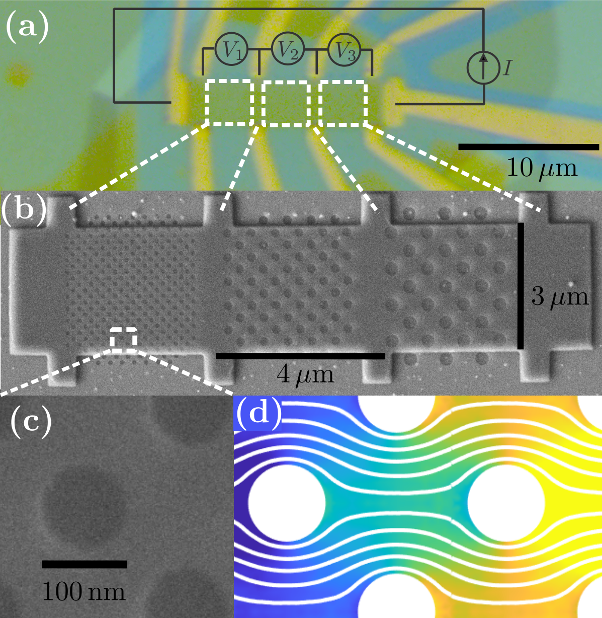
The heterostructure was fabricated by means of the standard mechanical exfoliation on pristine crystals of hBN and graphite, subsequently deposited onto silicon oxide wafer with top p-doped silicon oxide. Then, the stack was finally shaped using e-beam lithography into a typical 10-terminal Hall bar with a longitudinal contact-to-contact distance m, shown in Fig. 1(a). Once the final Hall bar was produced a last step of electron beam lithography + cryo etching [27] process was performed in order to define the antidot patterns as shown in Fig. 1(b) and (c). Three separated regions are shown, consisting of three antidot meshes of different diameters, namely , and . In all three regions, the antidots appear in a square lattice with a center-to-center distance of , defining our final periodic geometry. Fig. 1(d) displays the bent electron trajectories in this geometry. Different dose array tries were performed in order to define pristine structures with an enhanced definition of the antidots (see Appendix B for more details).
III Transport regimes
Viscous electron flow in 2D materials is nothing but a collective motion of conduction electrons that is expected to reduce the device resistance according to Gurzhi’s prediction [1, 2]. In particular, superballistic conduction involves the transition from a ballistic non-collective regime to a collective hydrodynamic one. Consequently, we must use a kinetic model that covers both regimes: the semiclassical Boltzmann transport equation [28, 29] (see Appendix C for a detailed description). Certainly, it is more complex than a hydrodynamic model, but it is the only feasible way to rigorously explore all possible regimes of electronic transport, including the intermediate ones. In our case of interest the Boltzmann equation describing the distribution , which counts the electrons at position moving in the direction of , obeys
| (1) |
where , is the Fermi velocity, and the cyclotron mass, being the Fermi wavenumber in graphene for a density of carriers . The electrons propagate under the effect of a potential and a perpendicular magnetic field with a cyclotron radius . In order to reproduce the experimental scenario Eq. 1 is solved numerically, using a finite element method (Appendix D) to compute the drift velocity as . Finally, the associated current density is integrated to find the current and the longitudinal resistance , which is the electrical property of interest in the experiments.
Equation (1) accounts for different mechanisms of electron collisions that largely affect the electrical response of any material. Collisions with crystal imperfections or lattice vibrations alter the total momentum of the electrons, characterized by the mean free path . We estimate for a gate voltage, referred to the Dirac peak, of , which is a reasonable value after the nanostructuring process of the device [30]. Moreover, we also take into account scattering due to phonons [31, 32] at increasing temperatures (Appendix E). Contrary to impurities and phonons, electron-electron collisions conserve the total momentum, with a mean free path that can be computed for graphene [9, 33]. In this work, we go beyond the conventional Callaway’s ansatz [34] and define two different relaxation rates for the even () and odd-parity () modes in the expansion of . Indeed recent theoretical investigation [35, 36] proves that while , resulting in the so-called tomographic description, which, for the sake of higher accuracy, we follow in this article. Last, there are also collisions against the edges, which are described with the appropriate boundary condition [37]. In our case, the cryo-etching technique produces a smooth boundary, so we assume a perfect slip boundary condition, where electrons have specular reflection at the edges.
The most commonly accepted route towards viscous electron flow is favoring electron-electron collisions to achieve the condition or, more strictly by adding the requirement too, where is the typical size of the device. However, recent works demonstrated these traditional requirements are too restrictive and there exist alternative pathways to achieve the hydrodynamic regime [28].
Although the Boltzmann equation is essential to describe the ballistic-hydrodynamic transition, a hydrodynamic Navier-Stokes equation is the common reference to viscous electron flow [6, 3]. The hydrodynamic equation is expected to provide accurate predictions in the hydrodynamic regime. Conversely, it gives wrong predictions in the ballistic one, so its error can be used to classify the nature of transport [28] and in particular to distinguish between the ballistic and hydrodynamic transport. Regarding the current study, we want to highlight that the superballistic effect will be theoretically and experimentally proven when a ballistic-hydrodynamic transition occurs.
IV Results and discussion
IV.1 Enhanced superballistic effect
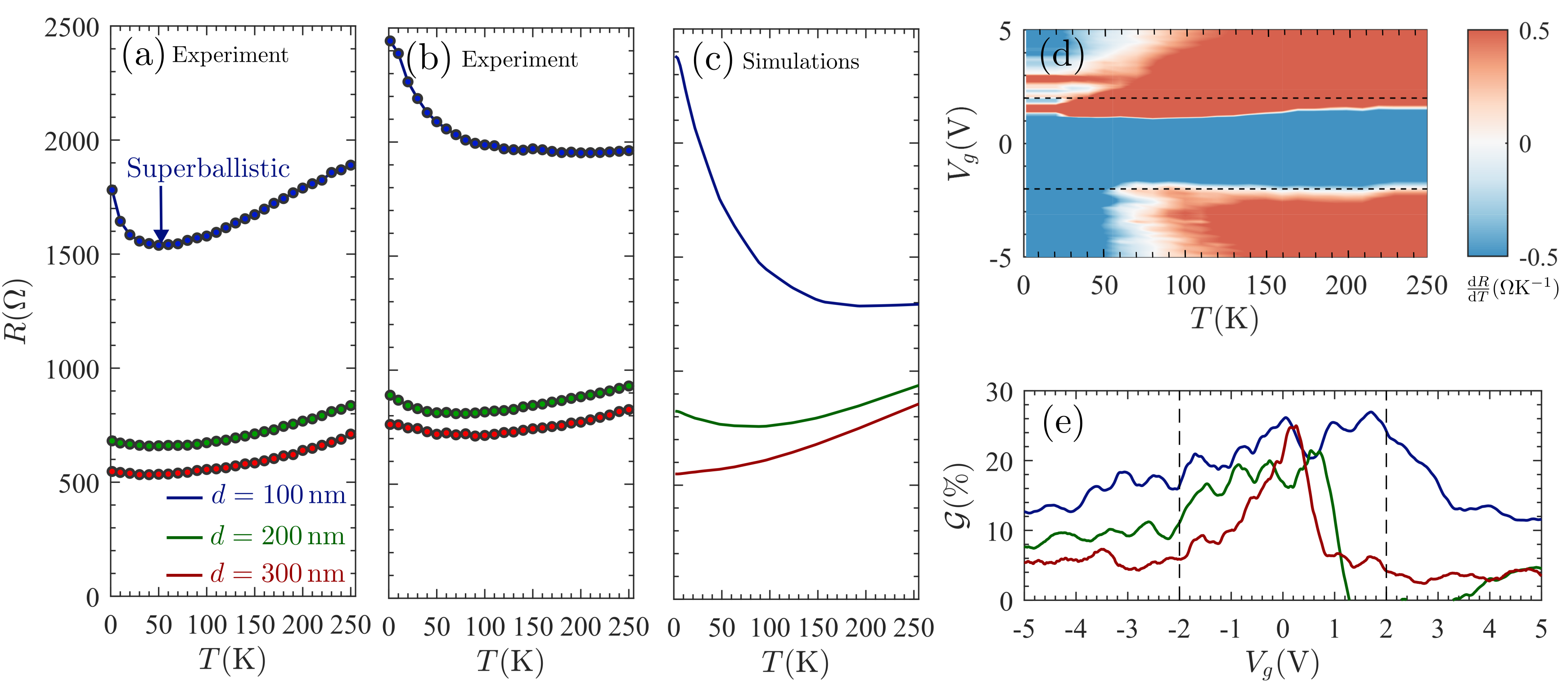
First, we investigate the superballistic effect of the antidot superlattices. Experimental results in Fig. 2(a) and (b) clearly exhibit a decrease in the electrical resistance below its ballistic limit at low temperature in the three antidot regions. Thus, our results demonstrate the existence of the superballistic effect and constitute a signature of hydrodynamic transport. This supports the effectiveness of the antidot superlattice at bending the electron flow. Figure 2(c) shows the predictions of the Boltzmann equation for the same antidot geometries, showing a very good agreement with the experiment. In our simulations, we set the same value nm for the three regions for an easier comparison. Moreover, we have discussed (Appendix F) the influence of possible charge inhomogeneity effects to explain the better agreement with the experiment for hole conduction [see results for in Figs. 2(b) and (c)]. Also, the latter shows an enhanced superballistic conduction in the region of that may survive near room temperature. This result, different from the one observed in the regions of and , had not been reported in point contacts [9]. Nevertheless, it is accurately predicted by the Boltzmann equation. Indeed, both the bending of the electron flow and the smaller restrain the detrimental impact of phonon scattering. Similar to the formation of current whirlpools recently observed in graphene [24], our work is consistent with hydrodynamic effects at room temperature as well. This brings in a paradigm where the technological advantages of reduced electrical resistance can be further exploited. For completeness, Fig. 2(d) monitors the superballistic effect by means of the measured in the region of when the corrected gate voltage and are varied. Notice that hereafter we will refer to as the gate potential defined respect to the Dirac point. Last, Fig. 2(e) shows the magnitude of the superballistic effect estimated as the Gurzhi ratio . This quantity allows us to distinguish the true superballistic effect from other physical scenarios occurring at higher temperatures near the charge neutrality point (within the dashed lines in Fig. 2(d) and (e)), as discussed in Appendix G. Reached ratios of improve those previously reported in point contacts [9]. Once again, this enlarged results as a consequence of the enhanced bending of the electron trajectories by the antidot superlattice. Numerical calculations offer a better insight into the fundamentals of superballistic conduction. Contrary to what was expected, the condition is not essential for the Gurzhi effect to occur [1, 2]. Notice that is indeed very large in the low temperature limit. For example, in our experiment, we demonstrate superballistic conduction even at when while . Furthermore, such a result is supported by our simulations that include the particular geometrical details beyond the approximated anti-Matthiessen rule [9, 15]. The experimental evidence violates the criteria and , so another reasoning must be developed. We conclude that not only the values of and determine the collectivization of the electron flow, but mostly their decrease rate with temperature since . Thus, the existence and the magnitude of the superballistic effect mainly depends of such rates.
In our theoretical study, we also paid attention to the relevance of the boundary conditions to reproduce the experimental results [37] (see Appendix H). Accordingly, we determine that an almost perfect slip condition typical of a specular boundary is compatible with our measurements. This is consistent with the high crystalline quality attained with the cryo-etching technique used in the sample preparation [25] since smooth edges favor the momentum conservation at the boundaries. Similarly to previous works [16], we can conclude that the demonstrated superballistic effect is almost universal since it relies on the geometry of the device and not on the particular considered edge scattering mechanism.
We also check the superballistic conduction in another device where the experimental measurements agree with these results (see Appendix I). More importantly, in the additional device, we demonstrate that there is no decrease in the resistance for a region where no antidots were fabricated. This further confirms that geometrical-engineering is responsible for the observed superballistic conduction.
IV.2 Intermittent superballistic effect
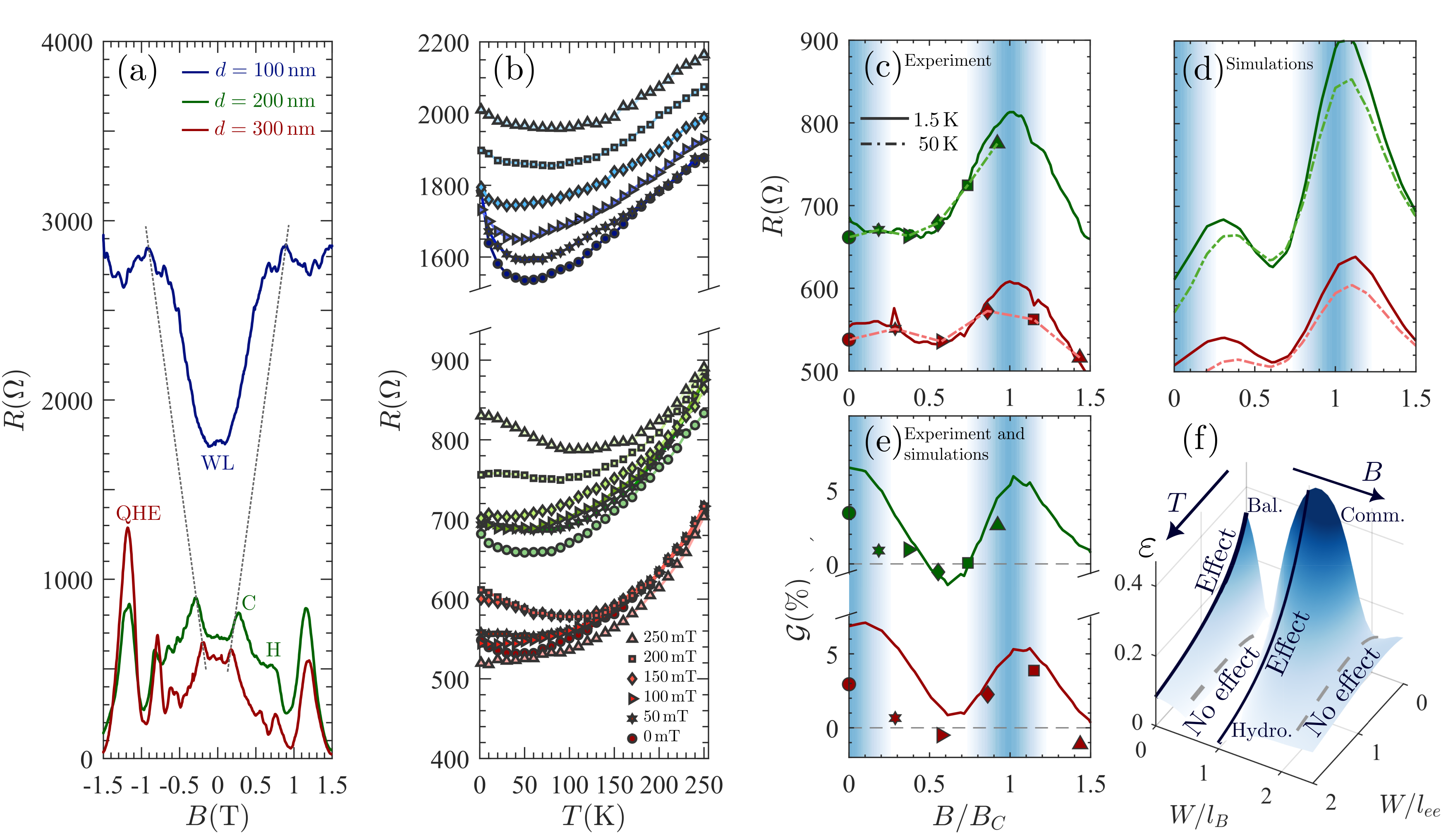
Here we explore the superballistic effect in more detail by considering the electrical response of the antidot lattice in the presence of a magnetic field. First, let us analyze the low-temperature resistance as a function of the applied magnetic field, as shown in Fig. 3(a). Evidence of two quantum effects is shown in our measurements: i) the weak localization peak (WL) at , due to quantum interference [38], and enhanced by intervalley scattering against the superlattice [39] and ii) the quantum Hall effect (QHE), whose peaks flatten for smaller values of , suggesting a prominent role of the antidot geometry. More relevant for the matter of interest are the peaks at the particular field related to the commensurability effect (C), occurring when the cyclotron radius is commensurate to the antidot lattice size [40, 30, 41]. Consequently, these peaks are shifted to higher magnetic fields for increasing as indicated by the dotted line in Fig. 3(a). For and , the hydrodynamic negative magnetoresistance (H) that follows this peak, due to the collectivization of electron flow, is also visible. The region of commensurability is zoomed out in Fig. 3(c) and numerically represented in Fig. 3(d) where the applied magnetic field is expressed in units of .
Regarding the superballistic conduction appearing when the temperature is increased, Fig. 3(b) shows that the effect arises for some magnetic fields and disappears for others, in an intermittent pattern. This is clearly revealed in Fig. 3(e) where the Gurzhi ratio is represented as a function of . Notice the agreement between the experimental measurements and the Boltzmann equation simulations in Figs. 3(c)-(e). Since the considered sizes are much larger than the Fermi wavelength in these devices, the impact of quantum effects is expected to be reduced [40]. Also, the role of the tomographic approach in describing electron transport and its comparison against the hydrodynamic approach is explored in Appendix J, showing that experimental data supports the tomographic approach. The experimental results demonstrate the existence of superballistic transport not only at zero magnetic field as discussed in Sec. IV.1, but also when the magnetic field reaches the commensurability condition. Both cases are consistent with physical scenarios that support a ballistic-hydrodynamic transition as schematically summarized in Fig. 3(f). There we show [28] how the nature of the transport regime is established by way of the deviation of the hydrodynamic model results from the Boltzmann equation. In particular, Fig. 3(f) shows the transition between the ballistic (B) and the hydrodynamic (H) regime when the temperature or the magnitude of a perpendicular field is increased in a uniform graphene channel. Regarding the current study, we want to highlight that the superballistic effect is theoretically and experimentally proven when a ballistic-hydrodynamic transition occurs (notice blue solid lines in Fig. 3(f)). In summary, the superballistic conduction can be used to classify the ballistic and hydrodynamic transport regimes. The conventional formalism based on the Anti-Matthiessen rule [15, 9] does not reproduce the intermittent effect with magnetic field, not even qualitatively, and it had to be replaced by the Boltzmann equation description. Moreover, the classification of the hydrodynamic transition with a magnetic field, which only shows one hydrodynamic region [42], had to be replaced by another one with two hydrodynamic regions, in better agreement with Ref. [28].
IV.3 Quasi-Poiseuille law
The electronic equivalent of the Poiseuille law [20] provides relevant information about the regimes of transport. Let us assume that the resistance of the device scales as such that we could define . For instance, in a purely diffusive regime (), and is the value predicted by the Landauer formula [43, 9]. The physics is more complex when a hydrodynamic description applies in electron systems. Indeed, in Appendix K we find
| (2) |
where is the bending ratio for the antidot geometry and is the viscosity. The expression assumes specular edges, which is a reasonable hypothesis with the cryo-etching technique [25]. Notice that the hydrodynamic description supports all values . This is different from the Poiseuille law in conventional fluids, leading to [18]. Indeed, scattering against impurities and phonons strongly affects the values of , and any finite value of results in . Therefore, it is not , but rather that is assumed as a landmark in electron systems [20]. Nonetheless, the maximum values of occur for shorter , longer , and longer , namely, at low temperatures. Because of the inevitable collisions against impurities and phonons, reducing the viscosity to enter the hydrodynamic regime does not increase , but, on the contrary, diminishes it. Hence, we expect the largest values of near the ballistic regime.
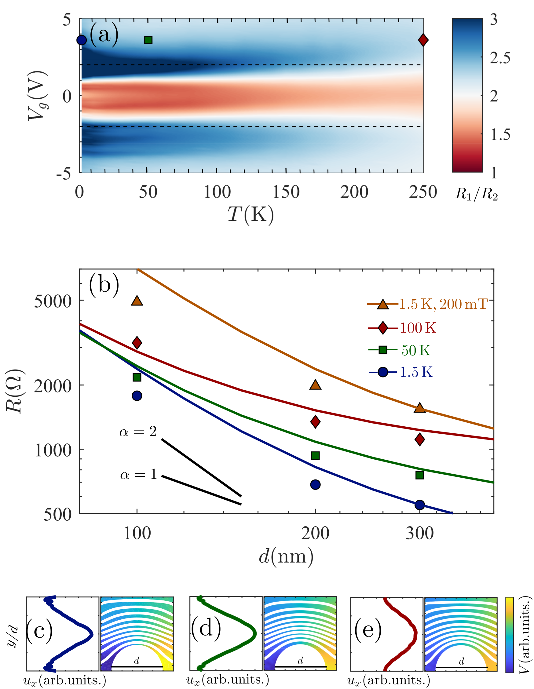
Indeed, this explains the observations in Fig. 4(a), where we plot the ratio between the resistances in the and regions. The maximum occurs at low temperatures and intermediate gate voltages, where the mean free paths of graphene are larger [6].
We study the scaling laws with a Log-Log plot in Fig. 4(b) and compare it with simulations of the Boltzmann equation. Yet simulations improve the accuracy, they show the same qualitative behavior as Eq. (2). Namely, the ballistic regime, whose flow profiles for a paradigmatic set of parameters is shown in Fig. 4(c), gives the largest values of . This regime is approached for low temperatures and shorter . Increasing the temperature favors a transition to a more hydrodynamic regime, for which an archetypal example is shown in Fig. 4(d). Eventually, a diffusive regime, akin to the one in Fig. 4(e), is attained, and . Last, a magnetic field decreases the value of , as it also induces a transition from ballistic to hydrodynamic [28]. In summary, the adapted quasi-Poiseuille law helps us discuss transport regimes. Given the enormous dependence of the electrical properties with , the scaling laws should be taken into account when designing any device.
V Conclusions
We found that the antidot superlattice is a convenient geometry for the realization of electron hydrodynamics. Certainly, the achievement is corroborated by the observation of the superballistic conduction with remarkable Gurzhi ratios (). The antidot geometry bends the electron flow so much that it overshadows the role of edge scattering. So, together with the control of the edge smoothness provided by the cryo-etching technique [25], we obtain an almost universal electron flow [16].
The observed hydrodynamic effects contribute to a better understanding of the hydrodynamic signatures. The simulations of the Boltzmann transport equation account for the ballistic-hydrodynamic transition, and enable us to study the tomographic dynamics of electrons [35]. Thereafter, we improve the conventional hydrodynamic description, and, in particular, the anti-Matthiessen rule that cannot account for our experimental results [15]. Particularly our formalism
based on the Boltzmann equation is crucial to reproduce the intermittent superballistic effect experimentally found as a function of the applied magnetic field.
Our description also sheds light on the classification of the hydrodynamic and ballistic transport regimes, by showing that two collective and hydrodynamic-like regions are achieved in presence of a magnetic field. The existence of collective regions right before and after the commensurability condition is in perfect agreement with the classification of transport regimes in Ref. [28]. Insight into the transport regimes is also attained with the scaling laws.
Both the advantages of the superlattices and the feasibility of their fabrication with lithography open an avenue to further optimize the geometries, look for novel hydrodynamic signatures, and explore materials to reduce the resistance in technological devices.
Acknowledgements.
We wish to acknowledge R. Brito and A. Hamilton for discussions. This work was supported by the “(MAD2D-CM)-UCM” project funded by Comunidad de Madrid, by the Recovery, Transformation and Resilience Plan, and by NextGenerationEU from the European Union, Agencia Estatal de Investigación of Spain (Grants PID2019-106820RB-C21/22 and PID2022-136285NB-C31/C32) and FEDER/Junta de Castilla y León Research Grant number SA106P23. J. E. acknowledges support from the Spanish Ministerio de Ciencia, Innovación y Universidades (Grant FPU22/01039). J. S.-S. acknowledges financial support from the Consejería de Educación, Junta de Castilla y León, and ERDF/FEDER. A. P.-R. acknowledges the financial support received from the Marie Skłodowska Curie-COFUND program under the Horizon 2020 research and innovation initiative of the European Union, within the framework of the USAL4Excellence program (grant agreement 101034371).Appendix A Geometry optimization
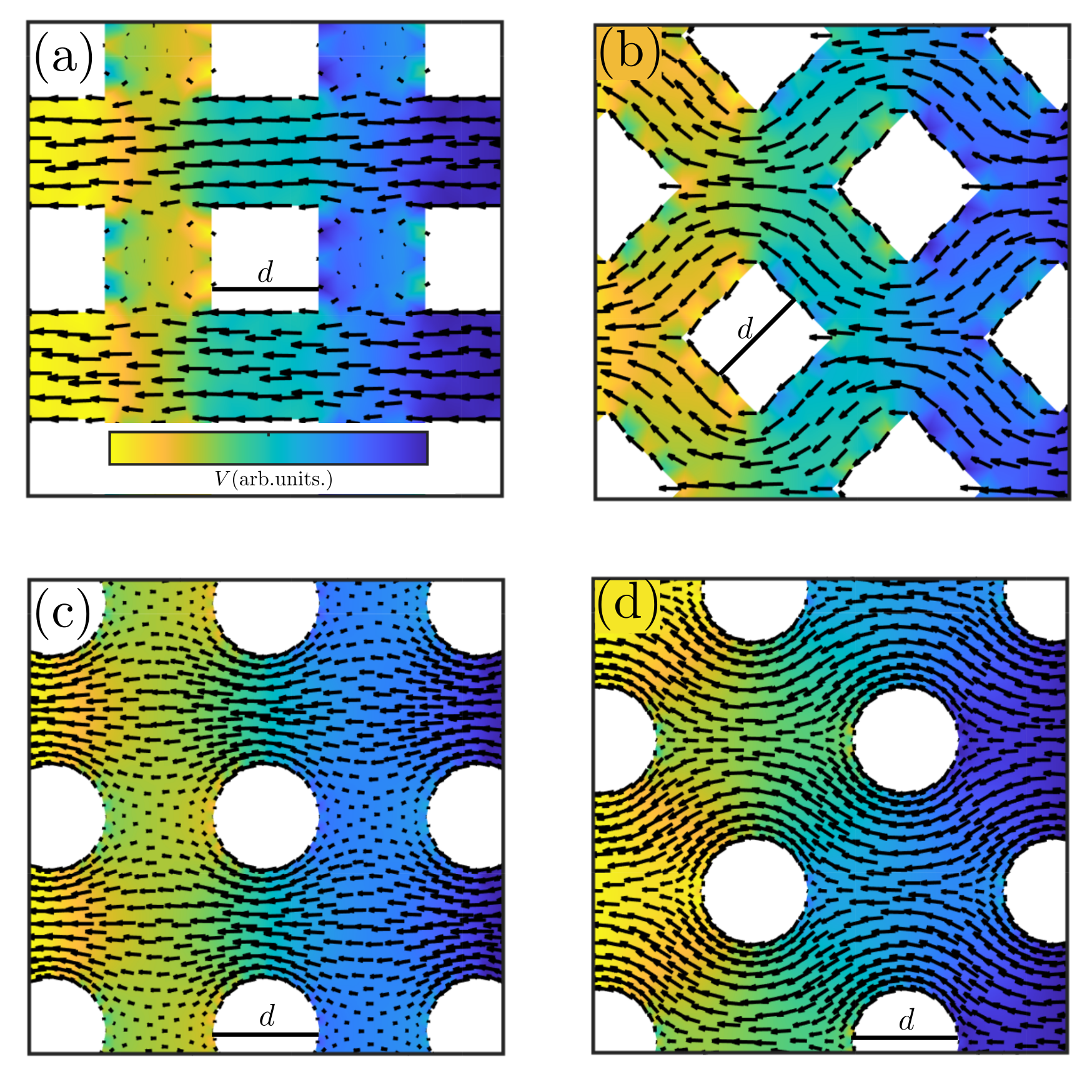
The geometry of a device determines its hydrodynamic properties. Indeed, bending the electron flow enhances the hydrodynamic signatures. Figure S1 shows four antidot superlattices with different configurations and hole shapes, where the device current flows from left to right. These simulations were performed with a hydrodynamic model based on the Navier-Stokes equation for the characteristic lengths and , and perfect slip boundary conditions. In order to quantify the bending of the electron flow in every superlattice, we considered the scaling laws analyzed in Sec. IV, and evaluated the ratio , where is the resistance of a device with antidot size , see Appendix K for a detailed description. Note that is a hydrodynamic signature, so we look for the largest as a quantitative criterion to support a maximized bending of the electron flow. Square antidots have sharp corners, so the electronic fluid follows almost straight trajectories without bending too much, as shown in Fig. S1(a). As a consequence is small. Moreover, given the difficulties in building and simulating samples with sharp corners, we avoid using square lattices. Superlattices with circles as antidots show a higher , especially when they are aligned at respect to the current flow, see Fig. S1(d). In fact, misalignment with the latter avoids straight trajectories, which are less prone to bending around.
Appendix B Sample preparation
The final heterostructure, consisting of a fully encapsulated single layer graphene with a graphite bottom gate was fabricated by means of the standard mechanical exfoliation on pristine crystals of hexagonal boron nitride (hBN) and graphite, subsequently deposited onto a silicon oxide wafer with top p-doped silicon oxide with nominal thickness of 290 nm. Top hBN and bottom hBN flakes had thicknesses of nm and nm respectively and the graphite back gate consisted on a nm-thick layer. The thicknesses of these three layers of the stack were accurately measured with a profilometer model Bruker DekTakXT. For the characterization of the graphene monolayer, micro-Raman spectroscopy for the single-layer material was performed. For the stacking process of the heterostructure, a polycarbonate film was fabricated and deposited on polydimethylsiloxane. Top hBN was picked up at 50-60∘ and deposited on the graphene monolayer at 190∘. Employing the same technique, the hBN bottom flake was deposited onto the graphite back gate. Subsequently, the latter stack was annealed in vacuum at 350∘ to eliminate potential residues. The hBN top and graphene were finally picked up and deposited on the hBN bottom and graphite. A thorough micro-Raman map of the final heterostructure was performed to select the cleanest and defect-free region where the electron-beam lithography was performed.
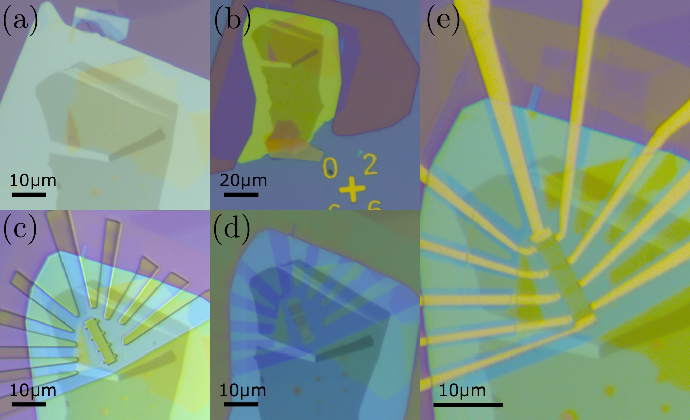
Once the final heterostructure was fabricated (Fig. S2(a)) a premask process was carried out by EBL-SEM to remove excess flakes around it, thus avoiding possible electric shorts between pads and in order to facilitate further processing. A spin coating process was performed using homemade PMMA resist 5 (by weight) in chlorobenzene. The premask was attacked with a cryo-etching system (Fig. S2(b)). Then, the stack was finally shaped by means of e-beam lithography into the final 10-terminal Hall bar (Fig. S2(c)). A subsequent last step of electron beam lithography + cryo etching process was carried out to define the antidot patterns within the Hall bar (Fig. S2(d)). Lastly, 10/55 nm Cr/Au contacts were deposited by e-beam evaporation (Fig. S2(e)) and the device was bonded on a LCC20 chip carrier for electrical characterization, finalizing the sample fabrication.
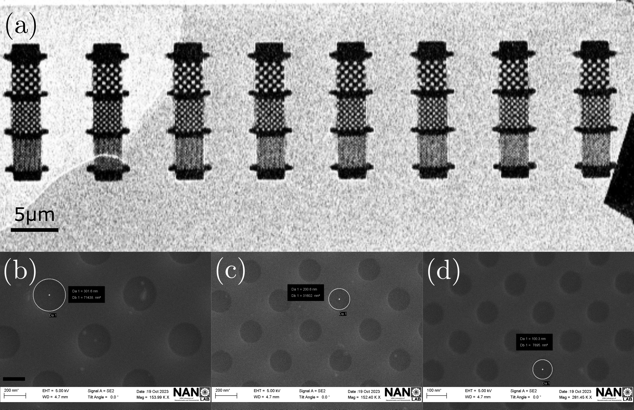
For the crucial lithographic step to define the periodic antidot lattice in the structure, a previous dose array process was carried out into a sacrificial hBN flake replicating the final design as shown in Fig. S3(a). There, doses ranging from 400 to 575 C/cm2 were used showing that 550 C/cm2 generates the optimal resolution for all three different antidot areas as shown in Figs. S3(b)-(d).
Appendix C Theoretical model
Let us describe electrons as semiclassical particles [43, 29, 15], moving in a 2D device with well-defined position and wave vector , where . Let denote the velocity of the electrons. The semiclassical description ignores quantum effects but accounts for the role of the geometry in the hydrodynamic effects. Then the Boltzmann transport equation reads
| (S1) |
where is a perpendicular magnetic field and is a collision operator
| (S2) |
This includes scattering against impurities and phonons, towards the equilibrium distribution with a mean free path and electron-electron scattering towards an equilibrium distribution that moves with the fluids drift velocity. We split this last term with two relaxation times for the even and odd parts of the collision operator [35]. Thus, if is expanded in angular harmonics , is the sum of the terms with even and includes the terms with odd . They have different mean free paths, namely and . Now, let us consider an isotropic conduction band with the Fermi wavenumber, the Fermi velocity and the cyclotron mass. We also assume a constant density of carriers such that , considering valley and spin degeneracy. Importantly, we assume that the relevant phenomena happen near the Fermi surface, so transport can be described just in terms of the direction. Thus, we define
| (S3a) | ||||
| (S3b) | ||||
It is not difficult to show that , where the drift velocity is obtained as . We restrict ourselves to steady-state conditions, such that the non-equilibrium distribution function becomes independent of time. Hence, as described in Ref. [28], the Boltzmann equation for the non-equilibrium distribution function in a potential and a perpendicular magnetic field reduces to Eq.(1).
The geometry and edge scattering plays a crucial role in viscous electron flows, so the Boltzmann equation must be supplemented with the appropriate boundary condition. Two common choices [37, 28] are the diffusive (DF) edge that assumes for all reflected electrons and the partially specular (PS) edge that reads
| (S4) |
where are the reflected electrons and are the incident ones. For the sake of simplicity, we wrote the boundary condition for an edge parallel to . Here, is the dispersion coefficient, with the edge’s bumps mean height and its correlation length. If the edge is almost specular (see Ref. [28] for details of the theoretical model).
Appendix D Numerical methods
We solve the Boltzmann equation numerically with a conformal Galerkin finite element method [44]. We approximate the solution as
| (S5) |
For the spatial part, is the set of tent functions and the products of two tent functions defined on a triangular mesh [45] for the antidot geometry. We impose a maximum triangle size (or under a magnetic field) for which and convergence is ensured. For the angular part, is a set of periodic functions defined on the interval and we use and . We write the weak formulation of (1), add an equation to set a uniform density of carriers and solve the resulting linear system iteratively with a least square approximation in Matlab. At the edges, we impose the boundary condition (S4) for reflected electrons. We solve the system on a rectangular cell of size , and impose periodic boundary conditions. We set the potential difference between two cells across the longitudinal direction, and determine the Hall potential across the transverse direction by adding an additional equation that imposes no net current across the transverse direction. The hydrodynamic model that we used for the geometry optimization was also solved using finite elements [28]. We used a Runge-Kutta 4 method to solve the electronic trajectories in the streamlines, and numerical integration to find the total current. Given the density of carriers which was determined from the quantum Hall effect, the reduced units from the numerical simulation are translated into resistances. The resistances include a geometrical aspect ratio , where is the length of the region containing the antidots and its width, so .
Appendix E Sample characterization
We need to determine the mean free path to characterize the electrical properties of the antidot superlattice. In this section, we show the characterization of the sample and determine the values of .
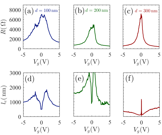
Figure S4(a-c) shows the Dirac peaks for the three regions (, and ) of the device at . Notice the peaks broaden due to the nanostructuring of the device, which can add more impurities and tensions near the edges as well as charge inhomogeneity discussed in Appendix F. Since electron-electron collisions are negligible at this temperature, the device resistance mainly depends on the parameter and the particular lattice geometry. Hence, we can use simulations of the Boltzmann transport equation to estimate the mean free paths that give rise to the experimental resistances. Our results are shown in Fig. S4(d-f), where we find maxima near . Interestingly, this maximum coincides with the maximum of the ratio in the quasi-Poiseuille law, see Fig. 4(a).
We notice that the resistance is mainly determined by the antidot geometry and not by scattering against impurities. On the one hand, this causes the estimated value of to be enormously sensitive to and to the experimental inaccuracies on its measurement, with estimations that may differ for each region. On the other hand, it is an advantage for this experiment, since the exact electrical properties are quite robust, not being very sensitive to .
In the low-temperature limit, we assume at , similar to the one achieved in other graphene nanostructures [30], which also accounts for the additional damage to the structure due to the structuring process. Last, we include phonon scattering, with a Bloch-Grüneisen temperature of to account for the low-temperature non-linear dependence [32]. This assumes that phonons do not affect the electrical properties below and a high-temperature linear dependence [31] of .
Appendix F Charge inhomogeneity
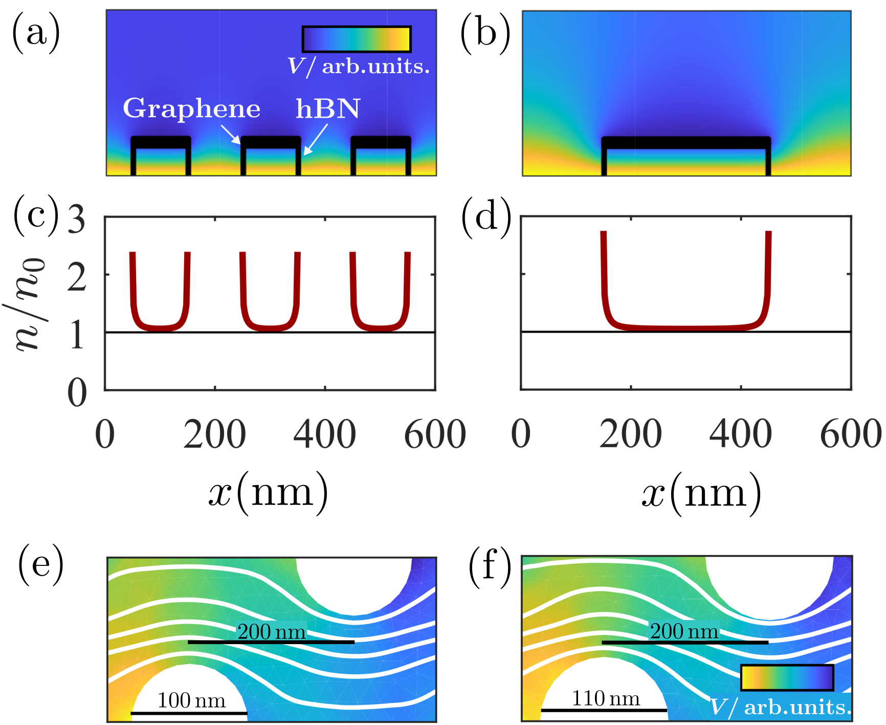
In this experiment, we engineer the geometry of the device in order to bend the electron flow. As a side effect, the back gate induces an inhomogeneous density of carriers . Let us quantify the underlying electrostatic effect for a graphene flake encapsulated between two layers of hBN, a dielectric medium with , with the top and bottom thicknesses of and respectively. For this purpose, we consider a simplified two dimensional problem by assuming that the holes extend across the direction perpendicular to the figure, where we can solve the Poisson equation with a finite differences numerical method. Figure S5 shows the solution: panels (a) and (b) show the electrostatic potential and (c) and (d) account for the induced density of carriers. Indeed, the density of carriers is inhomogeneous, and the accumulation next to the edges would be more relevant for superlattices of shorter .
Charge inhomogeneity flattens the Dirac peak of geometrically engineered samples, shortens the effective mean free paths , and leads to small discrepancies when the same path is used for all the antidot regions. We quantify the effect of charge inhomogeneity by studying the most dramatic scenario where the region adjacent to the holes does not contribute to electrical conduction, for example, when it is depleted of electrons. Therefore, we can simply simulate a system with the same center-to-center distance, but with bigger antidots. The results for archetypal experimental parameters at low temperature and are shown in panels (e) and (f). We find that even a major change of in the antidot diameter only results in a change of in the resistance. Although it is quite remarkable, it is not enough to explain the most relevant results of our work Last, we notice that, due to the doping of the graphene flake with holes, the applied voltage that we need to achieve a density of holes is smaller, in modulus, than to achieve the same density of electrons. Thus, the inhomogeneity is less noticeable when working with holes. This may explain the better agreement with the simulations when working for holes, see Fig. 2(b) and (c). Last, if the scaling laws were caused by the inhomogeneity, they should be dramatically different for electrons and holes. Consequently, the fact that the scaling prevails both for types of carriers (see Fig. 4(a)) indicates that it is not due to charge inhomogeneity.
Appendix G Charge neutrality
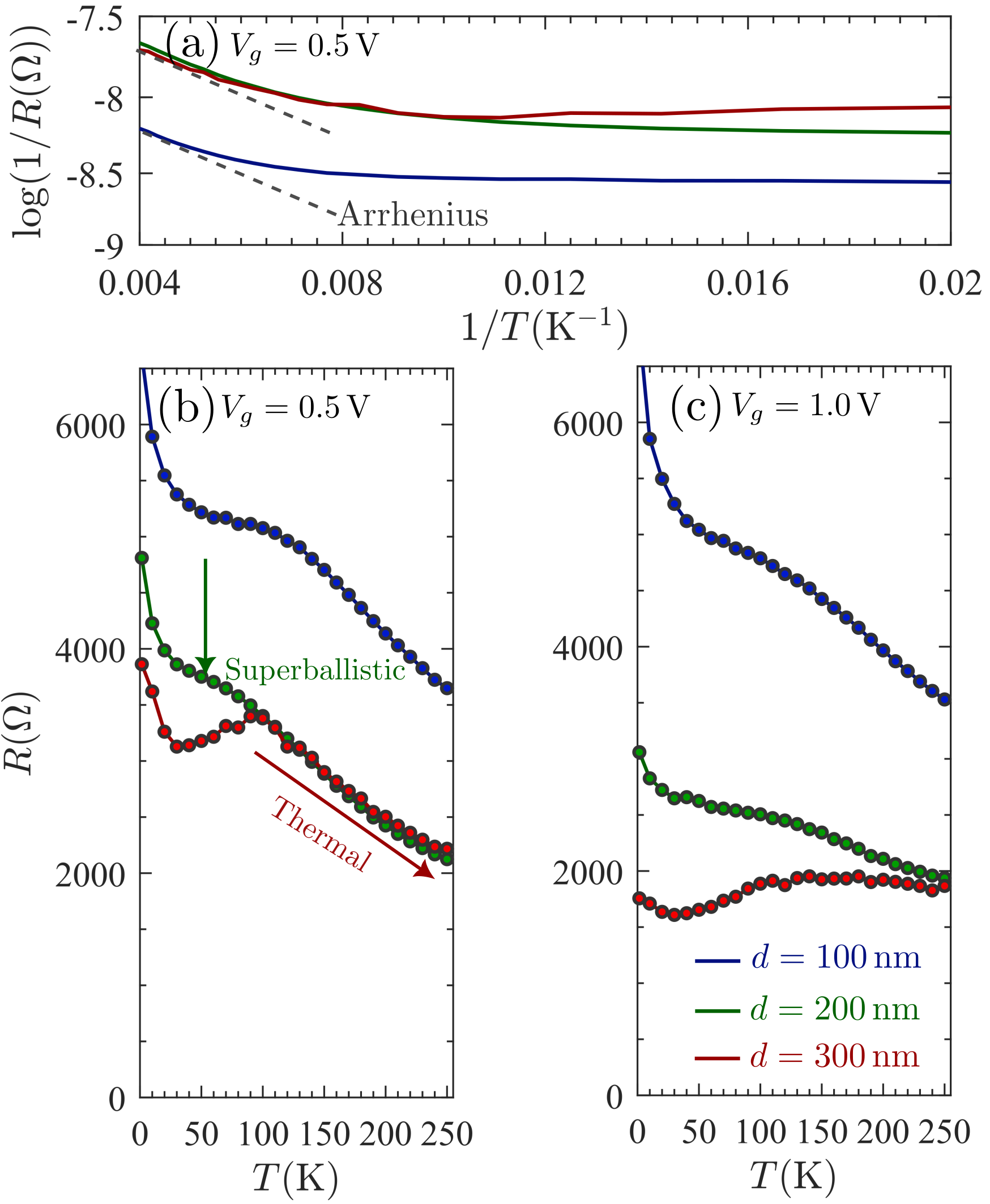
Superballistic conduction is often studied far away from the charge neutrality point [9, 16, 46]. Conversely, in this section, we will focus on superballistic conduction near the charge neutrality point. Figure S6(a) shows an Arrhenius plot near the charge neutrality point. On the one hand, the high-temperature region is dominated by the thermal activation of carriers, as it is characteristic of an intrinsic semiconductor or an insulator. On the other hand, the experimental data does not fit to the Arrhenius law for low temperatures [31], meaning that the low-temperature resistance is not dominated by thermal activation. Indeed, Fig. S6(b) shows two distinguishable steps in the resistance: superballistic conduction occurs at and thermal activation for . Fig. S6(c) accounts for another density of carriers, and it also shows distinguishable superballistic conduction at . Therefore, we conclude that the Gurzhi ratio effectively decouples superballistic conduction from thermal activation.
Appendix H Boundary scattering and universality
One of the main questions regarding electron hydrodynamics is that of the edge scattering, which determines some electrical properties [37]. The cryo-etching technique gives control of the graphene edge, with bumps of mean height and correlation lengths in the order of the nm [25]. Since unless we are next to the Dirac peak, we assume for the dispersion coefficient in the simulations. Indeed, we compute all the results in the article with , which is a practically perfect slip. In this sense, this is the same as the boundary condition for electrostatically defined edges in GaAs heterostructures [16], providing a mechanism for the control of edge scattering in graphene, whose gaplessness does not allow electrostatically defined edges. This provides results in agreement with the experiment.
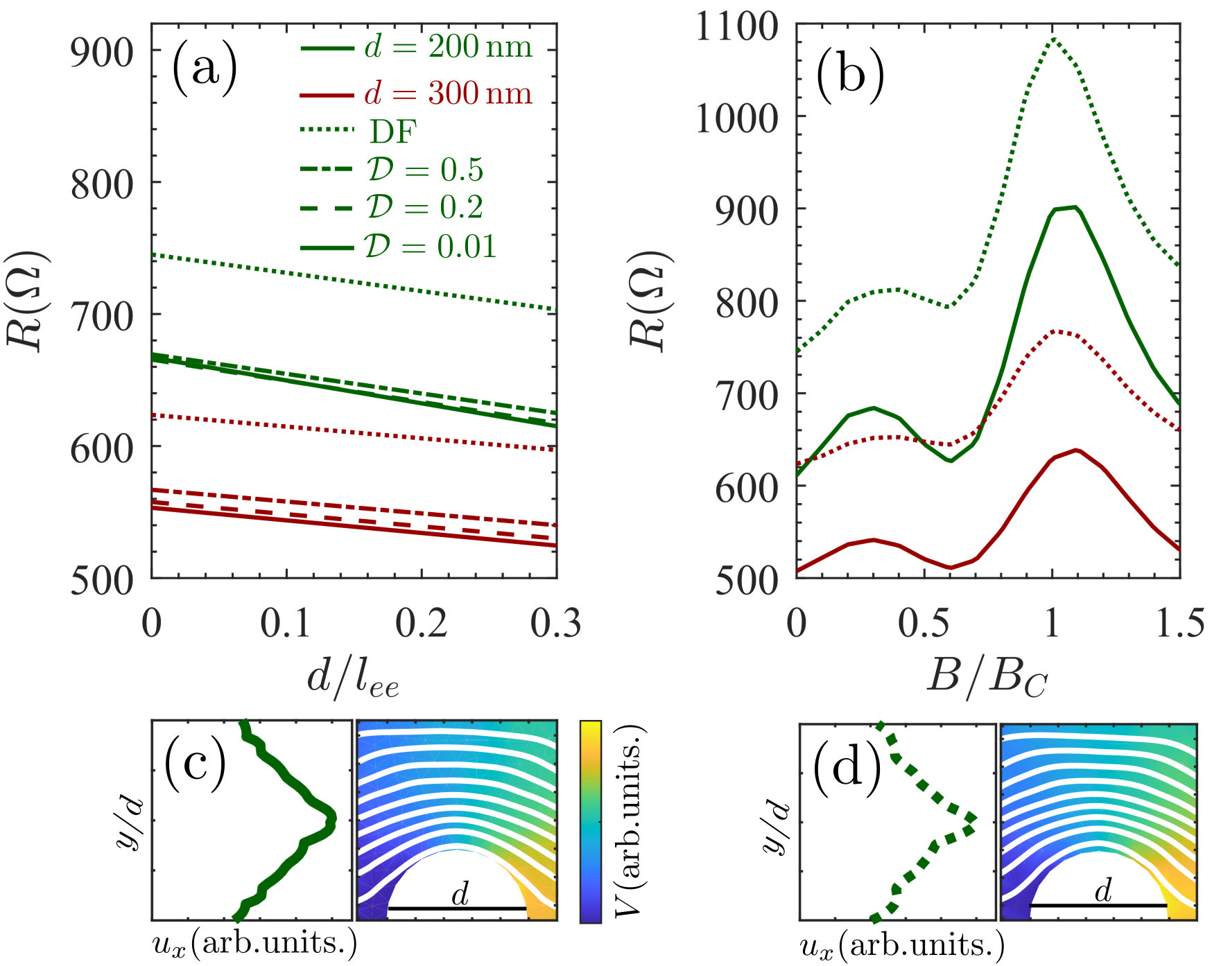
In this section, we investigate the role of edge scattering by performing simulations of the Boltzmann transport equation. Figure S7(a-b) shows the resistance as a function of the electron-electron scattering rate and the magnetic field, for several boundary conditions. The result is almost constant for several values of in a partial slip boundary condition. A perfect slip boundary condition is shown in Fig. S7(c), where the electron streamlines perfectly follow the shape of the holes. The electrical properties are not very different for the diffusive edge, whose velocity profile is shown in Fig. S7, and whose streamlines are slightly separated from the holes.
Consequently, we prove that the results are robust regardless of the edge scattering mechanism. Both the edge control of the cryo-etching technique and the fact that the electron bending is mainly controlled by the antidot geometry and not by edge scattering, ensure an almost universal viscous electron flow in our graphene devices.
Appendix I Reproducibility
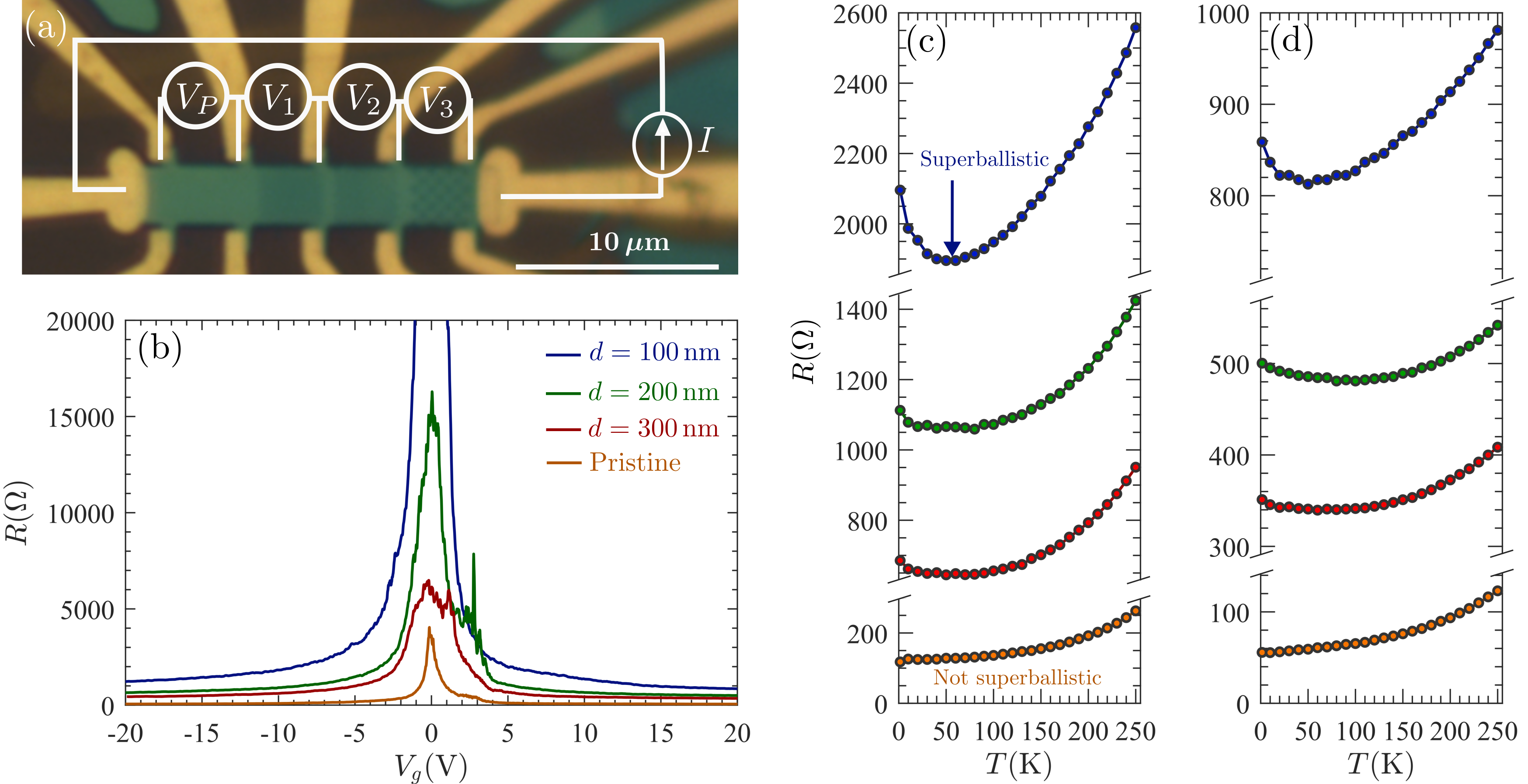
In order to further support our findings, we fabricated a second device. The new Hall bar includes the same three regions with antidots, as well as a pristine Hall-bar-like region where no antidots were defined. The experimental procedure is described in Appendix B, but now a standard 290-nm-thick SiO2 substrate was used to enable higher gate voltages without dielectric breaking. While the top hBN flake was kept comparable to the one used for the graphite back-gate sample (nm) the bottom one was significantly thinner (nm) since there was no risk of electrical short from the graphene towards an underlying metallic layer (graphite). Fig. S8(a) shows the Dirac peaks of the new sample, with the resistance as a function of the gate voltage, which is already referred to the center of the peaks. Fig. S8(b) and (c) shows the superballistic conduction in the regions with antidots, being qualitatively similar to the ones studied in Fig.2 for different densities of carriers. Most importantly no superballistic effect arise in the pristine region. In conclusion, the values of in the , and regions, further justifies the finding of superballistic conduction in antidot superlattices. Moreover, the absence of the effect in the pristine region with no antidots suggests that the geometrical engineering of the device is responsible for the superballistic conduction.
Appendix J Tomographic and hydrodynamic regimes
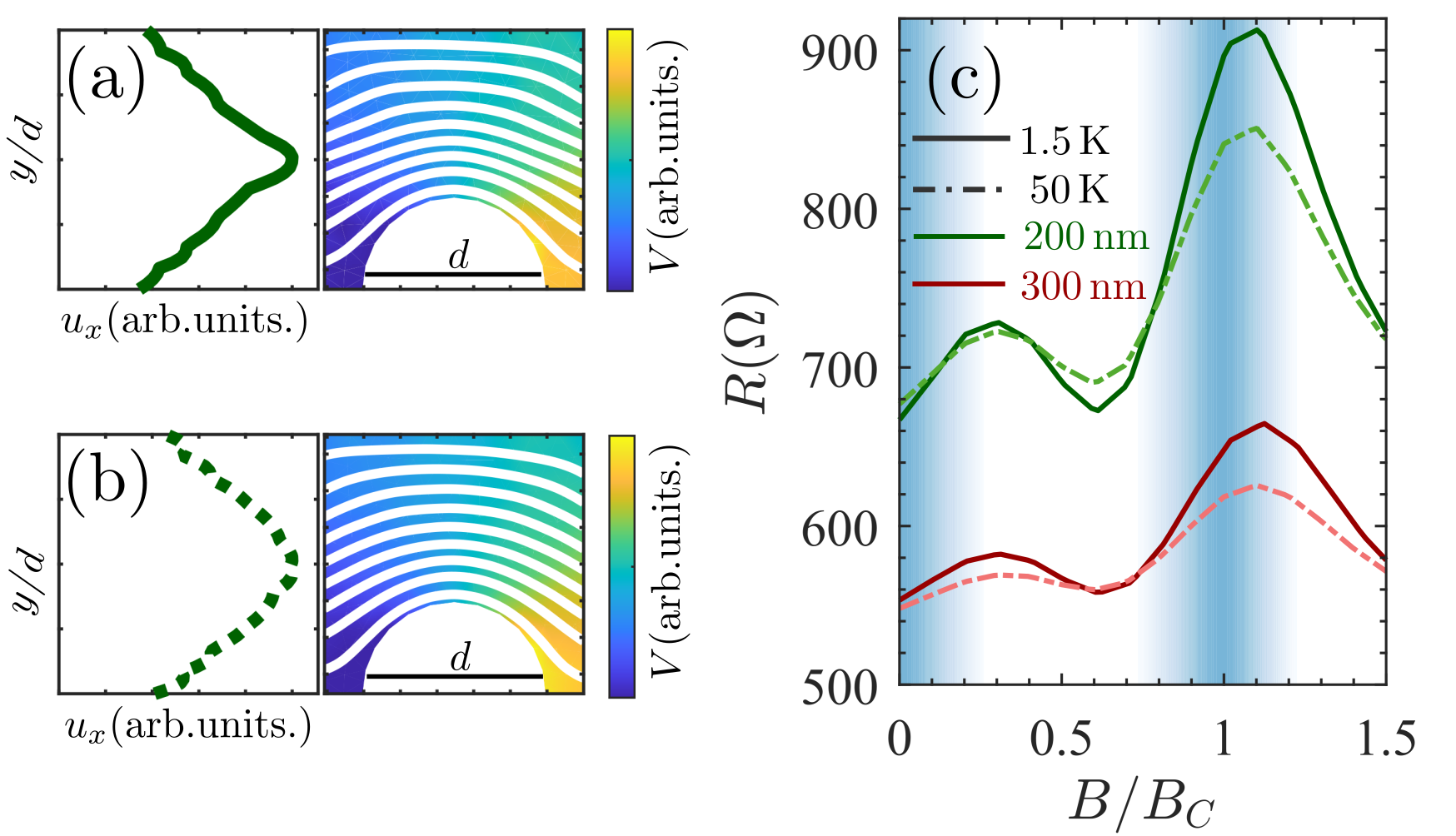
We work under the tomographic approach [35, 36], where and . Let us compare against the conventional hydrodynamic description . This comparison is possible going beyond the approximated anti-Matthiessen rule [15, 9] and solving the Boltzmann equation. Figure S9(a) and (b) shows the current distribution under both approaches. Also, Fig. S9(c) shows the magnetic response under a purely hydrodynamic description, to be compared with Fig. 3(d) for the tomographic regime. As the magnetic field increases, it rotates the velocity of the electrons and makes the distinction between even and odd parity modes less noticeable. However, the behavior is different in the absence of a magnetic field. Therefore, simulations show that there is a difference between the electrical response depending on the microscopic scattering mechanisms.
Appendix K Scaling laws
Hydrodynamic flow features properties that strongly depend on the scale. Let us analyze some relevant scaling laws affecting the device resistance in the hydrodynamic regime, . In the latter, the Boltzmann equation can be reduced to a modified Navier-Stokes equation [28] together with the continuity equation as follows
| (S6) | ||||
| (S7) |
where is the fluid drift velocity and is the viscosity. For simplicity, we write the equation in the absence of a magnetic field. Equation S7 includes a dissipative term that accounts for collisions against impurities and phonons. These equations are solved for a particular boundary condition, that in our experimental setup describes a perfectly specular edge. This imposes the no-trespassing and the perfect slip conditions, where and are the components of the velocity parallel and perpendicular to the edge.
Let us first study the physical situation such that the viscous term dominates
| (S8) |
In this case the solution for any geometrical size reads as and , where and are functions that do not depend on . Notice that these functions fulfill the perfect slip boundary condition. Furthermore, although this reasoning would not be valid for partial slip boundary conditions, it also applies to the n- slip condition commonly used for the derivation of the Poiseuille law in conventional fluids. As a consequence of the scale dependence, is the voltage drop in a region of length , and the resistance for devices of the same geometry and different sizes scales as , i.e. .
On the contrary, if the diffusive term dominates Eq. S7 reduces to
| (S9) |
which is solved by the family of solutions and . Independently of the boundary condition, this results in a constant resistance , i.e. .
In the general scenario considered in Eq. S7, there is no trivial expression for . However, we propose to make the following ansatz: . Namely, there is a single velocity field that solves both the equation with the viscous term and the dissipative term. The ansatz seems reasonable if we look at Fig. 4(d) and (e), whose streamlines are quite similar. However, the associated potentials and resistances may not be the same, so we define the bending coefficient . The latter only depends on the geometry such that a higher corresponds to a more irregular electron flow. In order to estimate we consider the total resistance in Eq. S7 as proportional to the sum of two terms (associated with the limiting cases considered in Eq. S8 and Eq. S9) that are independently simulated:
| (S10) |
As a result, we estimate for the particular geometry considered in the experiments. Last, notice that this expression is consistent with an exponent .
References
- Gurzhi [1963] R. N. Gurzhi, Minimum of resistance in impurity-free conductors, J. Exp. Theor. Phys. 17, 521 (1963).
- Gurzhi [1968] R. N. Gurzhi, Hydrodynamic effects in solids at low temperature, Sov. Phys. Usp 11, 255 (1968).
- Polini and Geim [2020] M. Polini and A. K. Geim, Viscous electron fluids, Phys. Today 73, 28 (2020).
- Narozhny [2022] B. N. Narozhny, Hydrodynamic approach to two-dimensional electron systems, Riv. del Nuovo Cim. 45, 661 (2022).
- Varnavides et al. [2023] G. Varnavides, A. Yacoby, C. Felser, and P. Narang, Charge transport and hydrodynamics in materials, Nat. Rev. Mater. 8, 726 (2023).
- Bandurin et al. [2016] D. A. Bandurin, I. Torre, R. K. Kumar, M. Ben Shalom, A. Tomadin, A. Principi, G. H. Auton, E. Khestanova, K. S. Novoselov, I. V. Grigorieva, L. A. Ponomarenko, A. K. Geim, and M. Polini, Negative local resistance caused by viscous electron backflow in graphene, Science 351, 1055 (2016).
- Bandurin et al. [2018] D. A. Bandurin, A. V. Shytov, L. S. Levitov, R. K. Kumar, A. I. Berdyugin, M. Ben Shalom, I. V. Grigorieva, A. K. Geim, and G. Falkovich, Fluidity onset in graphene, Nat. Commun. 9, 4533 (2018).
- Sulpizio et al. [2019] J. A. Sulpizio, L. Ella, A. Rozen, J. Birkbeck, D. J. Perello, D. Dutta, M. Ben-Shalom, T. Taniguchi, K. Watanabe, T. Holder, et al., Visualizing poiseuille flow of hydrodynamic electrons, Nature 576, 75 (2019).
- Krishna Kumar et al. [2017] R. Krishna Kumar, D. A. Bandurin, F. M. D. Pellegrino, Y. Cao, A. Principi, H. Guo, G. H. Auton, M. Ben Shalom, L. A. Ponomarenko, G. Falkovich, K. Watanabe, T. Taniguchi, I. Grigorieva, L. S. Levitov, M. Polini, and A. Geim, Superballistic flow of viscous electron fluid through graphene constrictions, Nat. Phys. 13, 1182 (2017).
- Kumar et al. [2022] C. Kumar, J. Birkbeck, J. A. Sulpizio, D. Perello, T. Taniguchi, K. Watanabe, O. Reuven, T. Scaffidi, A. Stern, A. K. Geim, et al., Imaging hydrodynamic electrons flowing without landauer–sharvin resistance, Nature 609, 276 (2022).
- Stern et al. [2022] A. Stern, T. Scaffidi, O. Reuven, C. Kumar, J. Birkbeck, and S. Ilani, How electron hydrodynamics can eliminate the landauer-sharvin resistance, Phys. Rev. Lett. 129, 157701 (2022).
- Nagaev and Ayvazyan [2008] K. Nagaev and O. Ayvazyan, Effects of electron-electron scattering in wide ballistic microcontacts, Phys. Rev. Lett. 101, 216807 (2008).
- Nagaev and Kostyuchenko [2010] K. Nagaev and T. Kostyuchenko, Electron-electron scattering and magnetoresistance of ballistic microcontacts, Phys. Rev. B 81, 125316 (2010).
- Renard et al. [2008] V. Renard, O. Tkachenko, V. Tkachenko, T. Ota, N. Kumada, J.-C. Portal, and Y. Hirayama, Boundary-mediated electron-electron interactions in quantum point contacts, Phys. Rev. Lett. 100, 186801 (2008).
- Guo et al. [2017] H. Guo, E. Ilseven, G. Falkovich, and L. S. Levitov, Higher-than-ballistic conduction of viscous electron flows, PNAS 114, 3068 (2017).
- Keser et al. [2021] A. C. Keser, D. Q. Wang, O. Klochan, D. Y. Ho, O. A. Tkachenko, V. A. Tkachenko, D. Culcer, S. Adam, I. Farrer, D. A. Ritchie, et al., Geometric control of universal hydrodynamic flow in a two-dimensional electron fluid, Phys. Rev. X 11, 031030 (2021).
- Poiseuille [1844] J. L. Poiseuille, Recherches expérimentales sur le mouvement des liquides dans les tubes de très-petits diamètres (Imprimerie Royale, 1844).
- Batchelor [2000] G. Batchelor, An introduction to fluid dynamics (2000).
- Landau and Lifshitz [2013] L. D. Landau and E. M. Lifshitz, Fluid mechanics: Landau And Lifshitz: course of theoretical physics, Volume 6, Vol. 6 (Elsevier, 2013).
- Gooth et al. [2018] J. Gooth, F. Menges, N. Kumar, V. Sü, C. Shekhar, Y. Sun, U. Drechsler, R. Zierold, C. Felser, and B. Gotsmann, Thermal and electrical signatures of a hydrodynamic electron fluid in tungsten diphosphide, Nat. Commun. 9, 4093 (2018).
- Baker et al. [2024] G. Baker, T. W. Branch, J. Bobowski, J. Day, D. Valentinis, M. Oudah, P. McGuinness, S. Khim, P. Surówka, Y. Maeno, et al., Nonlocal electrodynamics in ultrapure pdcoo 2, Phys. Rev. X 14, 011018 (2024).
- Aharon-Steinberg et al. [2022] A. Aharon-Steinberg, T. Völkl, A. Kaplan, A. K. Pariari, I. Roy, T. Holder, Y. Wolf, A. Y. Meltzer, Y. Myasoedov, M. E. Huber, et al., Direct observation of vortices in an electron fluid, Nature 607, 74 (2022).
- Dean et al. [2010] C. R. Dean, A. F. Young, I. Meric, C. Lee, L. Wang, S. Sorgenfrei, K. Watanabe, T. Taniguchi, P. Kim, K. L. Shepard, et al., Boron nitride substrates for high-quality graphene electronics, Nature Nanotech. 5, 722 (2010).
- Palm et al. [2024] M. L. Palm, C. Ding, W. S. Huxter, T. Taniguchi, K. Watanabe, and C. L. Degen, Observation of current whirlpools in graphene at room temperature, Science 384, 465 (2024).
- Clericò et al. [2019] V. Clericò, J. A. Delgado Notario, M. Saiz-Bretín, A. V. Malyshev, Y. M. Meziani, P. Hidalgo, B. Méndez, M. Amado, F. Domínguez-Adame, and E. Diez, Quantum nanoconstrictions fabricated by cryo-etching in encapsulated graphene, Sci. Rep. 9, 13572 (2019).
- Rhodes et al. [2019] D. Rhodes, S. H. Chae, R. Ribeiro-Palau, and J. Hone, Disorder in van der waals heterostructures of 2d materials, Nature Materials 18, 541 (2019).
- Clericò et al. [2018] V. Clericò, J. A. Delgado Notario, M. Saiz-Bretín, C. Hernández Fuentevilla, A. V. Malyshev, J. D. Lejarreta, E. Diez, and F. Domínguez-Adame, Quantized electron transport through graphene nanoconstrictions, Phys. Status Solidi A 215, 1701065 (2018).
- Estrada-Alvarez et al. [2024] J. Estrada-Alvarez, F. Dominguez-Adame, and E. Díaz, Alternative routes to electron hydrodynamics, Comm. Phys. 7 (2024).
- Holder et al. [2019] T. Holder, R. Queiroz, T. Scaffidi, N. Silberstein, A. Rozen, J. A. Sulpizio, L. Ella, S. Ilani, and A. Stern, Ballistic and hydrodynamic magnetotransport in narrow channels, Phys. Rev. B 100, 245305 (2019).
- Sandner et al. [2015] A. Sandner, T. Preis, C. Schell, P. Giudici, K. Watanabe, T. Taniguchi, D. Weiss, and J. Eroms, Ballistic transport in graphene antidot lattices, Nano Lett. 15, 8402 (2015).
- Vaquero et al. [2023] D. Vaquero, V. Clericò, M. Schmitz, J. A. Delgado-Notario, A. Martín-Ramos, J. Salvador-Sánchez, C. S. Müller, K. Rubi, K. Watanabe, T. Taniguchi, et al., Phonon-mediated room-temperature quantum hall transport in graphene, Nat. Comm. 14, 318 (2023).
- Hwang and Sarma [2008] E. Hwang and S. D. Sarma, Acoustic phonon scattering limited carrier mobility in two-dimensional extrinsic graphene, Phys. Rev. B 77, 115449 (2008).
- Giuliani and Vignale [2008] G. Giuliani and G. Vignale, Quantum theory of the electron liquid (Cambridge university press, 2008).
- Callaway [1959] J. Callaway, Model for lattice thermal conductivity at low temperatures, Phys. Rev. 113, 1046 (1959).
- Ledwith et al. [2019] P. Ledwith, H. Guo, A. Shytov, and L. Levitov, Tomographic dynamics and scale-dependent viscosity in 2d electron systems, Phys. Rev. Lett. 123, 116601 (2019).
- Kryhin et al. [2023] S. Kryhin, Q. Hong, and L. Levitov, -linear conductance in electron hydrodynamics, arXiv preprint arXiv:2310.08556 (2023).
- Kiselev and Schmalian [2019] E. I. Kiselev and J. Schmalian, Boundary conditions of viscous electron flow, Phys. Rev. B 99, 035430 (2019).
- Pezzini et al. [2012] S. Pezzini, C. Cobaleda, E. Diez, and V. Bellani, Quantum interference corrections to magnetoconductivity in graphene, Phys. Rev. B 85, 165451 (2012).
- Eroms and Weiss [2009] J. Eroms and D. Weiss, Weak localization and transport gap in graphene antidot lattices, NJP 11, 095021 (2009).
- Power et al. [2017] S. R. Power, M. R. Thomsen, A.-P. Jauho, and T. G. Pedersen, Electron trajectories and magnetotransport in nanopatterned graphene under commensurability conditions, Phys. Rev. B 96, 075425 (2017).
- Yagi et al. [2015] R. Yagi, R. Sakakibara, R. Ebisuoka, J. Onishi, K. Watanabe, T. Taniguchi, and Y. Iye, Ballistic transport in graphene antidot lattices, Phys. Rev. B 92, 195406 (2015).
- Afanasiev et al. [2021] A. Afanasiev, P. Alekseev, A. Greshnov, and M. Semina, Ballistic-hydrodynamic phase transition in flow of two-dimensional electrons, Phys. Rev. B 104, 195415 (2021).
- Di Ventra [2008] M. Di Ventra, Electrical Transport in Nanoscale Systems (Cambridge University Press, 2008).
- Whiteley [2017] J. Whiteley, Finite Element Methods, Mathematical Engineering (Springer International Publishing AG, 2017).
- Engwirda and Ivers [2016] D. Engwirda and D. Ivers, Off-centre steiner points for delaunay-refinement on curved surfaces, Computer-Aided Design 72, 157 (2016).
- Ginzburg et al. [2023] L. V. Ginzburg, Y. Wu, M. P. Röösli, P. R. Gomez, R. Garreis, C. Tong, V. Stará, C. Gold, K. Nazaryan, S. Kryhin, et al., Long distance electron-electron scattering detected with point contacts, Phys. Rev. Res. 5, 043088 (2023).