Oscillatory Bias Dependence of Visible Height of Monatomic Pb(111) Steps: Consequence of Quantum-Size Effect for Thin Metallic Films
I Abstract
Local structural and electronic properties of thin Pb(111) films grown on Si(111) surface are experimentally studied by means of low-temperature scanning tunneling microscopy and spectroscopy (STM/STS). It is shown that the visible height of the monatomic step on Pb(111) surface demonstrates oscillatory dependence on bias voltage . The period of these oscillations coincides with the period of the oscillations of both local tunneling conductance () and the rate of the STM tip displacement () at sweeping . It points to the fact that the observed oscillations of the visible height of monatomic Pb(111) step are controlled by coherent resonant tunneling of electrons from the STM tip to Pb(111) film through quantum-well states in thin Pb(111) film. We argue that the maximum and minimum visible heights of the monatomic Pb(111) step correspond to the bias voltages, at which local densities of states for the Pb(111) terraces of different thicknesses are equal.
∗ Corresponding author, e-mail address: aladyshkin@ipmras.ru
II Introduction
An appearance of discrete quantum-well states due to the confinement of electrons in low-dimensional samples is known to determine unusual thermodynamic and transport properties of solid-state nanostructures (see, e.g., textbooks Ferry-book-09 ; Nazarov-book-09 ). Indeed, for thin-film samples electrons in the conduction band can be considered as nearly free particles for motion in the lateral direction and confined for motion in the transverse direction similar to a ’particle-in-the-box’ problem. For such systems, there are localized solutions of the Schrödinger equation, which have form of standing electron waves with integer number of half-waves inside thin conducting film with exponentially decaying tails in the barrier area. Quantization of the transverse wave vector and the energy for the electronic quantum-well states apparently results in the modification of the energy spectrum. In particular, coherent resonant tunneling Ferry-book-09 through quasi-stationary quantum-well states (see schematic energy diagram in figure 1 from Ref. 3) leads to the appearance of almost equidistantly positioned peaks on the dependence of the differential tunneling conductance on the bias voltage both for filled and empty electronic states in experiments involving scanning tunneling microscopy and spectroscopy (STM/STS). Altfeder-PRL-97 ; Altfeder-PRL-98a ; Altfeder-PRL-98b ; Su-PRL-01 ; Eom-PRL-06 ; Hong-PRB-09 ; Kim-SurfSci-15 ; Ustavshchikov-JETPLett-17 ; Putilov-JETPLett-19 ; Aladyshkin-JPCC-21
Two-dimensional Pb(111) islands seem to be convenient objects for studying quantum-size effects in metallic films in normal and superconducting states by means of STM/STS Altfeder-PRL-97 ; Altfeder-PRL-98a ; Altfeder-PRL-98b ; Su-PRL-01 ; Eom-PRL-06 ; Hong-PRB-09 ; Kim-SurfSci-15 ; Ustavshchikov-JETPLett-17 ; Putilov-JETPLett-19 ; Aladyshkin-JPCC-21 and by transport and Hall measurements;Miyata-PRB-08 ; Jalochowski-PRB-88a ; Jalochowski-PRB-88b for the investigation of electronic properties in superconducting nanostructures Cren-PRL-09 ; Ning-ERL-09 and superconducting two-dimensional materials,Brun-SuST-17 hybrid structures superconductor-ferromagnet,Aladyshkin-PRB-11a ; Aladyshkin-PRB-11b ; Iavarone-NatCom-14 superconductor-normal metal,Cherkez-PRX-14 ; Roditchev-NatPhys-15 and superconductor-topological insulator;Stolyarov-JPCLett-21 and for the investigation of electronic states by means of photoemission electron spectroscopy. Mans-PRB-02 ; Dil-PRB-06 The particular sensitivity of the interference patterns to the variations of the film thickness and the crystalline structure of the interfaces makes it possible to visualize monatomic steps at the upper/lower interfaces, Altfeder-PRL-97 ; Altfeder-PRL-98a ; Altfeder-PRL-98b ; Kim-SurfSci-15 ; Ustavshchikov-JETPLett-17 atomic lattice of the substrate covered by metal, Altfeder-PRL-98a ; Altfeder-PRL-98b various inclusions, Ustavshchikov-JETPLett-17 terraces with nonquantized height variations, Putilov-JETPLett-19 and subsurface dislocation loops.Aladyshkin-JPCC-21
This paper is devoted to the experimental investigations of structural and electronic properties of thin Pb(111) films in the presence of quantum-well states. One can expect that the periodic variations of the local differential tunneling conductance for atomically flat Pb(111) terraces as a function of tunneling voltage will be converted into an oscillatory dependence of a distance between the STM tip and a sample surface during scanning process. Since the bias-induced variation of the local conductance for the terraces of the thickness differing by one monolayer occurs in out-of-phase manner (see, e.g., Refs. Ustavshchikov-JETPLett-17 ; Putilov-JETPLett-19 ), one can anticipate to detect periodic variations of the visible height of the monatomic step on the upper surface of the Pb(111) film as sweeping . To the best of our knowledge, we report on a new and reproducible effect concerning a direct experimental observation of the oscillatory dependence of the apparent height of the monatomic step between two atomically flat terraces on top of the Pb(111) island at varying tunneling voltage. We believe that this finding can be of scientific and methodological interest as a clear example of an effect of the quantum-well states on topography images of thin metallic film. We think that the effect described in our paper is rather instrumental caused by the systematic influence of quantum-well states on resulting tunneling conductance than real field-induced expansion deformation in ultrathin Pb islands in a strong electric field.Chan-PRL-12
III Methods
Experimental investigations of structural and electronic properties of quasi-two-dimensional Pb islands were carried out in an ultra-high vacuum (UHV) low-temperature scanning probe microscopy setup (Omicron Nanotechnology GmbH) operating at a base vacuum pressure mbar. Si(111) crystals were first out-gassed at about 600∘C for several hours and then cleaned in-situ by direct-current annealing at about 1300∘C, resulting in formation of reconstructed Si(111)77 surface. Thermal deposition of Pb (Alfa Aesar, purity of 99.99%) from a Mo crucible was performed in situ on Si(111)77 surface at room temperature by means of an electron-beam evaporator (Focus GmbH, model EFM3) at mbar. The orientation of the atomically flat terraces at the upper surface of the Pb islands corresponds to the (111) plane Altfeder-PRL-97 ; Su-PRL-01 ; Eom-PRL-06 . All STM/STS measurements were carried out at liquid nitrogen temperatures (from 77.4 to 80 K) with electrochemically etched W tips cleaned in situ by electron bombardment.
The topography of the Pb islands was studied by low-temperature STM by tracking the displacement of a STM tip mounted on a piezoscanner during scanning above the sample surface with active feedback loop (at constant tunneling current ) and constant electrical potential of the sample () with respect to a virtually grounded STM tip (). Hereafter we will use the following correction coefficients and for scanning tunneling measurements in the lateral and transverse directions, respectively. These factors convert nominal values , and values, recorded by a STM Control Unit (raw data), into real dimensions: , and . The procedure of fine calibration of piezoscanner is described in Supporting Information in detail. The local electronic properties of the Pb islands were studied by low-temperature STS in the regime with active feedback, constant tunneling current, and variable distance between the tip and the sample surface.Aladyshkin-JPCC-22
We would like to emphasize that the signal of the feedback loop acquired in the regime of the constant tunneling current is usually interpreted as a topography map . We demonstrate below that the signal of the feedback loop is not solely determined by sample topography, and it is influenced by the local electronic properties of a nanostructured sample.
IV Results and Discussion
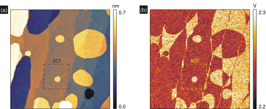
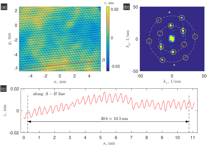
An overview topography image of the Pb(111) film with several atomically flat terraces on the upper surface is presented in figure 1a. Hereafter, we focus on local structural and electronic properties of the area (depicted by a dashed rectangle) containing two flat terraces, whose local thicknesses differ by one monolayer. Comparing the topography image (figure 1a) and the map of local differential conductance (figure 1b) recorded simultaneously at the same bias voltage, we conclude that there are no visible and hidden defects like monatomic steps in Si(111) substrate and/or inclusions inside the area of interest (AOI). It ensures that the compensation of the global tilt of the sample on the topography images both along and axes can be performed with high accuracy. As a consequence, the estimate of the visible height of monatomic Pb(111) step within such AOI seems to be the most reliable. A typical small-scale topography image demonstrates a two-dimensional hexagonal lattice for a single terrace of Pb(111) film (figure 2a).
In order to investigate experimentally the dependence of the visible height of monatomic Pb(111) step on tunneling voltage we carry a series of 24 combined topographic-spectroscopical measurements within the area of interest. Each measurement takes about 20 min and gives us the topography map and the map of the differential tunneling conductance , both acquired at the same value. Since clean surfaces of the Pb(111) film are not ideally flat and large-scale inhomogeneities are detectable (see yellow and blue regions in figure 2a and blue and dark-blue regions in figure 3a), there is a question concerning a reliable estimate of the height of the monatomic Pb(111) step. In addition, due to unavoidable thermal drift, the particular location of the upper terrace with respect to the bounds of the scanning area changes during long-term investigations (24 ’forward-and-backward’ scans within one working day). The drift makes impossible simple mathematical subtraction one topography image recorded at bias voltage from another image recorded at bias voltage to find any differences, related to the effect of bias voltage. To avoid additional instrumental complications, we consider only forward measurements.
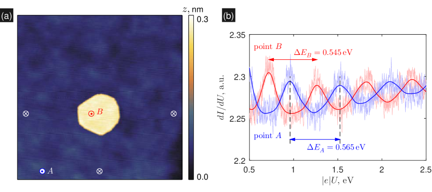
Figure 3a shows typical topography image within the area of interest. The dependences of the local differential tunneling conductance on acquired for the terraces of different thicknesses (points and ) in the regime with active feedback loop are presented in figure 3b. Pronounced periodic oscillations in the dependence on at low bias voltage (V) can be considered as clear experimental evidence for the coherent resonant tunneling through quantum-well states localized in thin metallic film Altfeder-PRL-97 ; Altfeder-PRL-98a ; Altfeder-PRL-98b ; Su-PRL-01 ; Eom-PRL-06 ; Hong-PRB-09 ; Kim-SurfSci-15 ; Ustavshchikov-JETPLett-17 ; Putilov-JETPLett-19 ; Aladyshkin-JPCC-21 . Taking the periods of the quantum-size oscillations eV and eV, one can estimate the local thickness of the Pb film with respect to the Si(111) surface using the relationships nm and nm, where cm/s is the Fermi velocity for the Pb(111) films. The theoretical estimate for the monatomic step on the Pb(111) surface is nm, where nm is the lattice constant for bulk Pb. As a consequence, the local thickness for the lower terrace in figure 3a is equal to 23 monolayers, while the local thickness for the upper terrace is equal to 24 monolayers.
In order to estimate the apparent height of the monatomic Pb(111) step we apply three different approaches.
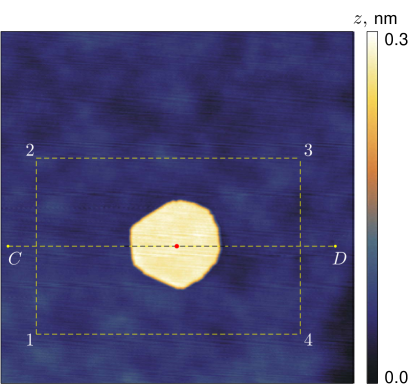
First, we manually choose a rectangular area of the same size surrounding the upper terrace for each topography image (see contour 1-2-3-4 in figure 4). Then, we compose histograms illustrating the height distribution within this area for each scan. It is obvious that the probability density function should have two maxima (figure 5a): the positions of the main and minor peaks correspond to the mean relative heights for the lower and upper terraces, respectively. The probability density function for each value can be well fitted by a superposition of two Gaussian functions
| (1) |
where , and are fitting parameters. Measuring the interval between these peaks for the series of measurements at different bias voltages, one can determine the dependence of the visible height of the monatomic Pb(111) step: on (figure 5b).
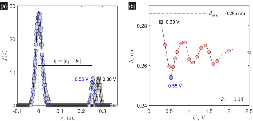
Considering data presented in figure 5, we conclude that
(i) the visible height of the monatomic Pb(111) step varies with oscillations as bias voltage monotonously increases;
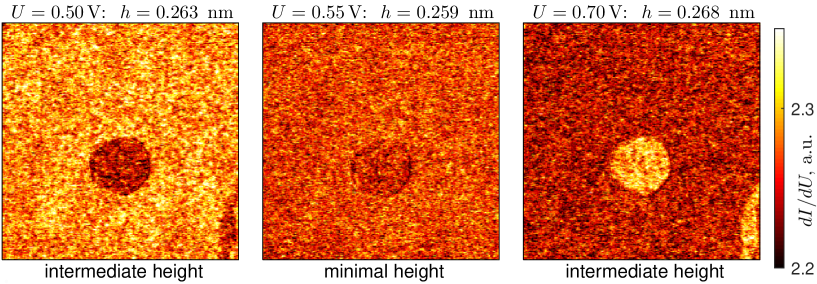
(ii) the maximal effect of the bias-induced variation of the height observed experimentally is about 0.03 nm or 10% from the theoretical limit for the Pb(111) monolayer (0.286 nm);
(iii) the detected period of the height oscillations (about 0.55 eV) is very close to the period of the variations of the differential tunneling conductance as a function of , controlled by quantum-well states in thin Pb films (figure 3a);
(iv) all values are smaller than the theoretical limit for the Pb(111) monolayer, provided we use the mean correction factor .
In order to confirm that the observed oscillatory dependence of on is not an artifact of statistical treatment, we consider alternative methods of data analysis.
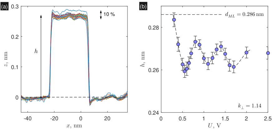
The second approach is based on a cross-sectional analysis. We find the geometrical center of the upper terrace (red point in figure 4) and then plot the cross-sectional view along the axis via the center of the terrace regardless of particular locations of this terrace with respect to bounds of a topography image for all scans. All these profiles are shown in figure 6a. The visible height of the monatomic step can be defined now as the vertical separation between the mean values for the upper terrace and for the lower terrace. It is easy to see that the mean height of the monatomic step with respect to the background level indeed depends on the bias voltage. The dependence of on shown in figure 6b expectedly coincides with the result of the histogram analysis (figure 5b).
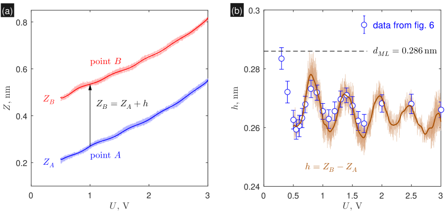
Third, we acquire a series of the local distance-voltage () spectroscopic measurements in the regime of constant tunneling current.Aladyshkin-JPCC-22 Two tunneling spectra and for the lower and upper terraces are shown in figure 7a. It is clear that the dependence of on (figure 7b) very well reproduces the results of previous analysis (see figures 5 and 6). It is important to note that measurements are rather fast (1 min per line for entire range of the considered values instead of 20 min per two-dimensional scan for a single value), therefore temperature-induced variations of both a piezocoefficient and the correction factor should be negligible (see figures S2-S4 in the Supporting Information).
Thus, based on our experimental observations, we conclude that the quantum-well states in thin Pb(111) film play a role of a systematic and reproducible inaccuracy factor affecting the STM measurements in a topographic mode. We would like to emphasize that the actual thickness of the Pb film in the area of interest is not extremely small (23-24 monolayers) and all of the measurements were performed in the limit of low-tunneling current (400 pA). This substantially differs from Ref. Chan-PRL-12 , where properties of ultrathin Pb films (from 2 to 16 monolayers) were studied in the limit of high-tunneling current (up to 50 nA) and high-tunneling voltage (up to 5 V), what a results in strong electric field near the tip apex. As a consequence, we do not consider our bias-dependent oscillatory dependence of the visible height of the Pb (111) step as an indication of the real field-induced deformations of Pb films according to Ref. Chan-PRL-12 .
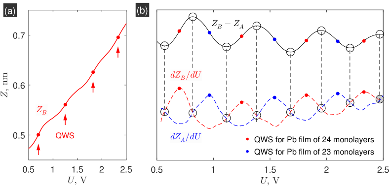
Finally, we would like to discuss the phase of the oscillations of the visible height of the Pb(111) step as a function of with respect to the and oscillations occurring in phaseAladyshkin-JPCM-20 and both controlled by resonant tunneling of electrons through quantum-well states in thin Pb(111) films. The black solid line in figure 8 shows the bias-induced variations on the visible height derived from experimental and dependences (figure 7) after the removal of high-frequency noise by additional running Gaussian averaging. Filtration of the noisy component was apparently necessary for the numerical differentiation of raw data and getting the dependences on and on (blue and red dashed lines in figure 8b, correspondingly). It is clear that the extremal values of should correspond to the values satisfying the conditions
| (2) |
It means that both maximal and minimal values of the oscillations can be observed at bias voltages, at which the rate of the tip displacement () for the Pb(111) terraces of different thickness are equal (figure 8). Since the oscillations of and as a function of occur in phase, we conclude that the maximal and minimal of the visible height of the monatomic Pb(111) step should correspond to the case of equal differential tunneling conductance for the Pb(111) terraces of different thicknesses. This conclusion is nicely supported by the results of the combined STM/STS measurements (figure 9).
V Conclusion
We experimentally studied the peculiarities of resonant tunneling through quantum-well states in thin Pb(111) films by means of low-temperature scanning tunneling microscopy and spectroscopy. All measurements were carried out in the regime constant tunneling current with an active feedback loop. We argued that the quantum-well states in Pb(111) films are responsible for the oscillatory dependence of the visible height of the monatomic Pb(111) step on the sample surface, measured by scanning tunneling microscopy, as a function of bias voltage. We experimentally demonstrated that the maximum and minimum visible heights of the monatomic Pb(111) step correspond to the bias voltages, at which there is no contrast in the differential tunneling conductance for the Pb(111) terraces of different thicknesses. We believe that such the oscillatory behavior should be a common property for all thin-film samples, provided that resonant electron tunneling via quantum-well states is not completely suppressed by thermal effects and structural imperfections.
Supporting Information
Additional figures illustrating the details of fine calibration of piezoscanner at liquid nitrogen temperatures
Acknowlednements
The author is grateful to S. I. Bozhko, S. V. Zaitsev-Zotov, A. A. Zhukov and A. V. Putilov for fruitful discussions and valuable comments. The work was performed with the use of the facilities at the Common Research Center ’Physics and Technology of Micro- and Nanostructures’ at Institute for Physics of Microstructures RAS and funded by the Russian State Contract (No. FFUF-2021-0020).
References
References
- (1) Ferry, D. K.; Goodnick, S. M. Transport in nanostructures. 2nd ed. Cambridge University Press: Cambridge, U.K., 2009.
- (2) Nazarov, Y. V.; Blanter, Y. M. Quantum Transport: Introduction to Nanoscience. Cambridge University Press: New York, USA, 2009.
- (3) Aladyshkin, A. Yu.; Schouteden K. Field-emission resonances in thin metallic films: Nonexponential decrease of the tunneling current as a function of the sample-to-tip distance. J. Phys. Chem. C 2022, 126, 13341–13348.
- (4) Altfeder, I. B.; Matveev, K. A.; Chen D. M. Electron fringes on a quantum wedge. Phys. Rev. Lett. 1997, 78, 2815-2818.
- (5) Altfeder, I. B.; Chen, D. M.; Matveev, K. A. Imaging buried interfacial lattices with quantized electrons. Phys. Rev. Lett. 1998, 80, 4895-4898.
- (6) Altfeder, I. B.; Narayanamurti, V.; Chen, D. M. Imaging subsurface reflection phase with quantized electrons. Phys. Rev. Lett. 2002, 88, 206801.
- (7) Su, W. B.; Chang, S. H.; Jian, W. B.; Chang, C. S.; Chen, L. J.; Tsong, T. T. Correlation between quantized electronic states and oscillatory thickness relaxations of 2D Pb islands on Si(111)–(77) surfaces. Phys. Rev. Lett. 2001, 86, 5116-5118.
- (8) Eom, D.; Qin, S.; Chou, M. Y.; Shih, C. K. Persistent superconductivity in ultrathin Pb films: A scanning tunneling spectroscopy study. Phys. Rev. Lett. 2006, 96, 027005.
- (9) Hong, I.; Brun, C.; Patthey, F.; Sklyadneva, I. Yu.; Zubizarreta, X.; Heid, R.; Silkin, V. M.; Echenique, P. M.; Bohnen, K. P.; Chulkov, E. V., et al. Decay mechanisms of excited electrons in quantum-well states of ultrathin Pb islands grown on Si(111): Scanning tunneling spectroscopy and theory. Phys. Rev. B 2009, 80, 081409.
- (10) Kim, J.; Qin, S.; Zhang, Y.; Zhu, W.; Shih, C.-K. Influence of quantum well states on the formation of Au-Pb alloy in ultra-thin Pb films. Surf. Sci. 2015, 632, 174-179.
- (11) Ustavshchikov, S. S.; Putilov, A. V.; Aladyshkin, A. Yu. Tunneling interferometry and measurements of thickness of ultra-thin metallic films Pb(111). JETP Lett. 2017, 106, 491-497.
- (12) Putilov, A. V.; Ustavshchikov, S. S.; Bozhko, S. I.; Aladyshkin, A. Yu. Nonuniform quantum-confined states and visualization of hidden defects in thin Pb(111) films. JETP Lett. 2019, 109, 755-761.
- (13) Aladyshkin, A. Yu.; Aladyshkina, A. S.; Bozhko, S. I. Observation of hidden parts of dislocation loops in thin Pb films by means of scanning tunneling spectroscopy. J. Phys. Chem. C 2021, 125, 26814-26822.
- (14) Miyata, N.; Horikoshi, K.; Hirahara, T.; Hasegawa, S.; Wei, C. M.; Matsuda, I. Electronic transport properties of quantum-well states in ultrathin Pb (111) films. Phys. Rev. B 2008, 78, 245405.
- (15) Jałochowski, M.; Bauer, E. Quantum size and surface effects in the electrical resistivity and high-energy electron reflectivity of ultrathin lead films. Phys. Rev. B 1988, 38, 5272-5280.
- (16) Jałochowski, M.; Hoffman, M.; Bauer, E. Quantized Hall effect in ultrathin metallic films. Phys. Rev. Lett. 1996, 76, 4227-4229.
- (17) Cren, T.; Fokin, D.; Debontridder, F.; Dubost, V.; Roditchev, D. Ultimate vortex confinement studied by scanning tunneling spectroscopy. Phys. Rev. Lett. 2009, 102, 127005.
- (18) Ning, Y. X.; Song, C. L.; Guan, Z. L.; Ma, X. C.; Chen, Xi.; Jia, J. F.; Xue, Q. K. Observation of surface superconductivity and direct vortex imaging of a Pb thin island with a scanning tunneling microscope. Europhys. Lett. 2009, 85, 27004.
- (19) Brun, C.; Cren, T.; Roditchev, D. Review of 2D superconductivity: the ultimate case of epitaxial monolayers. Supercond. Sci. Technol. 2017, 30, 013003.
- (20) Aladyshkin, A. Yu.; Fritzsche, J.; Kramer, R. B. G.; Werner, R.; Guenon, S.; Kleiner, R.; Koelle, D.; Moshchalkov, V. V. Crossover between different regimes of inhomogeneous superconductivity in planar superconductor-ferromagnet hybrids. Phys. Rev. B 2011, 84, 094523.
- (21) Werner, R.; Aladyshkin, A. Yu.; Guenon, S.; Fritzsche, J.; Nefedov, I. M.; Moshchalkov, V. V.; Kleiner, R.; Koelle, D. Domain-wall and reverse-domain superconducting states of a Pb thin-film bridge on a ferromagnetic BaFe12O19 single crystal. Phys. Rev. B 2011, 84, 020505(R).
- (22) Iavarone, M.; Moore, S. A.; Fedor, J.; Ciocys, S. T.; Karapetrov, G.; Pearson, J.; Novosad, V.; Bader, S. D. Visualizing domain-wall and reverse-domain superconductivity. Nature Commun. 2014, 5, 4766.
- (23) Cherkez, V.; Cuevas, J. C.; Brun, C.; Cren, T.; Menard, G.; Debontridder, F.; Stolyarov, V. S.; Roditchev, D. Proximity effect between two superconductors spatially resolved by scanning tunneling spectroscopy. Phys. Rev. X 2014, 4, 011033.
- (24) Roditchev, D.; Brun, C.; Serrier-Garcia, L.; Cuevas, J. C.; Bessa, V. H. L.; Milošević, M. V.; Debontridder, F.; Stolyarov, V.; Cren, T. Direct observation of Josephson vortex cores. Nature Phys. 2015, 11, 332-337.
- (25) Stolyarov, V. S.; Pons, S.; Vlaic, S.; Remizov, S. V.; Shapiro, D. S.; Brun, C.; Bozhko, S. I.; Cren, T.; Menshchikova, T. V.; Chulkov, E. V., et al., Superconducting long-range proximity effect through the atomically flat interface of a Bi2Te3 topological insulator, J. Phys. Chem. Lett. 2021, 12, 9068-9075.
- (26) Mans, A.; Dil, J. H.; Ettema, A. R. H. F.; Weitering, H. H. Quantum electronic stability and spectroscopy of ultrathin Pb films on Si(111)77. Phys. Rev. B 2002, 66, 195410.
- (27) Dil, J. H.; Kim, J. W.; Kampen, Th.; Horn, K.; Ettema, A. R. H. F. Electron localization in metallic quantum wells: Pb versus In on Si(111). Phys. Rev. B 2006, 73, 161308.
- (28) Chan, W. Y.; Huang, H. S.; Su, W. B.; Lin, W. H.; Jeng, H.-T.; Wu, M. K.; and Chang C. S. Field-induced expansion deformation in Pb islands on Cu(111): Evidence from energy shift of empty quantum-well states. Phys. Rev. Lett. 2012, 108, 146102.
- (29) Aladyshkin, A. Yu. Quantum-well and modified image-potential states in thin Pb(111) films: an estimate for the local work function. Journal of Physics: Condensed Matter 2020, 32, 435001.
Supporting Information
Oscillatory Bias Dependence of the Visible Height of Monatomic Pb(111) Steps: Consequence of the Quantum-Size Effect for Thin Metallic Films
Reconstruction Si(111) (see [S.1]-[S.3]) with well-known parameters can be considered as a test surface for the calibration of our piezoscanner at liquid nitrogen temperatures. We would like to emphasize that for the calibration purposes we use 0.5-mm thick Si(111) single crystals with clean surface without Pb layer on top. All measurements (both main and supporting) were carried out with a thin-wall piezoscanner extended at about 80 % from the maximal value after thermal stabilization (at least 3-4 hours before starting measurements).
Fine calibration of piezoscanner in the vertical direction

All and values are non-corrected dimensions (in the other words, output values recorded directly from the STM Control Unit).
Figure S1(a) shows typical topography image recorded at V and K. This image was aligned in such a way to remove global tilt both along and axes (i.e. along fast and slow scanning directions, respectively). Considering typical cross-sectional view [figure S1(b)], we estimate the visible height of the monatomic steps on the Si(111) surface: nm (with 95% confidence level). Comparing this value with the theoretical prediction for an ideal Si(111) monolayer nm (where nm is the lattice constant for bulk Si), we conclude that the dimensionless correction factor is equal to
| (S3) |
Thus, nominal output values can be converted into real dimensions by the following rule
| (S4) |
If necessary, the value can be refined using statistical analysis applied to two-dimensional images. Figure S1(c) shows the histogram, which illustrates the distribution of the visible heights for the aligned topography image in figure S1(a). The composed histogram has ten narrow peaks, corresponding to the contribution of ten atomically-flat terraces. Each of the peaks in the probability density function can be described by a Gaussian function
| (S5) |
where is the coefficient proportional to the area of the th terrace, is the mean visible height of the th terrace and is the coefficient (independent on ), which characterizes natural corrugation for the atomically-flat terrace and the accuracy of the tilt compensation. Comparing the positions of two peaks (marked by red and blue solid lines), one can independently estimate the visible height of the monatomic Si(111) step: nm (with 95% confidence level). This two-dimensional statistical analysis gives us the better estimate for the correction factor
| (S6) |
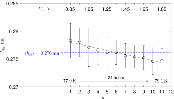
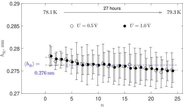
In order to check whether variations of tunneling voltage and/or unavoidable heating of both sample/piezoscanner during long-term measurements critically affect the correction factor , we perform independent series of the topographic measurements for the fixed area of clean Si(111) surface. The results of the estimates of the uncorrected visible height of the monatomic Si(111) step by means of the histogram analysis (similar to that shown in figure S1(c)) are presented in figure S2. One can see that the mean visible height monotonously decreases at 1.3% during 27-hour measurements (from 0.278 to 0.274 nm). The absence of bias-induced oscillations of for bulk sample points to that the oscillatory dependence for the visible height of the Pb(111) step described in the main paper is inherent only to thin-film samples. We think that an almost linearly decreasing dependence of on tunneling voltage should be considered as a false correlation, since the bias voltage is applied directly to the STM tip and therefore it cannot affect the properties of the piezoscanner provided that parasitic cross-talk between measurement sample-tip circuit and feedback loop is absent.
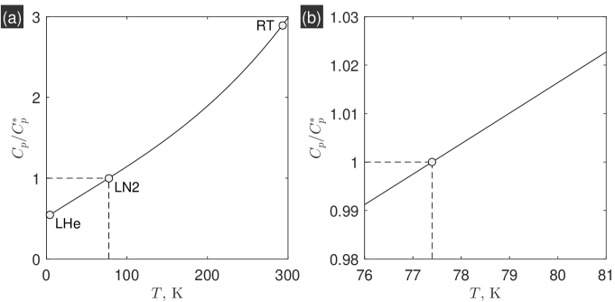
To confirm that the observed monotonously decreasing dependence of on unambiguously relates to a temperature rise, we measure a temporal dependence of for the given bias values (figure S3). During such 27-hour measurements the temperature of the sample was increased at 1.2 K (from 78.1 to 79.3 K), resulting in a decrease of at 1.5% (from 0.279 to 0.275 nm) regardless on the tunneling voltage. The described tendency (figures S2 and S3) is in qualitative and quantitative agreement with typical temperature dependence of piezo coefficient (figure S4). Indeed, the increase in temperature of the piezoscanner at 1 K leads to the increase in the piezo coefficient at about 0.7% (see [S.4]-[S.5]); therefore, the feedback loop should generate high voltage, applied to the piezoscanner, at 0.7% smaller in order to get the same displacement of the STM tip. It is worth noting that the temperature of the piezoscanner may differ from the recorded temperature assigned to the sample.
The monotonous dependence of on the sequence number of measurement can be transformed into a monotonous dependence of the correction factor on temperature. For sake of simplicity we estimate the mean correction factor taking into account temperature variations
| (S7) |
for entire range of tunneling voltages and temperatures considered in the main paper (see figures 5 and 6 of the main paper). The monotonous dependence of on (figure S3) confirms that the detected oscillatory dependence of the visible height of the monatomic Pb(111) step on the bias voltage cannot be an artifact of the measurement systems.
Fine calibration of piezoscanner in the lateral direction
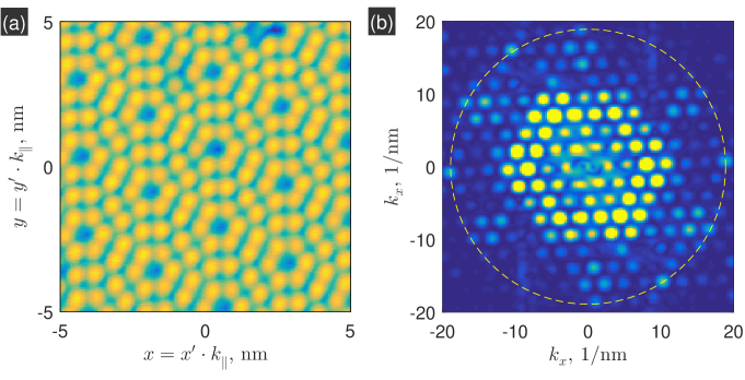
The same reconstruction Si(111) with pronounced two-dimensional periodicity can be used to find a mean correction factor for scanning tunneling measurements in the lateral direction (figure S5). This helps us to convert nominal values and , recorded by the STM Control Unit, into real dimensions
| (S8) |
References
-
[S.1]
Takayanagi, K.; Tanishiro, Y.; Takahashi, S.; Takahashi M. Structure analysis of Si(111) reconstructed surface by transmission electron diffraction. Surface Science. 1985, vol. 164, p. 367-392.
-
[S.2]
Tong, S. Y.; Huang, H.; Wei, C. M.; Packard, W. E.; Men, F. K.; Glander, G.; Webb M. B. Low-energy electron diffraction analysis of the Si(111)77 structure. Journal of Vacuum Science and Technology A. 1988, vol. 6, p. 615–624.
-
[S.3]
Oura, K.; Lifshits, V. G.; Saranin, A. A.; Zotov, A. V.; Katayama M. Surface Science: An Introduction. Springer-Verlag Berlin Heidelberg New York, 2003; Springer Science & Business Media, 2013.
-
[S.4]
The LT STM User’s Guide (including LT STM-QPlus AFM). Omicron Nanotechnology GmbH. Version 3.4, 2011.
-
[S.5]
Vandervoort, K. G.; Zasadzinski, R. K.; Galicia, G. G.; Crabtree, G. W. Full temperature calibration from 4 to 300 K of the voltage response of piezoelectric tube scanner PZT-5A for use in scanning tunneling microscopes. Review of Scientific Instruments. 1993, vol. 64, 896–899.