Strong Charge-Photon Coupling in Planar Germanium
Enabled by Granular Aluminium Superinductors
Abstract
High kinetic inductance superconductors are gaining increasing interest for the realisation of qubits, amplifiers and detectors. Moreover, thanks to their high impedance, quantum buses made of such materials enable large zero-point fluctuations of the voltage, boosting the coupling rates to spin and charge qubits. However, fully exploiting the potential of disordered or granular superconductors is challenging, as their inductance and, therefore, impedance at high values are difficult to control. Here we have integrated a granular aluminium resonator, having a characteristic impedance exceeding the resistance quantum, with a germanium double quantum dot and demonstrate strong charge-photon coupling with a rate of . This was achieved due to the realisation of a wireless ohmmeter, which allows in situ measurements during film deposition and, therefore, control of the kinetic inductance of granular aluminium films. Reproducible fabrication of circuits with impedances (inductances) exceeding ( per square) is now possible. This broadly applicable method opens the path for novel qubits and high-fidelity, long-distance two-qubit gates.
I Introduction
Superconducting circuits made from disordered superconductors with large kinetic inductance are attracting attention for the development of qubits, such as fluxonium [1, 2, 3, 4, 5], parametric amplifiers [6, 7, 8] and kinetic inductance detectors [9, 10, 11, 12, 13, 14]. High characteristic impedance devices, enabled by large kinetic inductors, are also paramount to semiconductor quantum dot qubit applications, whereby several studies have demonstrated strong charge-photon [15, 16, 17, 18] and spin-photon coupling [19, 20, 21, 22]. Furthermore, the first long-distance coherent coupling experiments between spin qubits have been reported [23, 24], leading to the first photon-mediated long-distance two-qubit gate for electron spins in Si [25]. Currently, one of the main challenges for achieving high-fidelity long-distance two-qubit gates lies in increasing the spin-photon coupling strength [25]. This can be achieved by enhancing the charge-photon coupling and the spin-orbit interaction.
The charge-photon coupling strength is enhanced with high-impedance resonators, as [26, 3, 27, 28, 29, 30]. To date, quantum dot circuit quantum electrodynamics (cQED) implementations utilising disordered nitride [31, 25, 21, 22] or Josephson junction array [17, 18] resonators have not exceeded the characteristic impedance of (Extented Fig. LABEL:fig:fige6). Outside the field of hybrid devices, much higher impedance has been achieved, either relying on the combination of a large kinetic inductance with a low stray capacitance of a suspended Josephson junction array with an impedance of > [32], or a large mutual geometric inductance with a low stray capacitance of a suspended planar coil with [33]. These approaches cannot be readily implemented with standard semiconductor spin qubits devices because of incompatibility with magnetic fields and complex nanofabrication requirements. Other studies have focused on the combination of a kinetic and mutual geometric inductance of meandered structures of thin-film TiN, with a kinetic inductance of per square () [34], or granular aluminium (grAl) with [3], both with . While grAl offers magnetic field resilience [35], lift-off compatibility [1], low losses [36], and sheet kinetic inductance reaching [37, 38, 39], it was not yet exploited for quantum dot devices. This is presumably because of the poor reproducibility of high-impedance films [40], as the film resistance, which determines the kinetic inductance, is sensitive to evaporation parameters.
In this work, we developed a high-vacuum-compatible wireless ohmmeter with an independently controlled rotary shutter, allowing for in situ measurements of the sheet resistance of the deposited film. This method allows us to reliably realise superconducting coplanar waveguide (CPW) grAl resonators with impedance exceeding , even reaching , thanks to the large sheet kinetic inductance up to . These resonators offer magnetic field resilience of and .
We integrate a grAl CPW resonator with a double quantum dot (DQD) device fabricated on a planar Ge/SiGe heterostructure confining holes, whose large spin-orbit interaction enables fast and all-electric control of spin qubits [41]. By using a resonator with a characteristic impedance of and sheet kinetic inductance of , we demonstrate a strong hole-photon coupling with a rate of and cooperativity of .
II Granular Aluminium
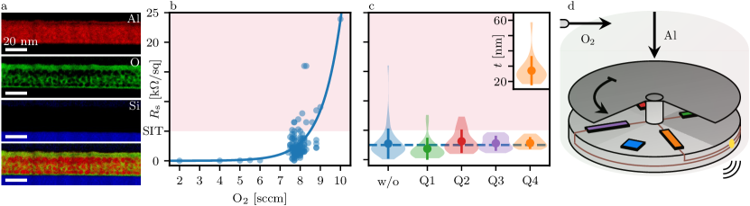
Granular aluminium has been studied for almost 60 years [42, 43] but has recently attracted increased attention as a material of interest for qubits, amplifiers and detectors [38, 1]. It consists of small crystalline grains of in diameter (Fig. 1a, red and Extented Fig. LABEL:fig:fige1) embedded in an amorphous aluminium oxide matrix (Fig. 1a, green). The aluminium grains separated by an insulating barrier can be modelled as a network of Josephson junctions, resulting in high kinetic inductance [38]. The kinetic inductance of superconductors arises from the inertia of moving Cooper pairs and increases with normal state resistance. However, it cannot be increased infinitely; it is upper-bound by a superconducting-to-insulator phase transition (SIT). For grAl films thin, the SIT has been measured around [44].
We prepare grAl by room temperature electron-beam evaporation of aluminium in an oxygen atmosphere at pressure at a rate of . The resulting resistivity of the evaporated film depends on the oxygen flow and the evaporation rate. To determine the sheet resistance, we initially used a glass sample of 10 squares and measured its resistance using a multimeter after the evaporation. The outcome of these evaporations is summarized in Fig. 1b. It is observed that the sheet resistance exponentially depends on the oxygen flow for a given evaporation rate and is not reproducible. The poor reproducibility is quantified in the blue points plot in Fig. 1c, which shows individual evaporations of resonators and cQED samples targeting . Given the poor reproducibility even for nominally identical consecutive evaporations, it is challenging to systematically fabricate high-impedance CPW resonators which operate within the designed range.
To overcome this experimental difficulty, a hermetically sealed high-vacuum compatible wireless ohmmeter has been developed (Methods and Extented Fig. LABEL:fig:fige2). It allows the in situ two-probe electrical measurement of the growing film resistance and wireless transmission of the data. This enables the termination of the evaporation when the desired value is reached. Such a procedure yields a reproducible resistance at the expense of the uncertainty in the final film thickness. This can be decreased by equipping the ohmmeter with an independent rotary shutter, as shown in Fig. 1d. It masks three-quarters of the sample holder and is wirelessly controlled. In this manner, three test samples are evaporated before the sample of interest without having to break vacuum, thus allowing the operator to fine-tune the oxygen flow and reach the desired film properties. As shown in Fig. 1c, this procedure significantly reduces the uncertainty of both resistance and thickness, making it possible to target the desired resonance frequency range. These results demonstrate a successful implementation of our technical solution, which is also transferable to other disordered superconductors and, in general, thin-film systems.
III Granular aluminium resonators
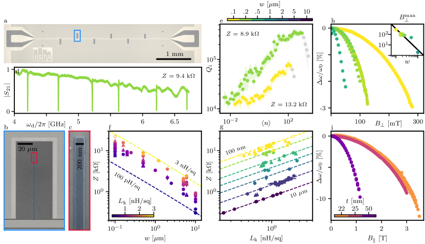
We utilize the developed method to realize high-impedance grAl CPW resonators. We first test the resonators on bare silicon () substrates. We intentionally choose low resistivity substrates as those resonators are developed for use with semiconductor heterostructures with much higher losses than highly resistive silicon or sapphire wafers [46, 27, 47]. The ground plane and feedline are comprised on Nb, with negligable kinetic inductance (Methods) and employ different CPW geometries. The hanger geometry (Fig. 2a) is preferred since it allows testing multiple resonators per chip, as well as the precise determination of internal losses and coupling rates. Figure 2b shows a scanning electron microscope image of a single grAl resonator side-coupled to a common Nb feedline. Two strategies are employed in order to maximise the impedance: first, increasing the kinetic inductance via the sheet resistance and, second, decreasing the width of the center conductor from to . Additionally, such narrow resonators exhibit an increased out-of-plane magnetic field resilience [26], beneficial for materials with low in-plane -factors [41].
In Figs. 2f, g we summarise the characteristic impedances of the fabricated resonators. Leveraging the developed wireless ohmmeter holder, we reproducibly target sheet resistances of and obtain films with a kinetic inductance reaching . The impedance scales with the kinetic inductance and the center conductor width according to
| (1) |
with () the inductance (capacitance) per length. For a superconducting resonator, the inductance per length is composed of a geometric and a kinetic contribution (Methods). The highest impedance is reached for widths below . However, we observe a limitation with three -wide samples, with most devices failing to respond to microwave excitation. These samples are highlighted with empty circles in Figs. 2f, g. The highest characteristic impedance observed for such a sample is . Nevertheless, other -wide samples demonstrate reliable performance. Specifically, five samples comprising 20 resonators with impedance ranging from to show a yield. These results demonstrate that the impedance of the grAl CPW resonators can reproducibly exceed , strongly enhancing quantum fluctuations of the voltage.
We next measure the complex frequency response with respect to the driving power and evaluate the quality factors as a function of the photon number (Methods). Fig. 2e displays a power sweep of two resonators with widths of and . The resonators retain a high-quality factor above 104 in the single photon regime, even with impedance exceeding . We conclude that high impedance grAl resonators exhibit losses that would not limit potential cQED experiments, with loss rates in the order of , which is comparable with the state-of-the-art charge/spin qubits decoherence rates [15].
To evaluate the potential of the developed CPW resonators for spin-photon coupling experiments, we investigate their magnetic field behaviour. Since the -factor of holes is highly anisotropic, with rather small in-plane and large out-of-plane -factors [48], we probe their behaviour for both magnetic field directions. In Fig. 2h, i, the relative frequency shift and the internal quality factors as a function of the applied magnetic fields for resonators with hundreds of photons are plotted. The superconducting depairing parabolically lowers the resonance frequency due to increased kinetic inductance, stemming from the decreasing superconducting gap. Furthemore, the magnetic field induces losses by introducing Abrikosov vortices in the film, whose dynamics contribute to microwave losses and resonator instability. The creation of vortices is suppressed with narrow center conductors. Thus, the maximal out-of-plane field the resonators withstand before the deterioration increases with decreasing widths, and it approximately follows [49], where is the superconducting flux quantum and is the dimension perpendicular to the applied field (inset Fig. 2g). We note that for -wide resonators, the magnetic field resilience reaches out-of-plane. Moreover, since the creation of vortices is also suppressed with thin films in the in-plane field, resonators with thickness below withstand , the thinnest reaching .
In the context of spin qubits, the demonstrated combination of high impedance and magnetic field resilience makes grAl a strong candidate for a long-range coherent coupler. For silicon-based spin qubits (-factor of 2), the spin transition can be easily brought to the range where microwave resonators are routinely operated. Moreover, such magnetic field resilience allows one to readily implement grAl resonators with spin qubits hosted in materials with highly anisotropic -factors, such as Ge. In this case, the spin qubit could be operated in an arbitrary magnetic field orientation, an important feature of operating the qubit in the parameter range where its coherence is maximized [50].
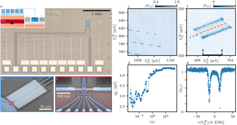
IV Strong charge-photon coupling
The strong coupling condition requires that the coherent coupling strength exceeds both the charge () and the resonator () decay rates. To coherently couple a charge with a photon, we integrate a grAl resonator with a DQD formed in a Ge/SiGe heterostructure [51] (Figs. 3a to c). We opted for a reflection geometry, which improves the signal-to-noise by a factor of two relative to the hanger geometry, where the signal can leak back to the input port [52]. The resonance frequency is measured to be , yielding a characteristic impedance of and sheet kinetic inductance of . The resonator is designed to be over-coupled, so the coupling quality factor is while the internal quality factor is ith average photons in the resonator, leading to the resonator field decay rate of . The quality factors are significantly smaller compared to a bare resonator. As described in Ref. [47], low-impedance resonators fabricated on Ge-rich substrates featuring etched quantum wells exhibit reduced internal quality factors of 104 in the single photon regime [47]. Moreover, the metallic gates for defining the quantum dots will cause significant microwave leakage, even more pronounced for high characteristic impedance [27].
The triple quantum dot array is operated as a DQD formed on the right side, with the two left-most gates grounded. The DQD is first tuned by measuring a DC current. As observed in the stability diagram in Fig. 3e, the resonator is dispersively shifted at the interdot transitions, i.e. when the DQD dipole moment becomes sizeable, allowing for direct microwave readout of individual interdot transitions (Fig. 3f). Line cuts along the right gate voltage translated to detuning through lever arms (Extented Fig. LABEL:fig:fige3 and the Methods) exhibit a sharp response in the complex resonator signal due to the interaction with the DQD. The clear dispersive interaction between the DQD and the resonator already hints towards a significant charge-photon interaction strength. However, this type of measurement does not provide sufficient information to extract the system parameters reliably [53].
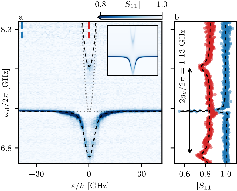
In contrast, sweeping the drive frequency while stepping the DQD detuning reveals the spectrum of the hybridized states (Fig. 4a), allowing for accurate characterization of the system. Thus, for a different interdot transition, we probe the system by reflection spectroscopy. A parabolic spectrum is expected for a DQD occupied with an odd number of holes. A clear avoided crossing is observed when the parabolic DQD charge transition frequency equals the frequency of the resonator (), as seen in Fig. 4a. Since the strong coupling condition is met, two well-resolved dressed states separated by emerge. The resonant vacuum Rabi splitting is observed (Fig. 4b), which constitutes the experimental evidence of the strong coupling regime. From Fig. 4b we extract of , with of , demonstrating strong charge-photon coupling with a cooperativity of [54]. The coupling strength agrees with the expected value with being the elementary charge, given a differential lever arm , and .
V Discussion and outlook
We have developed a wireless ohmmeter which enables us to in situ define the sheet resistance of grAl CPWs, allowing for reproducible fabrication of grAl resonators with characteristic impedance exceeding , even reaching . The reported values are more than four times higher than the state-of-the-art for semiconductor circuit quantum electrodynamics experiments [17].
Furthermore, we have shown that grAl resonators remain low-loss and are resilient to magnetic field up to in-plane and out-of-plane. By integrating a grAl resonator with a DQD formed in planar Ge we demonstrate strong hole-photon coupling with a rate of . The demonstrated charge-photon coupling strength and magnetic field resilience of the grAl resonators combined with the strong spin-orbit coupling opens the path towards strong spin-photon coupling in planar Ge [41]. Even for modest spin-orbit interaction, similar to that created by a gradient magnetic field of a micromagnet employed in Si [23, 24], spin-photon coupling rates could exceed . Such high rates suggest that two-qubit operations between distant hole spins with high fidelities are within reach [55, 56, 25].
In conclusion, we have proposed controllably deposited grAl as an alternative to Josephson junction arrays and atomically disordered superconductors for semiconductor-superconductor circuit quantum electrodynamics experiments. Its key advantages lie in being high impedance, magnetic field resilient, lift-off compatible and low-loss. By further optimising the design to reach and using an impedance of , charge-photon coupling strengths above are within reach. Moreover, the impedance can be increased beyond these values by meandering the grAl resonator and utilizing the mutual geometric inductance [34, 3]. Given the state-of-the-art quantum dot technologies and using a grAl resonator ceteris paribus, spin-photon coupling could enter the ultra-strong coupling regime, following in the footsteps of the superconducting qubits and opening an avenue towards unexplored physics [57] and advanced quantum information processing applications.
Methods
Vacuum-compatible wireless ohmmeter
The wireless ohmmeter was designed to fit the MEB550S Plassys HV electron-beam evaporator, equipped with a motorized evaporation stage. The stage can tilt between the loading and evaporation positions and rotate along the evaporation axis to ensure a uniform distribution of the deposited thin film. The ohmmeter was designed to communicate wirelessly with the handheld device outside the vacuum chamber so as not to restrict the movement of the rotary stage. The designed device uses the surface of the ohmmeter enclosure lid as a mounting surface for the samples and measuring probes. The ohmmeter circuit is placed inside the hermetically sealed enclosure, and the measuring electrodes are connected to the ohmmeter through hermetically sealed electrical cable feedthroughs. The wireless in situ resistance measurement enables the user to monitor the sheet resistance of the deposited film and to interrupt the process when the desired resistance is reached.
An independently controlled rotary shutter is magnetically coupled to a servo motor enclosed inside the holder, as magnetic coupling is a straightforward method for transferring motion from a vacuum-non-compatible motor to the high vacuum side.
The battery-powered wireless ohmmeter includes components to precisely measure the growing thin film resistance and transmit the measured values to the recording device outside the vacuum chamber. The design is based on the ATmega2560 microcontroller to communicate with the rest of the components, which include a 2.4GHz wireless transceiver, a barometer to record the temperature and pressure inside the hermetic enclosure for detecting potential pressure leaks, a servo motor to move the magnetically coupled shutter, and a precision analog-to-digital converter to measure resistance using the constant voltage method. The highest sensitivity is achieved by setting the range resistor closest to the measured value. Since the resistance of the deposited grAl spans several orders of magnitude, we use a set of four different resistors selected by switching mechanical relays to cover a large measurement range.
Sample fabrication
The bare resonators are fabricated on silicon substrates (). First, 5/ Cr/Au alignment markers are patterned using electron beam lithography (EBL), high-vacuum (HV) electron beam (e-beam) evaporation and lift-off process. Next, a Nb feedline and ground plane are defined using EBL, ultra-high vacuum (UHV) e-beam evaporation and lift-off. The grAl is not employed in this layer since achieving matching with a kinetic inductance of would require a -wide feedline separated from the ground plane by . Finally, the grAl center conductors are patterned with EBL, HV e-beam evaporation in an oxygen atmosphere and lift-off. After the evaporation, the film is subject to a static post-oxidation.
The hybrid cQED devices are fabricated on a Ge/SiGe heterostructure grown by low-energy plasma-enhanced chemical vapour deposition with forward grading [51]. The two-dimensional hole gas is self-accumulated in the Ge quantum well below the surface.
The process is as follows: First, the ohmic contacts are patterned with EBL. Before the deposition of of Pt at an angle of , a few nanometres of native oxide and SiGe spacer are removed by argon bombardment. Next, the hole gas is dry-etched with SF6-O2-CHF3 reactive ion etching everywhere except a small high mesa area extending to two bonding pads to form a conductive channel. Subsequently, the native SiO2 is removed by a dip in buffered HF before the gate oxide is deposited. The oxide is a atomic-layer-deposited aluminium oxide (Al2O3) film grown at . Next, a Nb feedline and ground plane are fabricated with EBL, UHV evaporation and lift-off. The separation of the grAl center conductor from the Nb ground plane is for resonators with a width less than . Further retraction of the ground plane would not increase the impedance appreciably. The single-layer top gates for defining the QDs are patterned in three different steps of EBL, evaporation and lift-off. The barrier and plunger gates are defined separately close to the edge of the mesa with Ti/Pd 3/. An additional Ti/Pd 3/-thick gate metal layer defines microwave filters and the bonding pads, connects to the previously defined gates and overcomes the slanted mesa edge. Finally, the grAl center conductors are defined as in the bare resonator samples.
Measurement setup
The reported low-temperature measurements were performed in a cryogen-free dilution refrigerator with a base temperature of . The sample was mounted on a custom-printed circuit board thermally anchored to the mixing chamber of the cryostat. The electrical connections were made via wire bonding. The schematic of the measurement setup is shown in Extented Fig. LABEL:fig:fige5.
Impedance evaluation
Since the characteristic impedance cannot be measured directly, we extract it from the resonance frequency. and in Eq. 1 are solely given by the design parameters (the center conductor width , the separation between the ground plane and the center conductor and the relative permittivity of the substrate ) and can be analytically calculated. We extract the characteristic impedance from the resonance frequency, which is given as
| (2) |
where and are lumped-element equivalents of the distributed parameters of the resonator. For longer, lower-impedance resonators, the coupling capacitance is usually dominated by and can be neglected. In the case of our compact high-impedance, they are of the same order of magnitude, and both have to be considered. We simulate the coupling capacitance using COMSOL electrostatic simulations. We measure the complex frequency response of a resonator and fit the signal to evaluate the resonance frequency. We calculate the sheet kinetic inductance by numerically solving Eq. 2 with the simulated coupling capacitance.
Fitting
The Heisenberg-Langevin equation of motion for a bare hanger resonator in the rotating frame is
| (3) |
where is the resonator field and is the input field. For the steady state (), it becomes
| (4) |
Using the input-output relation , where is the output field, yields the complex transmission of a bare hanger-type resonator
| (5) |
with an inserted term accounting for the impedance mismatch. Before fitting, the feedline transmission S21 is first normalized by a background trace to remove the standing wave pattern obtained from a scan with a shifted resonance frequency, either due to a magnetic field or a DQD-induced dispersive shift. The average intraresonator photon number at resonance was calculated as
| (6) |
where is the drive power after accounting for input attenuation. In the case of a single port resonator, Eq. 6 gains an extra factor of two.
For a DQD occupied with an odd number of holes, the cavity-DQD Hamiltonian in the rotating frame and rotating wave approximation can be described by
| (7) |
where is the drive frequency, is the resonance frequency, is the charge transition frequency with being the DQD detuning and the tunnel coupling. is the effective charge-photon coupling strength, () is the photon creation (annihilation) operator and is the Pauli matrix and () is the qubit lowering (raising) operator.
The Heisenberg-Langevin equations of motion for a system described by Eq. 7 are [58]
| (8) | ||||
| (9) |
For the steady state (), Eq. 9 becomes
| (10) |
which inserted in Eq. 8 with gives
| (11) |
Using yields the complex reflection of a single-port resonator coupled to a DQD charge transition
| (12) |
The translation between the gate voltages and DQD detuning is given by [59]
| (13) |
where the lever arms are extracted from bias triangles of the DQD, shown in Extented Fig. LABEL:fig:fige3.
Data Availability
All data included in this work will be available at the Institute of Science and Technology Austria repository.
Acknowledgements
We acknowledge Franco De Palma, Mahya Khorramshahi, Fabian Oppliger, Thomas Reisinger, Pasquale Scarlino and Xiao Xue for helpful discussions. This research was supported by the Scientific Service Units of ISTA through resources provided by the MIBA Machine Shop and the Nanofabrication facility. This research and related results were made possible with the support of the NOMIS Foundation, the HORIZON-RIA 101069515 project, the FWF Projects with DOI:10.55776/P32235, DOI:10.55776/I5060 and DOI:10.55776/P36507. IMP acknowledges funding from the Deutsche Forschungsgemeinschaft (DFG – German Research Foundation) under project number 450396347 (GeHoldeQED). ICN2 acknowledges funding from Generalitat de Catalunya 2021SGR00457. We acknowledge support from CSIC Interdisciplinary Thematic Platform (PTI+) on Quantum Technologies (PTI-QTEP+). This research work has been funded by the European Commission – NextGenerationEU (Regulation EU 2020/2094), through CSIC’s Quantum Technologies Platform (QTEP). ICN2 is supported by the Severo Ochoa program from Spanish MCIN/AEI (Grant No.: CEX2021-001214-S) and is funded by the CERCA Programme/Generalitat de Catalunya. Part of the present work has been performed in the framework of Universitat Autònoma de Barcelona Materials Science PhD program. AGM has received funding from Grant RYC2021-033479-I funded by MCIN/AEI/10.13039/501100011033 and by European Union NextGenerationEU/PRTR. M.B. acknowledges support from SUR Generalitat de Catalunya and the EU Social Fund; project ref. 2020 FI 00103. The authors acknowledge the use of instrumentation and the technical advice provided by the Joint Electron Microscopy Center at ALBA (JEMCA). ICN2 acknowledges funding from Grant IU16-014206 (METCAM-FIB) funded by the European Union through the European Regional Development Fund (ERDF), with the support of the Ministry of Research and Universities, Generalitat de Catalunya. ICN2 is a founding member of e-DREAM [60].
Author contribution
M.J. developed the fabrication recipes, designed the resonator and hybrid cQED devices and analysed data. K.R. developed and characterized the grAl evaporation process for the wireless ohmmeter with the help of M.J.. M.J., K.R. and C.B.E. fabricated samples and performed experiments. A.B. and T.A. conceived, designed and built the wireless ohmmeter. M.J. and O.S. developed the microwave technology for the Ge/SiGe heterostructures. S.C., D.C. and G.I. designed and grew the Ge/SiGe heterostructure. M.B., A.G.M. and J.A. performed the atomic resolution scanning transmission electron microscopy structural and electron energy-loss spectroscopy compositional-related characterization. M.J., K.R. and G.K. contributed to discussions and the preparation of the manuscript with input from the rest of the authors. G.K. and I.P. initiated, and G.K. supervised the project.
Competing interests
The authors declare no competing interests.
References
- Grünhaupt et al. [2019] L. Grünhaupt, M. Spiecker, D. Gusenkova, N. Maleeva, S. T. Skacel, I. Takmakov, F. Valenti, P. Winkel, H. Rotzinger, W. Wernsdorfer, et al., Granular aluminium as a superconducting material for high-impedance quantum circuits, Nature materials 18, 816 (2019).
- Hazard et al. [2019] T. Hazard, A. Gyenis, A. Di Paolo, A. Asfaw, S. Lyon, A. Blais, and A. Houck, Nanowire superinductance fluxonium qubit, Physical review letters 122, 010504 (2019).
- Kamenov et al. [2020] P. Kamenov, W.-S. Lu, K. Kalashnikov, T. DiNapoli, M. T. Bell, and M. E. Gershenson, Granular aluminum meandered superinductors for quantum circuits, Physical Review Applied 13, 054051 (2020).
- Pita-Vidal et al. [2020] M. Pita-Vidal, A. Bargerbos, C.-K. Yang, D. J. Van Woerkom, W. Pfaff, N. Haider, P. Krogstrup, L. P. Kouwenhoven, G. De Lange, and A. Kou, Gate-tunable field-compatible fluxonium, Physical Review Applied 14, 064038 (2020).
- Rieger et al. [2023] D. Rieger, S. Günzler, M. Spiecker, P. Paluch, P. Winkel, L. Hahn, J. Hohmann, A. Bacher, W. Wernsdorfer, and I. Pop, Granular aluminium nanojunction fluxonium qubit, Nature Materials 22, 194 (2023).
- Xu et al. [2023] M. Xu, R. Cheng, Y. Wu, G. Liu, and H. X. Tang, Magnetic field-resilient quantum-limited parametric amplifier, PRX Quantum 4, 010322 (2023).
- Frasca et al. [2024] S. Frasca, C. Roy, G. Beaulieu, and P. Scarlino, Three-wave-mixing quantum-limited kinetic inductance parametric amplifier operating at 6 T near 1 K, Physical Review Applied 21, 024011 (2024).
- Parker et al. [2022] D. J. Parker, M. Savytskyi, W. Vine, A. Laucht, T. Duty, A. Morello, A. L. Grimsmo, and J. J. Pla, Degenerate parametric amplification via three-wave mixing using kinetic inductance, Physical Review Applied 17, 034064 (2022).
- Gao et al. [2012] J. Gao, M. Vissers, M. Sandberg, F. Da Silva, S. W. Nam, D. Pappas, D. Wisbey, E. Langman, S. Meeker, B. Mazin, et al., A titanium-nitride near-infrared kinetic inductance photon-counting detector and its anomalous electrodynamics, Applied Physics Letters 101 (2012).
- Swenson et al. [2013] L. Swenson, P. Day, B. Eom, H. Leduc, N. Llombart, C. McKenney, O. Noroozian, and J. Zmuidzinas, Operation of a titanium nitride superconducting microresonator detector in the nonlinear regime, Journal of Applied Physics 113 (2013).
- Bueno et al. [2014] J. Bueno, P. Coumou, G. Zheng, P. De Visser, T. Klapwijk, E. Driessen, S. Doyle, and J. Baselmans, Anomalous response of superconducting titanium nitride resonators to terahertz radiation, Applied Physics Letters 105 (2014).
- Szypryt et al. [2016] P. Szypryt, B. A. Mazin, G. Ulbricht, B. Bumble, S. Meeker, C. Bockstiegel, and A. Walter, High quality factor platinum silicide microwave kinetic inductance detectors, Applied Physics Letters 109 (2016).
- Dupré et al. [2017] O. Dupré, A. Benoît, M. Calvo, A. Catalano, J. Goupy, C. Hoarau, T. Klein, K. Le Calvez, B. Sacépé, A. Monfardini, et al., Tunable sub-gap radiation detection with superconducting resonators, Superconductor Science and Technology 30, 045007 (2017).
- Valenti et al. [2019] F. Valenti, F. Henriques, G. Catelani, N. Maleeva, L. Grünhaupt, U. von Lüpke, S. T. Skacel, P. Winkel, A. Bilmes, A. V. Ustinov, et al., Interplay between kinetic inductance, nonlinearity, and quasiparticle dynamics in granular aluminum microwave kinetic inductance detectors, Physical review applied 11, 054087 (2019).
- Mi et al. [2017a] X. Mi, J. Cady, D. Zajac, P. Deelman, and J. R. Petta, Strong coupling of a single electron in silicon to a microwave photon, Science 355, 156 (2017a).
- Stockklauser et al. [2017] A. Stockklauser, P. Scarlino, J. V. Koski, S. Gasparinetti, C. K. Andersen, C. Reichl, W. Wegscheider, T. Ihn, K. Ensslin, and A. Wallraff, Strong coupling cavity QED with gate-defined double quantum dots enabled by a high impedance resonator, Physical Review X 7, 011030 (2017).
- Scarlino et al. [2022] P. Scarlino, J. H. Ungerer, D. J. van Woerkom, M. Mancini, P. Stano, C. Müller, A. J. Landig, J. V. Koski, C. Reichl, W. Wegscheider, et al., In situ tuning of the electric-dipole strength of a double-dot charge qubit: Charge-noise protection and ultrastrong coupling, Physical Review X 12, 031004 (2022).
- De Palma et al. [2023] F. De Palma, F. Oppliger, W. Jang, S. Bosco, M. Janík, S. Calcaterra, G. Katsaros, G. Isella, D. Loss, and P. Scarlino, Strong hole-photon coupling in planar Ge: probing the charge degree and Wigner molecule states, arXiv preprint arXiv:2310.20661 (2023).
- Mi et al. [2018] X. Mi, M. Benito, S. Putz, D. M. Zajac, J. M. Taylor, G. Burkard, and J. R. Petta, A coherent spin–photon interface in silicon, Nature 555, 599 (2018).
- Samkharadze et al. [2018] N. Samkharadze, G. Zheng, N. Kalhor, D. Brousse, A. Sammak, U. Mendes, A. Blais, G. Scappucci, and L. Vandersypen, Strong spin-photon coupling in silicon, Science 359, 1123 (2018).
- Yu et al. [2023] C. X. Yu, S. Zihlmann, J. C. Abadillo-Uriel, V. P. Michal, N. Rambal, H. Niebojewski, T. Bedecarrats, M. Vinet, É. Dumur, M. Filippone, et al., Strong coupling between a photon and a hole spin in silicon, Nature Nanotechnology , 1 (2023).
- Ungerer et al. [2024] J. H. Ungerer, A. Pally, A. Kononov, S. Lehmann, J. Ridderbos, P. P. Potts, C. Thelander, K. A. Dick, V. F. Maisi, P. Scarlino, et al., Strong coupling between a microwave photon and a singlet-triplet qubit, Nature Communications 15, 1068 (2024).
- Borjans et al. [2020] F. Borjans, X. Croot, X. Mi, M. Gullans, and J. Petta, Resonant microwave-mediated interactions between distant electron spins, Nature 577, 195 (2020).
- Harvey-Collard et al. [2022] P. Harvey-Collard, J. Dijkema, G. Zheng, A. Sammak, G. Scappucci, and L. M. Vandersypen, Coherent spin-spin coupling mediated by virtual microwave photons, Physical Review X 12, 021026 (2022).
- Dijkema et al. [2023] J. Dijkema, X. Xue, P. Harvey-Collard, M. Rimbach-Russ, S. L. de Snoo, G. Zheng, A. Sammak, G. Scappucci, and L. M. Vandersypen, Two-qubit logic between distant spins in silicon, arXiv preprint arXiv:2310.16805 (2023).
- Samkharadze et al. [2016] N. Samkharadze, A. Bruno, P. Scarlino, G. Zheng, D. DiVincenzo, L. DiCarlo, and L. Vandersypen, High-kinetic-inductance superconducting nanowire resonators for circuit QED in a magnetic field, Physical Review Applied 5, 044004 (2016).
- Harvey-Collard et al. [2020] P. Harvey-Collard, G. Zheng, J. Dijkema, N. Samkharadze, A. Sammak, G. Scappucci, and L. M. Vandersypen, On-chip microwave filters for high-impedance resonators with gate-defined quantum dots, Physical Review Applied 14, 034025 (2020).
- Yu et al. [2021] C. X. Yu, S. Zihlmann, G. Troncoso Fernández-Bada, J.-L. Thomassin, F. Gustavo, É. Dumur, and R. Maurand, Magnetic field resilient high kinetic inductance superconducting niobium nitride coplanar waveguide resonators, Applied Physics Letters 118 (2021).
- Frasca et al. [2023] S. Frasca, I. N. Arabadzhiev, S. B. de Puechredon, F. Oppliger, V. Jouanny, R. Musio, M. Scigliuzzo, F. Minganti, P. Scarlino, and E. Charbon, NbN films with high kinetic inductance for high-quality compact superconducting resonators, Physical Review Applied 20, 044021 (2023).
- Zhang et al. [2024] X. Zhang, Z. Zhu, N. Ong, and J. Petta, High-impedance superconducting resonators and on-chip filters for circuit quantum electrodynamics with semiconductor quantum dots, Physical Review Applied 21, 014019 (2024).
- Kang et al. [2023] Y. Kang, Z.-H. Li, Z.-Z. Kong, F.-G. Li, T.-Y. Hao, Z.-C. Wei, S.-Y. Deng, B.-C. Wang, H.-O. Li, G.-L. Wang, et al., Coupling of hole double quantum dot in planar germanium to a microwave cavity, arXiv preprint arXiv:2310.08145 (2023).
- Pechenezhskiy et al. [2020] I. V. Pechenezhskiy, R. A. Mencia, L. B. Nguyen, Y.-H. Lin, and V. E. Manucharyan, The superconducting quasicharge qubit, Nature 585, 368 (2020).
- Peruzzo et al. [2020] M. Peruzzo, A. Trioni, F. Hassani, M. Zemlicka, and J. M. Fink, Surpassing the resistance quantum with a geometric superinductor, Physical Review Applied 14, 044055 (2020).
- Shearrow et al. [2018] A. Shearrow, G. Koolstra, S. J. Whiteley, N. Earnest, P. S. Barry, F. J. Heremans, D. D. Awschalom, E. Shirokoff, and D. I. Schuster, Atomic layer deposition of titanium nitride for quantum circuits, Applied Physics Letters 113 (2018).
- Borisov et al. [2020] K. Borisov, D. Rieger, P. Winkel, F. Henriques, F. Valenti, A. Ionita, M. Wessbecher, M. Spiecker, D. Gusenkova, I. Pop, et al., Superconducting granular aluminum resonators resilient to magnetic fields up to 1 Tesla, Applied Physics Letters 117 (2020).
- Moshe et al. [2020] A. G. Moshe, E. Farber, and G. Deutscher, Granular superconductors for high kinetic inductance and low loss quantum devices, Applied Physics Letters 117 (2020).
- Grünhaupt et al. [2018] L. Grünhaupt, N. Maleeva, S. T. Skacel, M. Calvo, F. Levy-Bertrand, A. V. Ustinov, H. Rotzinger, A. Monfardini, G. Catelani, and I. M. Pop, Loss mechanisms and quasiparticle dynamics in superconducting microwave resonators made of thin-film granular aluminum, Physical review letters 121, 117001 (2018).
- Maleeva et al. [2018] N. Maleeva, L. Grünhaupt, T. Klein, F. Levy-Bertrand, O. Dupre, M. Calvo, F. Valenti, P. Winkel, F. Friedrich, W. Wernsdorfer, et al., Circuit quantum electrodynamics of granular aluminum resonators, Nature communications 9, 3889 (2018).
- Zhang et al. [2019] W. Zhang, K. Kalashnikov, W.-S. Lu, P. Kamenov, T. DiNapoli, and M. Gershenson, Microresonators fabricated from high-kinetic-inductance aluminum films, Physical Review Applied 11, 011003 (2019).
- Rotzinger et al. [2016] H. Rotzinger, S. Skacel, M. Pfirrmann, J. Voss, J. Münzberg, S. Probst, P. Bushev, M. Weides, A. Ustinov, and J. Mooij, Aluminium-oxide wires for superconducting high kinetic inductance circuits, Superconductor Science and Technology 30, 025002 (2016).
- Scappucci et al. [2021] G. Scappucci, C. Kloeffel, F. A. Zwanenburg, D. Loss, M. Myronov, J.-J. Zhang, S. De Franceschi, G. Katsaros, and M. Veldhorst, The germanium quantum information route, Nature Reviews Materials 6, 926 (2021).
- Cohen and Abeles [1968] R. W. Cohen and B. Abeles, Superconductivity in granular aluminum films, Physical Review 168, 444 (1968).
- Deutscher et al. [1973] G. Deutscher, H. Fenichel, M. Gershenson, E. Grünbaum, and Z. Ovadyahu, Transition to zero dimensionality in granular aluminum superconducting films, Journal of Low Temperature Physics 10, 231 (1973).
- Levy-Bertrand et al. [2019] F. Levy-Bertrand, T. Klein, T. Grenet, O. Dupré, A. Benoît, A. Bideaud, O. Bourrion, M. Calvo, A. Catalano, A. Gomez, et al., Electrodynamics of granular aluminum from superconductor to insulator: Observation of collective superconducting modes, Physical Review B 99, 094506 (2019).
- Kroll et al. [2019] J. G. Kroll, F. Borsoi, K. Van Der Enden, W. Uilhoorn, D. De Jong, M. Quintero-Pérez, D. Van Woerkom, A. Bruno, S. Plissard, D. Car, et al., Magnetic-field-resilient superconducting coplanar-waveguide resonators for hybrid circuit quantum electrodynamics experiments, Physical Review Applied 11, 064053 (2019).
- Mi et al. [2017b] X. Mi, J. Cady, D. Zajac, J. Stehlik, L. Edge, and J. R. Petta, Circuit quantum electrodynamics architecture for gate-defined quantum dots in silicon, Applied Physics Letters 110 (2017b).
- Valentini et al. [2024] M. Valentini, O. Sagi, L. Baghumyan, T. de Gijsel, J. Jung, S. Calcaterra, A. Ballabio, J. Aguilera Servin, K. Aggarwal, M. Janik, et al., Parity-conserving Cooper-pair transport and ideal superconducting diode in planar germanium, Nature Communications 15, 169 (2024).
- Jirovec et al. [2022] D. Jirovec, P. M. Mutter, A. Hofmann, A. Crippa, M. Rychetsky, D. L. Craig, J. Kukucka, F. Martins, A. Ballabio, N. Ares, et al., Dynamics of hole singlet-triplet qubits with large g-factor differences, Physical Review Letters 128, 126803 (2022).
- Kuit et al. [2008] K. H. Kuit, J. Kirtley, W. Van Der Veur, C. Molenaar, F. Roesthuis, A. Troeman, J. Clem, H. Hilgenkamp, H. Rogalla, and J. Flokstra, Vortex trapping and expulsion in thin-film YBa 2 Cu 3 O 7- strips, Physical Review B 77, 134504 (2008).
- Hendrickx et al. [2024] N. Hendrickx, L. Massai, M. Mergenthaler, F. Schupp, S. Paredes, S. Bedell, G. Salis, and A. Fuhrer, Sweet-spot operation of a germanium hole spin qubit with highly anisotropic noise sensitivity, Nature Materials , 1 (2024).
- Jirovec et al. [2021] D. Jirovec, A. Hofmann, A. Ballabio, P. M. Mutter, G. Tavani, M. Botifoll, A. Crippa, J. Kukucka, O. Sagi, F. Martins, et al., A singlet-triplet hole spin qubit in planar Ge, Nature Materials 20, 1106 (2021).
- Wang et al. [2021] H. Wang, S. Singh, C. McRae, J. C. Bardin, S. Lin, N. Messaoudi, A. Castelli, Y. Rosen, E. Holland, D. Pappas, et al., Cryogenic single-port calibration for superconducting microwave resonator measurements, Quantum Science and Technology 6, 035015 (2021).
- Wallraff et al. [2013] A. Wallraff, A. Stockklauser, T. Ihn, J. R. Petta, and A. Blais, Comment on “Vacuum Rabi splitting in a semiconductor circuit QED system”, Physical review letters 111, 249701 (2013).
- Clerk et al. [2020] A. Clerk, K. Lehnert, P. Bertet, J. Petta, and Y. Nakamura, Hybrid quantum systems with circuit quantum electrodynamics, Nature Physics 16, 257 (2020).
- Benito et al. [2019] M. Benito, J. R. Petta, and G. Burkard, Optimized cavity-mediated dispersive two-qubit gates between spin qubits, Physical Review B 100, 081412 (2019).
- Harvey et al. [2018] S. Harvey, C. Bøttcher, L. Orona, S. Bartlett, A. Doherty, and A. Yacoby, Coupling two spin qubits with a high-impedance resonator, Physical Review B 97, 235409 (2018).
- Forn-Díaz et al. [2019] P. Forn-Díaz, L. Lamata, E. Rico, J. Kono, and E. Solano, Ultrastrong coupling regimes of light-matter interaction, Reviews of Modern Physics 91, 025005 (2019).
- Burkard et al. [2020] G. Burkard, M. J. Gullans, X. Mi, and J. R. Petta, Superconductor–semiconductor hybrid-circuit quantum electrodynamics, Nature Reviews Physics 2, 129 (2020).
- House et al. [2011] M. House, H. Pan, M. Xiao, and H. Jiang, Non-equilibrium charge stability diagrams of a silicon double quantum dot, Applied Physics Letters 99 (2011).
- Ciancio et al. [2022] R. Ciancio, R. E. Dunin-Borkowski, E. Snoeck, M. Kociak, R. Holmestad, J. Verbeeck, A. I. Kirkland, G. Kothleitner, and J. Arbiol, e-DREAM: the European Distributed Research Infrastructure for Advanced Electron Microscopy, Microscopy and Microanalysis 28, 2900 (2022).