Generalized anomalous Hall crystals in twisted bilayer–trilayer graphene
In a dilute two-dimensional electron gas, Coulomb interactions can stabilize the formation of a Wigner crystal wigner1934interaction ; grimes1979wigner ; Andrei1988 . Although Wigner crystals are topologically trivial, it has been predicted that electrons in a partially-filled band can break continuous translational symmetry and time-reversal symmetry spontaneously to form an anomalous Hall crystal (AHC) zhou2023fractional ; dong2023anomalous ; kwan2023anomalous ; sheng2024quantum ; tan2024parent ; soejima2024anomalous ; dong2024stability . Here, we report the observation of a generalized AHC in twisted bilayer–trilayer graphene whose formation is seeded by the moiré potential. The crystal quadruples the moiré unit-cell area, coinciding with an integer quantum anomalous Hall effect. The Chern number of the state is exceptionally tunable, and can be switched reversibly between and by electric and magnetic fields. Recent theories have predicted the generalized AHC to act as a parent state of the fractional quantum anomalous Hall effect zhou2023fractional ; dong2023anomalous , pointing to twisted bilayer–trilayer graphene as a promising platform in the search for new correlated and topological phenomena.
Berry curvature is the foundational ingredient required for the formation of topological electronic states. When time-reversal symmetry is broken spontaneously, these states give rise to dramatic experimental signatures at zero magnetic field. Quantum anomalous Hall (QAH) insulators are a notable example, characterized by precise quantization of the Hall conductance to integer multiples of the square of the electron charge divided by Planck’s constant, haldane1988model ; RevModPhys.95.011002 . This quantization is robust against sample variations, protected by a topological Bloch-band invariant known as the Chern number, , that is equivalent to the integrated Berry curvature of the filled bands in the Brillouin zone thouless1982quantized ; berryphase2010effects . QAH insulators have been observed in several van der Waals (vdW) platforms, including graphene sharpe2019emergent ; serlin2020intrinsic ; stepanov2021competing ; polshyn2022topological ; chen2020tunable ; lu2024fractional and transition metal dichalcogenide (TMD) moiré lattices li2021quantum ; cai2023signatures ; zeng2023thermodynamic ; park2023observation ; tao2024valley , as well as rhombohedral-stacked multilayer graphene han2023large ; sha2024observation . In each of those examples, flat electronic bands are susceptible to the spontaneous breaking of valley (and therefore time-reversal) symmetry by electron–electron interactions. The finite Chern number of the filled bands then defines the topological state of the system.
Electron–electron interactions can also induce the spontaneous breaking of translational symmetry, creating a crystal of electrons known as a Wigner crystal. Traditional Wigner crystals are topologically trivial, usually pinned by disorder in two dimensions to behave as electrical insulators. However, there are decades-old predictions that topological states resembling the Wigner crystal can also exist tevsanovic1989hall . When these states form at zero magnetic field due to spontaneously broken time-reversal symmetry, the result is an anomalous Hall crystal (AHC) that exhibits both a charge gap and a quantized anomalous Hall effect.
Although the pure AHC state is expected to require ultra-strong interactions to emerge dong2024stability , a generalized version of the AHC may arise more readily in moiré systems, using the commensuration energy of the moiré lattice to form crystals with an integer-multiple enlargement of the unit cell (Figs 1a,b). These states fold the original moiré bands into a smaller Brillouin zone (Figs 1c–e), multiplying the number of bands by the same integer that describes the unit-cell enlargement. The Chern number of any given folded band is ultimately determined by its total Berry curvature, which may be strongly modified by interactions (Fig. 1f). There is no inherent connection to the Chern number of the parent band prior to the crystal formation, although the sum of the Chern numbers of the folded bands must equal that of the parent.
Here, we report the observation of a generalized AHC, along with an array of topological charge density wave (TCDW) states emerging in a modest magnetic field, all arising in twisted bilayer–trilayer graphene. The generalized AHC forms at a doping of one electron per four moiré unit cells, corresponding to a band filling factor of within the four-fold degenerate lowest moiré conduction band whose total filling capacity is . The generalized AHC state is reminiscent of earlier observations of TCDW states in various moiré lattices, both with wang2015evidence ; spanton2018observation ; saito2021hofstadter ; xie2021fractional ; he2023symmetry ; xie2024strong and without polshyn2022topological an external magnetic field, but is clearly distinct in several important ways. It is the first such state to establish a clear disconnect between the Chern number of the generalized AHC state ( at ) and that of the parent state at integer band filling ( at ), as it is impossible to evenly partition the parent-state Berry curvature among the folded bands generated by the four-times larger unit cell. Interactions therefore play an essential role in determining the Chern numbers of the folded bands, and by extension that of the resulting generalized AHC state. Because of this, the Chern number of the state is exquisitely tunable with external fields — the electric displacement field, , and both the in-plane, , and out-of-plane, , magnetic field — enabling unprecedented control of its topological properties.
.1 Symmetry breaking in twisted bilayer–trilayer graphene
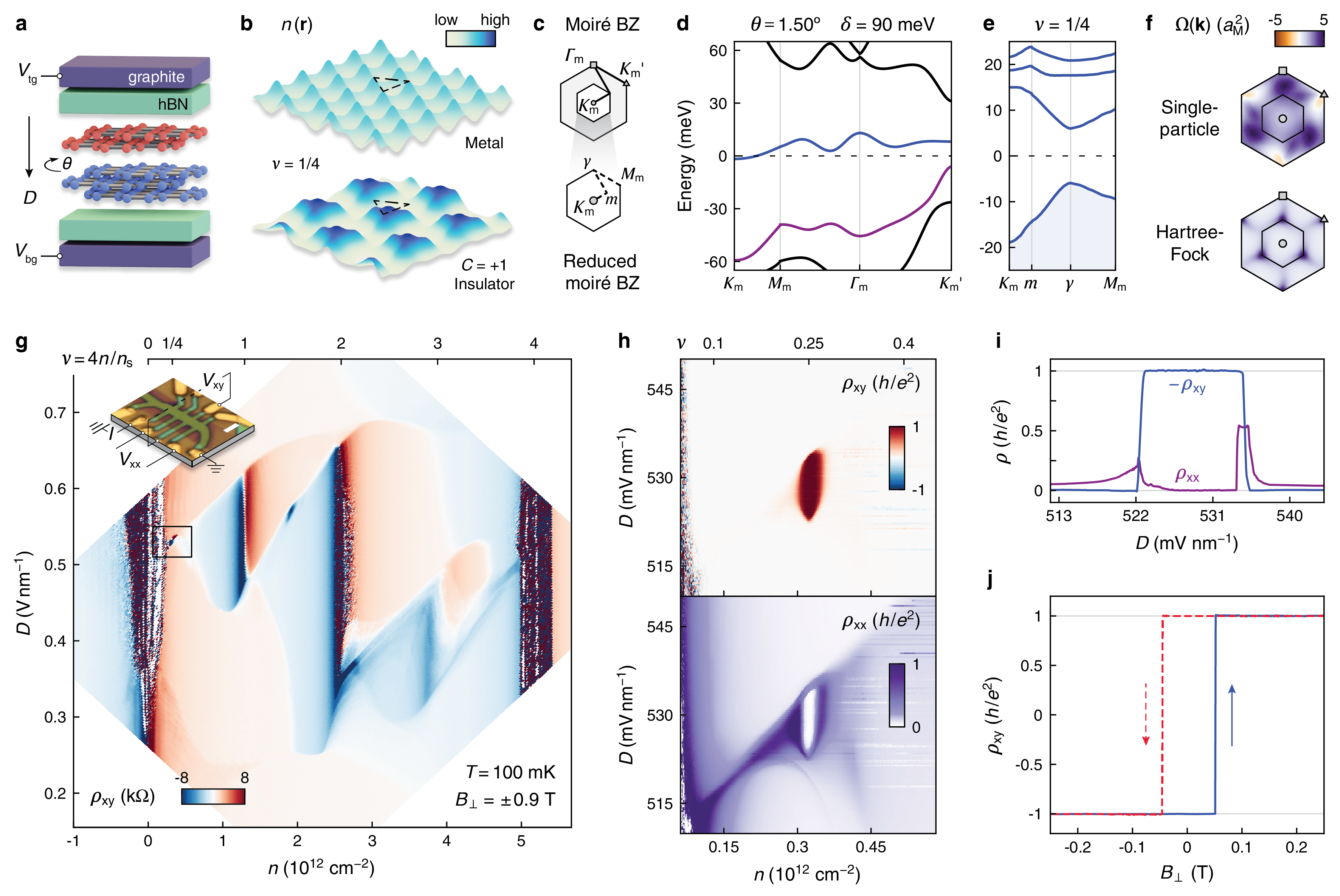
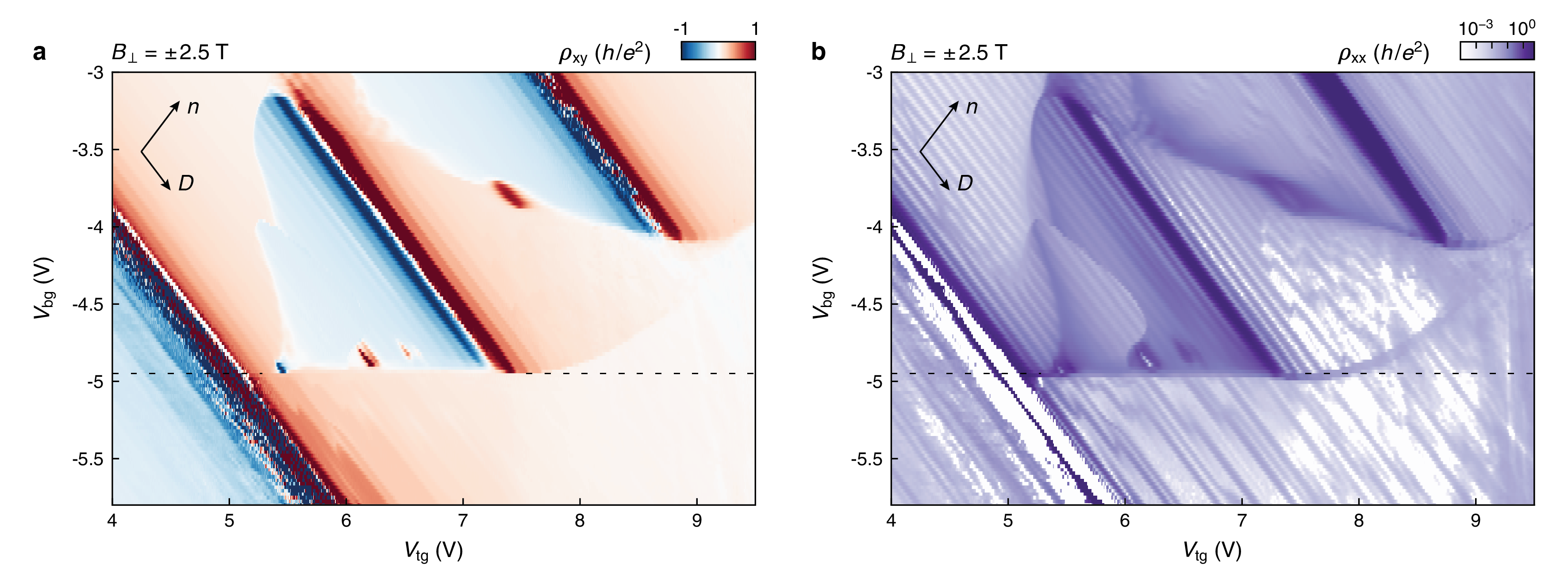
Figure 1a shows the sample structure, consisting of Bernal-stacked bilayer and trilayer flakes twisted by with respect to each other (see Extended Data Fig. 1), as well as top and bottom graphite gates that can be used to tune the carrier density , and displacement field, . The band structure depends both on the magnitude and sign of , owing to the difference in the number of graphene layers above and below the moiré interface. In this work, we focus on electronic states that emerge for , such that the conduction band is polarized towards the trilayer graphene waters2024topological . Figure 1c shows a representative single-particle band-structure calculation for the system (see Methods), including a potential difference between the top and bottom layers, , to capture the effect of an applied . The flat, isolated moiré conduction band (blue curve) is conducive to the spontaneous symmetry-breaking that is essential for the generalized AHC state to emerge. Indeed, this band has previously been observed to host multiple states that break spin and/or valley (together called isospin) degeneracy waters2024topological .
Signatures of isospin symmetry-breaking can be easily seen in a map of the antisymmetrized Hall resistivity, , shown in Fig. 1g. There are multiple instances in which diverges and changes its sign over a narrow range of with essentially no dependence on , corresponding to the chemical potential traversing an energy gap. For example, these features occur at the charge neutrality point (), and at cm-2 where the lowest conduction band is fully filled with four electrons per moiré unit cell (, see Methods). Both are consistent with the expectation of single-particle gaps from the calculated band structure (Fig. 1d). Similar features at quarter– and half–fillings (, and also weakly at ) reflect correlation-induced energy gaps. Our data are broadly similar to previous reports across the family of small–angle twisted multilayer graphene structures Shen2020 ; Liu2020 ; Cao2019b ; Burg2019 ; He2021tdbg ; chen2020tMBG ; polshyn2020electrical ; Xu2021tmbg ; waters2024topological .
.2 Evidence for the generalized anomalous Hall crystal
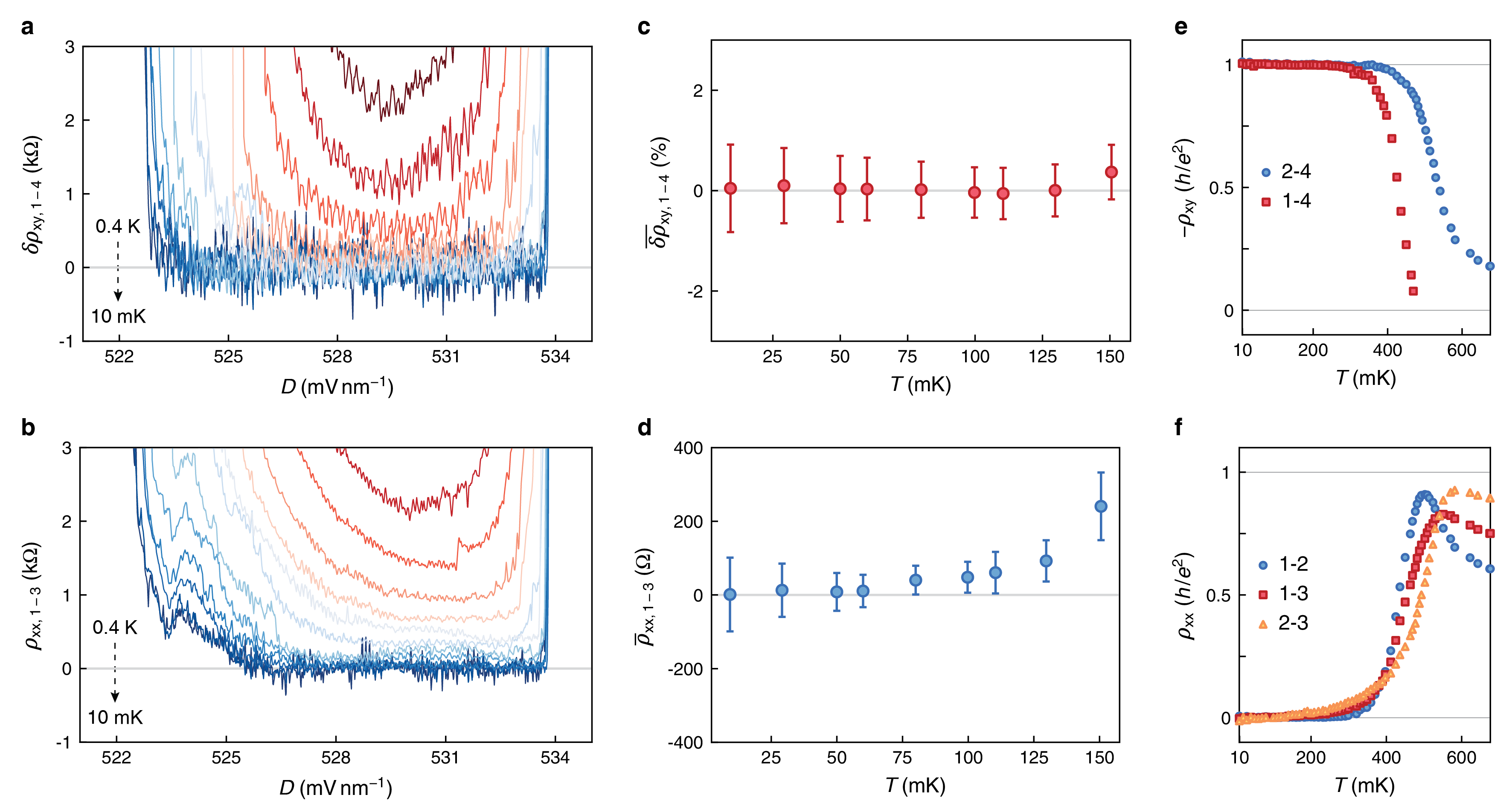
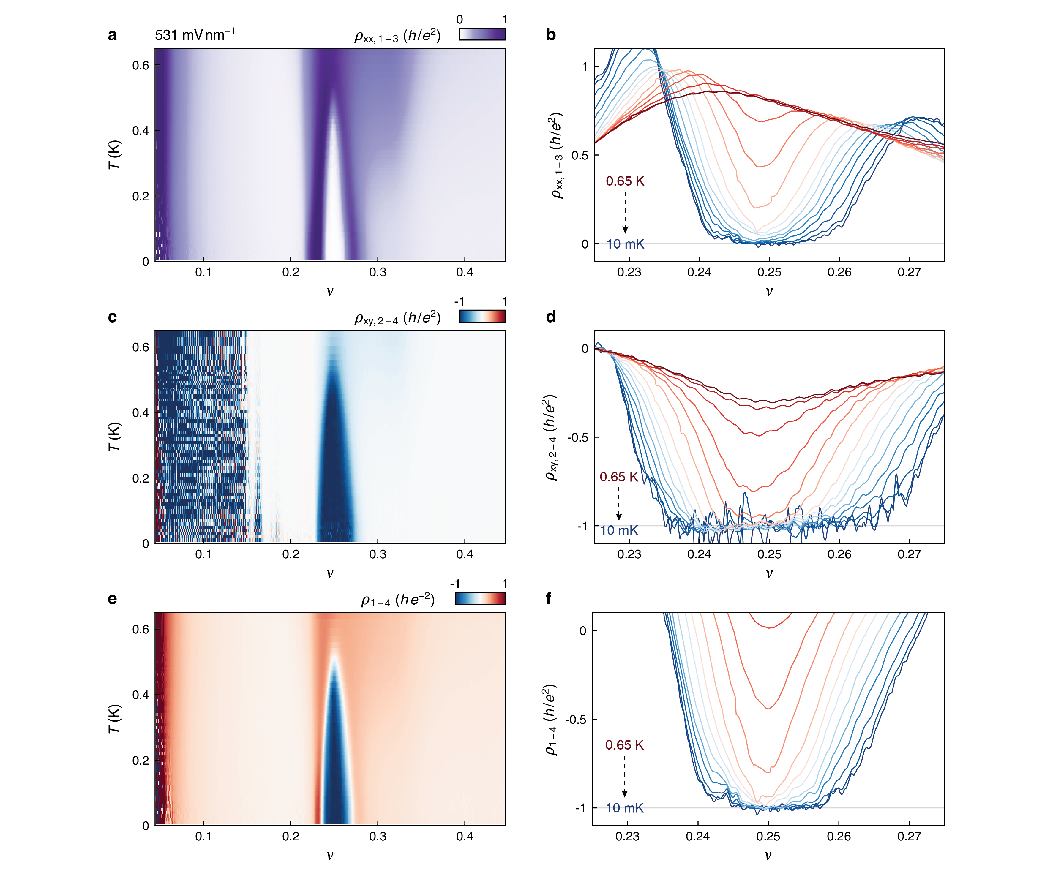
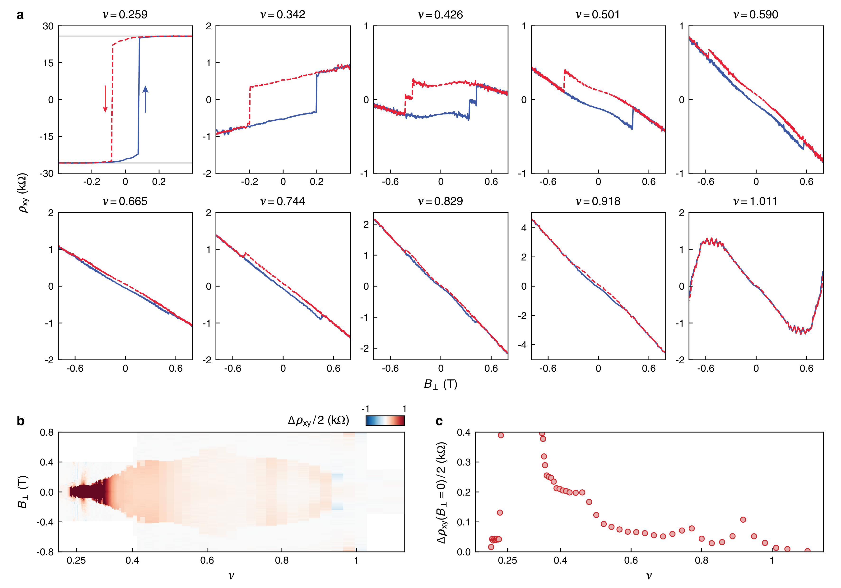
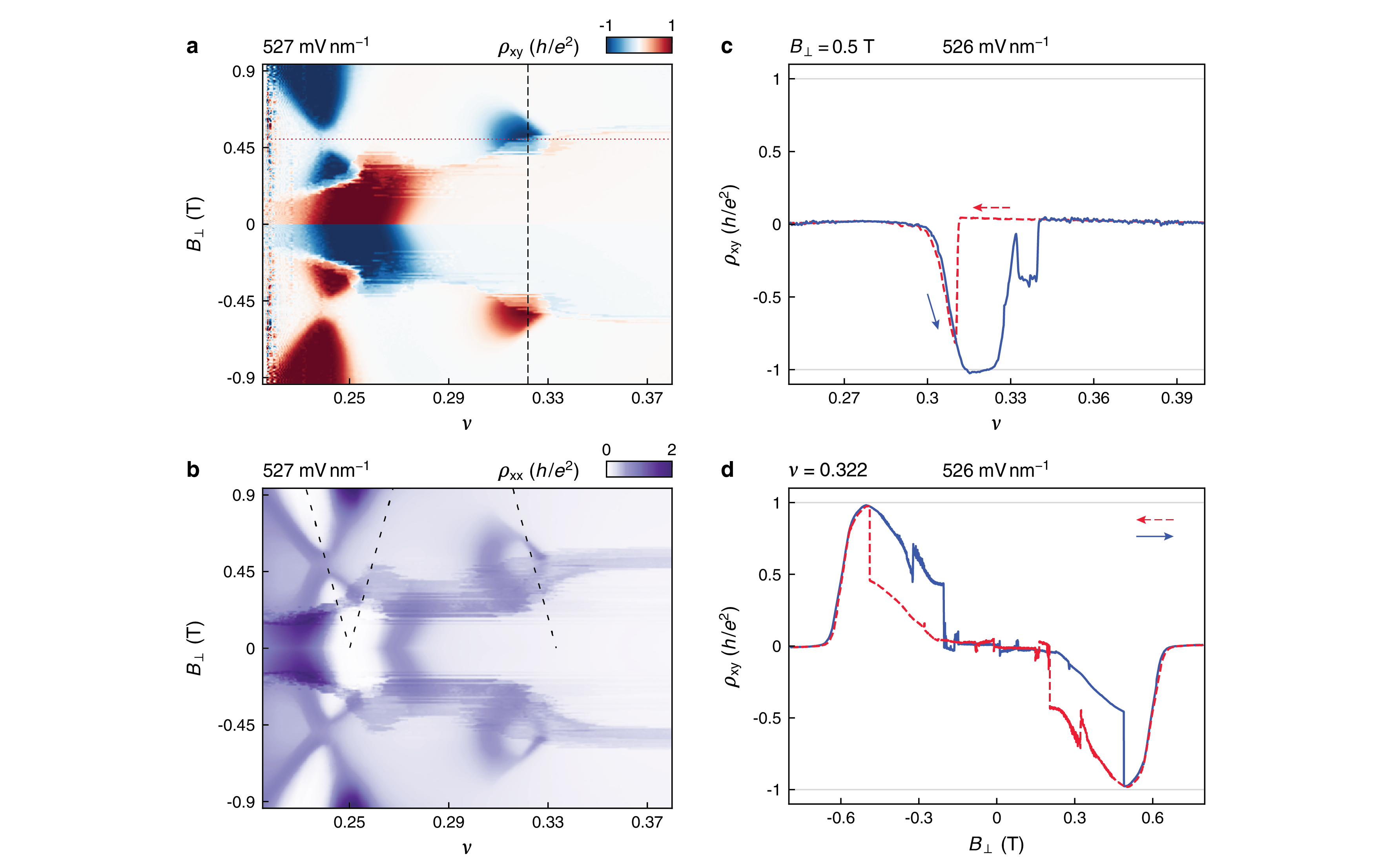
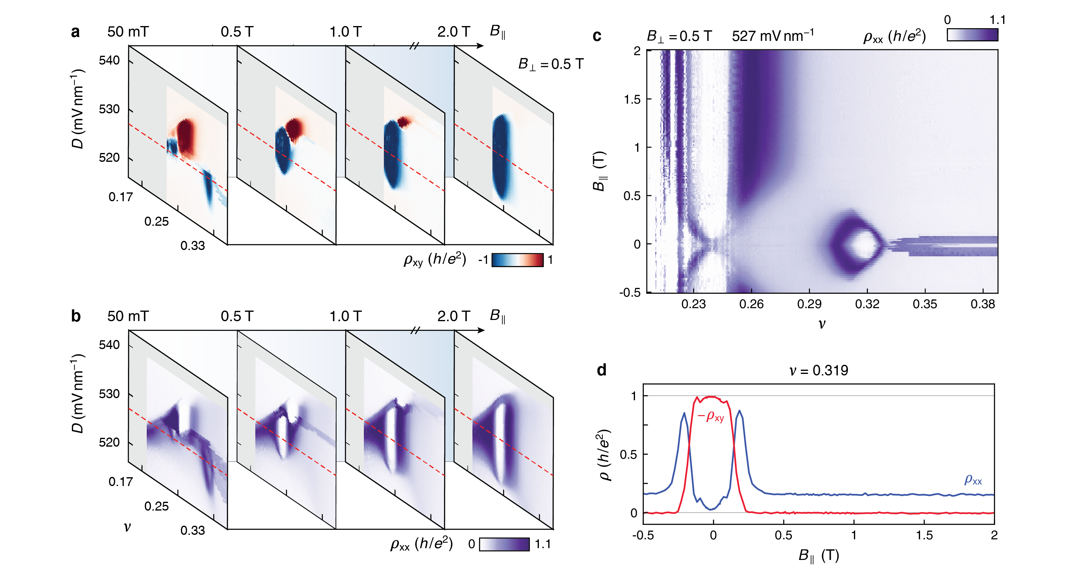
We focus first on one symmetry-broken state that appears very close to charge neutrality and around V nm-1, within the boxed region in Fig. 1g. Figure 1h maps out and over this region near zero field. Remarkably, a stripe of large close to k emerges from a comparably featureless background. The carrier density where the stripe appears, cm-2, corresponds to adding one electron for every four moiré unit cells (). This quantized Hall resistance, concomitant with a vanishing , is a hallmark of an integer QAH state (Fig. 1i). Accordingly, the quantization of persists to zero external magnetic field and up to a temperature of mK (see Extended Data Figs. 2 and 3), and is sharply hysteretic with a coercive field mT (Fig. 1j). The sign of flips abruptly across to form a single square loop. The formation of a gapped topological state with integer quantization of at a doping less than necessitates the simultaneous breaking of time-reversal and translational symmetry, corresponding to a generalized AHC.
The quantized value indicates that the state has a Chern number of , which is confirmed by its evolution in with out-of-plane magnetic field (Fig. 2a). As an applied modifies the degeneracy of filled Chern bands, the charge density required to reach a topological gap changes with . This is described by the Streda formula, , which relates the slope of the trajectory of a gapped state in the plane to its Chern number streda1982quantised ; streda1982theory . The locations of the plateau and minima indeed disperse to larger values of as is increased from zero, in excellent agreement with the expected slope of a state.
Analogous measurements made at show that the state corresponding to a fully filled first moiré band is a gapless metal at zero magnetic field, although it exhibits an anomalous Hall effect upon doping (see Extended Data Figs. 4 and 5). The state transitions to an insulator with upon application of a small , with diverging and an abrupt sign flip in , neither of which disperse in doping as is raised (Extended Data Fig. 5). Thus, the QAH state at appears to emerge directly out of a quarter–metal phase associated with full isospin degeneracy lifting at , as identified by the frequency of quantum oscillations formed in a small magnetic field waters2024topological . The disconnect between for the state at versus at is an identifying characteristic of the anomalous Hall crystal.
.3 Competing topological states
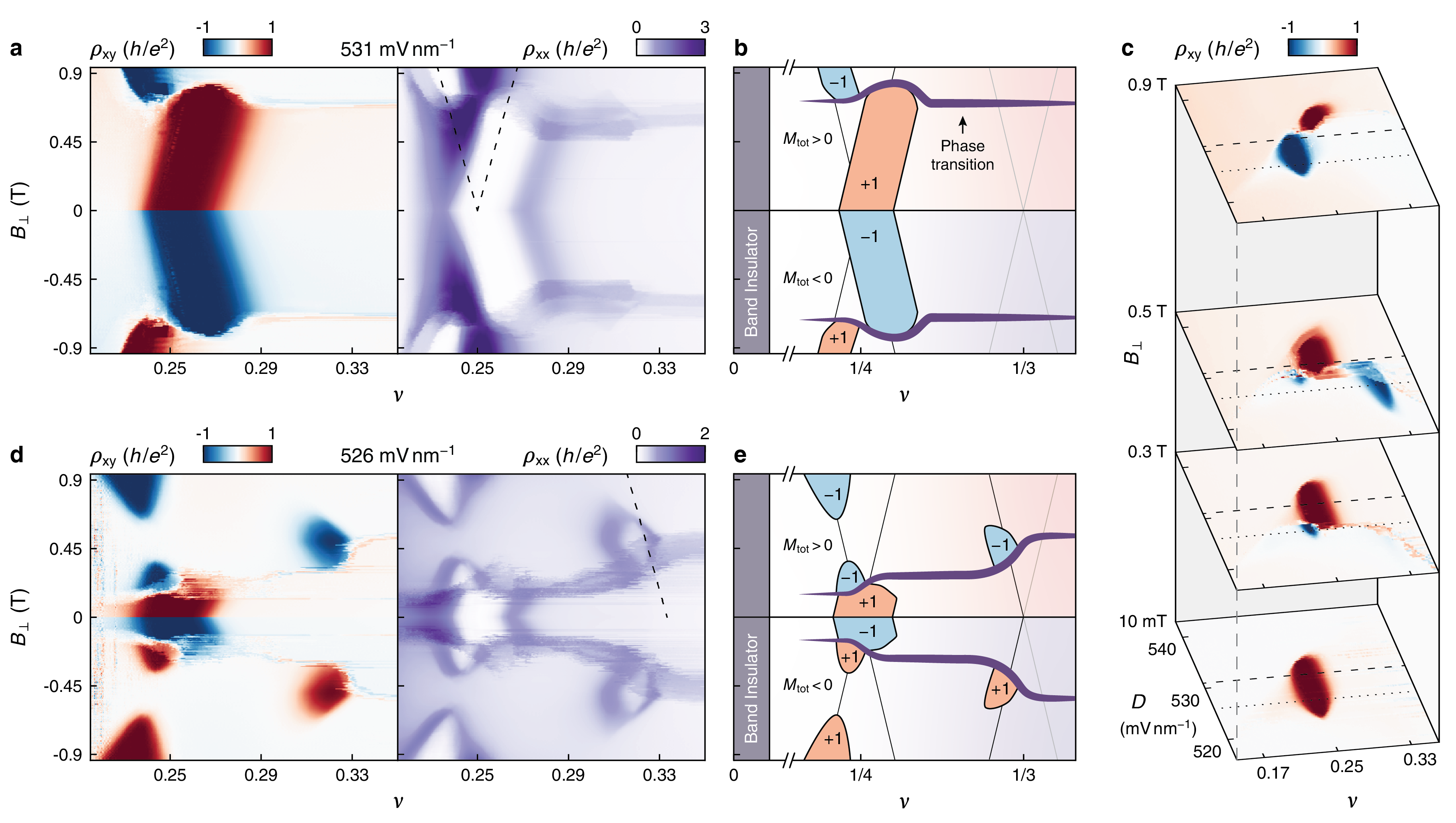
Following the trajectory of the state in Fig. 2a to increasing reveals another remarkable feature of the data: the plateau disappears above T, simultaneous with the emergence of a plateau and minimum. This state arises at a lower charge density () than its zero-field counterpart, consistent with a state also originating from . For clarity, we label these states by their Chern number and band filling upon extrapolation to : and . Apparently, the system undergoes a phase transition above a critical threshold field, , from into a new ground state that also has a quadrupled unit cell but the opposite sign of the Chern number ( ). This transition is first-order in nature, as evidenced by hysteretic jumps in resistance near (see Extended Data Fig. 6). The topological phases represented by the data in Fig. 2a are summarized in Fig. 2b. The sign reversal of across is qualitatively distinct from the flip between states across the coercive field nearer to . Whereas the latter occurs between time-reversed counterparts whose free energies either increase or decrease with , the former cannot be explained in the same way.
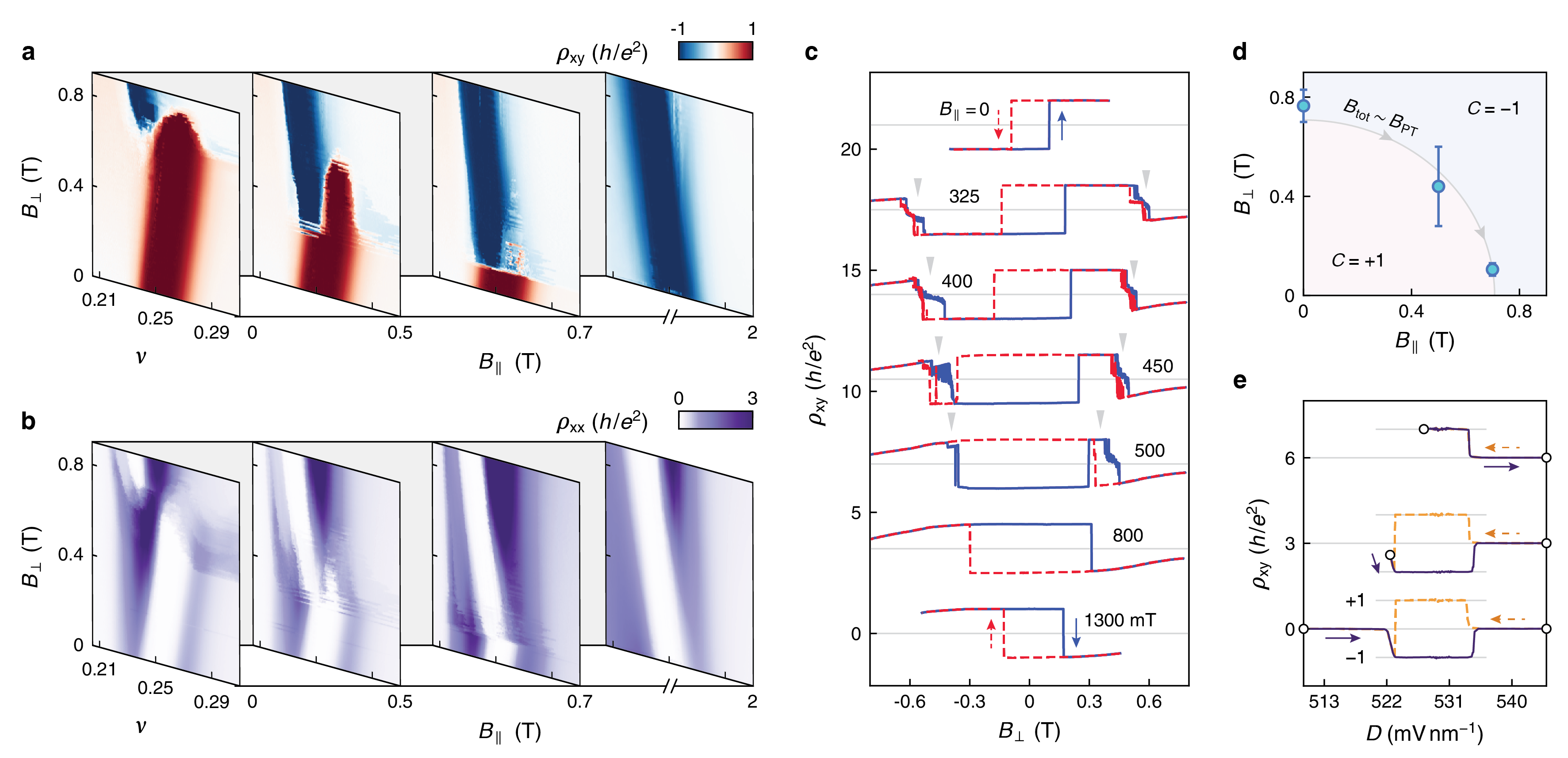
Signatures of the first-order phase transition persist across the entire range of shown in Fig. 2a, indicating that it is not limited to commensurate filling. The transition is also tuned by , as seen in maps of acquired at different fixed values of (Fig. 2c). The primary features of each of these maps are the contiguous regions of red and blue coloring, which correspond to gapped states with and , respectively. The Landau fans shown in Fig. 2a correspond to the value of denoted by the black dashed line. The first-order phase transition seen in Fig. 2a appears as an arc in the plane in Fig. 2c, mapping out the location of this phase transition in both and . At all values of , the arc sharply separates regions of the maps with opposite signs of in the topological gapped states, and with slightly different values of in the metallic states.
.4 Additional magnetic-field–induced states
The map acquired at T in Fig. 2c reveals an additional pocket of quantized Hall resistance close to , where . Figure 2d shows a Landau fan acquired at mV nm-1, corresponding to the black dotted line in Fig. 2c, which cuts through this additional blue pocket at T. The sequence of phase transitions observed at this value of is more intricate, as summarized schematically in Fig. 2e. The extra blue pocket in the T map from Fig. 2c can now be seen as a plateau with concomitant minimum that falls along the line coming from (i.e., ). The appearance of the state is clearly connected with the same first-order phase transition that results in a flip between the and states. The integer Chern number and fractional filling factor of suggest a spontaneously tripled moiré unit cell, contrasting with the quadrupled unit cells of and . Further raising suppresses , and returns (Fig. 2d). Taken together, the data in Fig. 2 indicate that the system switches sharply between a low-field state where the Chern number is and the unit cell is quadrupled, into a higher-field state where the Chern number is and the unit cell may be either tripled or quadrupled, depending on and other parameters.
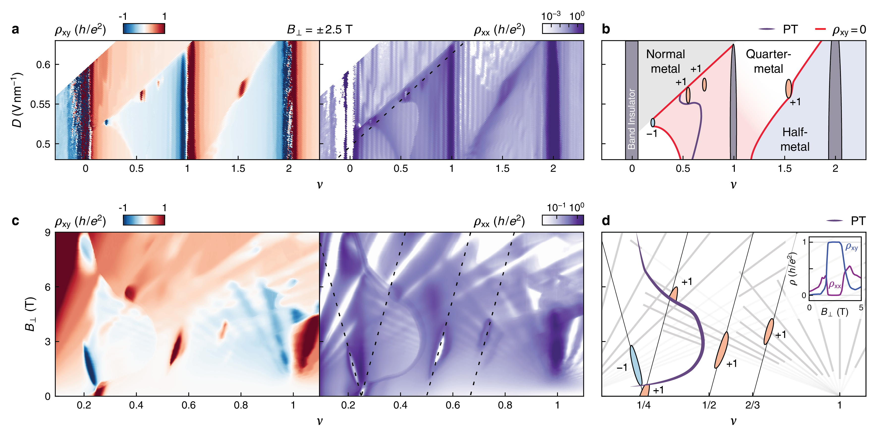
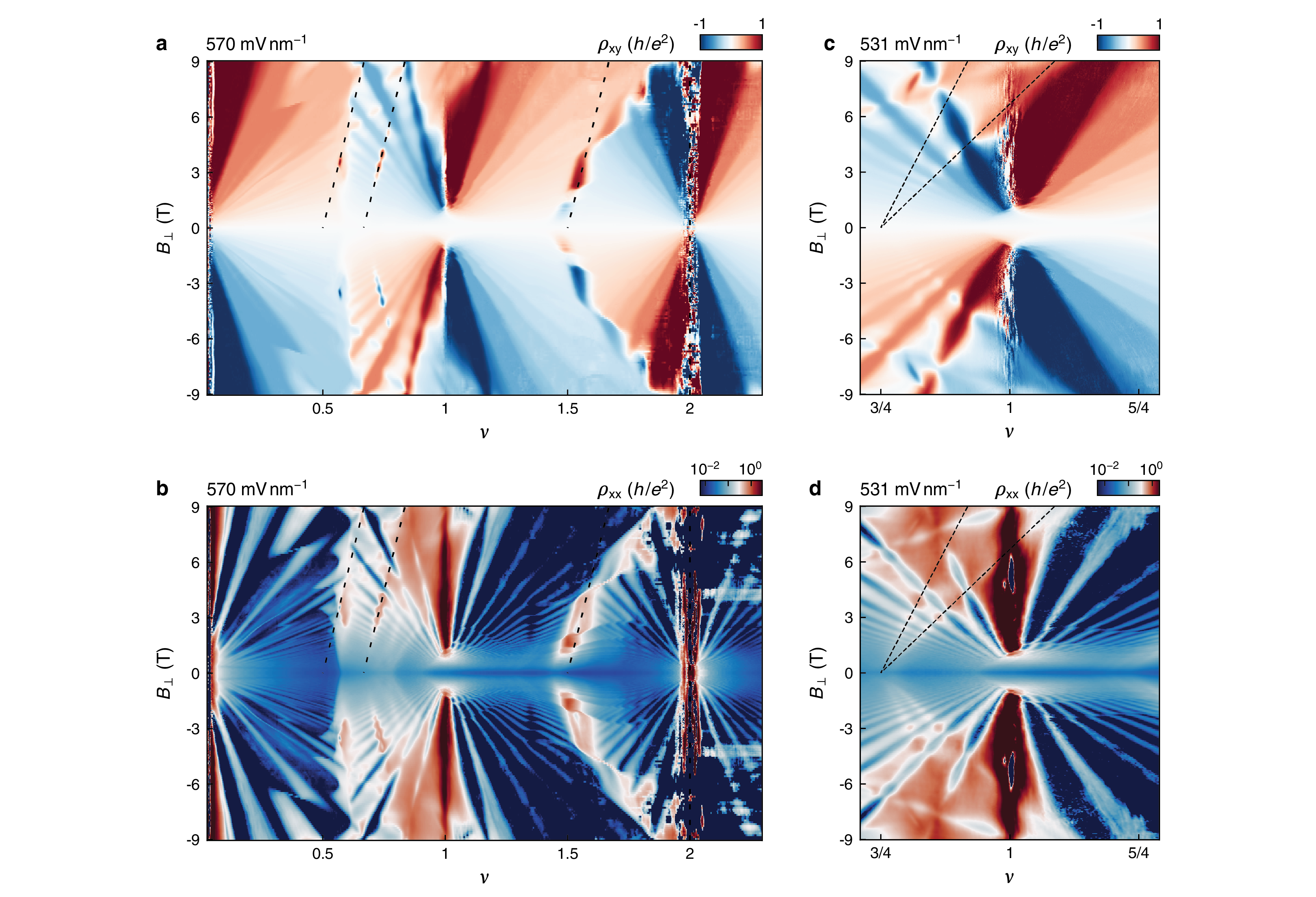
Several other TCDW states arise at even higher perpendicular magnetic fields. Figure 3a shows maps of and at T. A large portion of these maps is covered by extended vertical stripes that correspond to quantum Hall states at fixed band filling. In addition, very small pockets of suppressed and enhanced appear over narrow ranges of , denoted by the states in the schematic diagram (Fig. 3b). With the exception of the state near , all of these features appear along the sharp diagonal boundary that separates the isospin-unpolarized phase at large from the quarter-metal phase at smaller . Notably, this phase boundary is aligned precisely to the axis corresponding to the top gate voltage, , such that the phase transition is controlled entirely by the back gate voltage, (see Extended Data Fig. 7 for the same maps displayed against and ). Although we do not fully understand the origin of this effect, similar behavior is seen across a wide family of symmetry-breaking transitions in twisted Bernal graphene multilayer structures Shen2020 ; Liu2020 ; Cao2019b ; Burg2019 ; He2021tdbg ; chen2020tMBG ; polshyn2020electrical ; Xu2021tmbg ; waters2024topological . We speculate that it may arise from inhomogeneous electrostatic charging of the five layers of graphene rickhaus2019gap ; kolavr2023electrostatic .
In order to better visualize the field-induced TCDW states, we examine a Landau fan acquired along a trajectory parallel to the quarter-metal phase boundary (Fig. 3c, taken along the path denoted by the black dashed line in Fig. 3a), with salient features highlighted in Fig. 3d. The first-order phase transition between the and states that was analyzed earlier appears first at and T, identified in the data by a sharp jump in and an inversion in . The phase transition shifts rapidly towards larger values of as the field is raised and then eventually reverses direction back towards . Notably, the state briefly recurs for T, when the phase transition crosses back across the value of corresponding to the projected trajectory of the state. We speculate later about the possible nature of this first-order phase transition.
At larger values of , additional states arise over small ranges of that project back to and . The state projecting to has a slope corresponding to a Chern number of (i.e., ), consistent with its quantized value of (see the inset of Fig 3d). Similar behavior is seen for a more weakly developed state projecting to , although the Landau fan also shows faint signs of an incipient state at slightly smaller (i.e., and ). Another Landau fan acquired at fixed V/nm, shown in Extended Data Fig. 5a,b, also shows evidence of a weakly developed state projecting to (i.e., ). We speculate that these high-field states are essentially the same as the generalized AHC at but only emerge in a modest external magnetic field (as a matter of terminology, we only refer to states directly connected to as ‘generalized AHC’ states, otherwise we use the more general ‘TCDW’ nomenclature). We also see weak signatures of high-field translational symmetry breaking tracing to , but without any associated gapped TCDW states (see Landau fans in Extended Data Fig. 5c,d). The state projecting to most likely corresponds to a filling of the lowest two folded subbands of a TCDW state with a tripled moiré unit cell area. The states projecting to and could correspond either to filling the lowest of two folded subbands of a TCDW state that doubles the moiré unit cell, or to the filling of multiple subbands of a quadrupled unit cell state. Spatially resolved measurements will be required to distinguish these possibilities.
.5 Chern number control of the generalized AHC
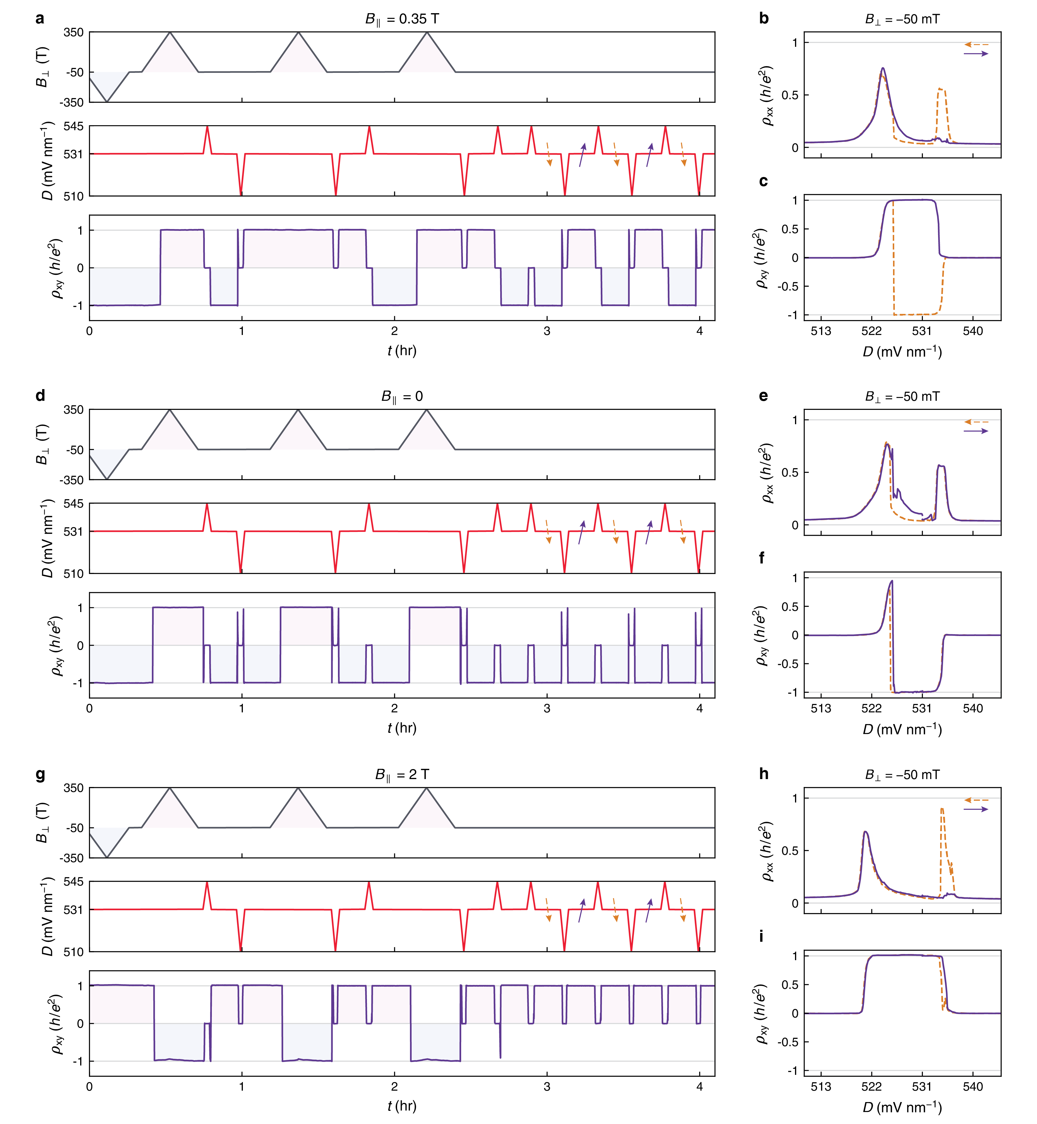
We now return to the nature of the sign reversal of the Chern number of the generalized AHC at . In addition to the first-order flip with , first seen in Fig. 2, we find that an in-plane magnetic field, , can drive a similar transition. Repeating the scans from Fig. 2a with an additional applied, the transition from the to state shifts to lower for larger (Fig. 4a,b), until becomes the ground state at for sufficiently large (right-most panel of Fig. 4a). This leads to a reversal in the orientation of the primary hysteresis loop centered around , as seen in the high- traces of Fig. 4c. For intermediate values of , secondary hysteresis loops are visible around , corresponding to the flip of the Chern number in the transition between and . The primary and secondary hysteresis loops merge as is raised above a crossover value. A quantitative analysis of the to crossover indicates that this transition occurs when the total magnetic field, , exceeds T (Fig. 4d). Additionally, we find that suppresses the state in the narrow ranges of where it appears (Extended Data Fig. 8).
At finite magnetic field, the reversal of the Chern state can also be driven electrically, as first indicated in Fig. 2c. The purple and yellow curves in Fig. 4e show a measurement of as is swept back and forth across the region of the generalized AHC state, sitting at T and T. The hysteresis loop is now actuated by gate voltages, with quantization to depending on the sweeping direction of . Extended Data Fig. 9 shows that this electrical switching is highly robust and repeatable, arising from the apparent lower energy of compared to at smaller values of .
.6 Discussion
Taken together, our results reveal that topological states driven by simultaneous time-reversal and translational symmetry breaking are ubiquitous in twisted bilayer–trilayer graphene. In this context, the generalized AHC is simply the most robust of these states, persisting all the way down to zero magnetic field. Despite their clear experimental signatures, many fundamental questions remain about the underlying nature of these interaction-induced topological states. One is why this particular moiré lattice acts a favorable platform for hosting zero-field electron-crystal states, where the wide array of other moiré structures, under intense investigation by groups around the world, apparently do not. A closely related system is twisted monolayer–bilayer graphene, which has been reported to exhibit incipient integer QAH effects at and . These effects indicate an interaction-induced doubling of the moiré unit cell polshyn2022topological , and perhaps the formation of a generalized AHC. However, the Chern number of the density-wave states () in that system is half that of the states at integer band filling ( at and ), and thus does not clearly demonstrate the interaction-induced modification of Berry curvature that is one hallmark of the AHC.
The nature of the first-order phase transition separating the and states also remains mysterious. One possibility is that this phase transition represents a recondensation of carriers from one valley of the graphene Brillouin zone into the other. Such a scenario has been previously suggested to explain the charge-doping–induced reversal of the sign of observed in orbital magnetic states at integer in magic-angle twisted bilayer graphene and twisted monolayer-bilayer graphene zhu2020voltage ; polshyn2020electrical ; grover2022chern . This effect is understood to result from a flip in the sign of the total magnetization of the state upon doping across the topological gap, reversing the valley corresponding to the ground state. However, the simplest version of this scenario is not consistent with our data. First, we do not find a first-order reversal in upon doping across the state. More generally, a cursory overview of the data in Fig. 2 indicates that the and phases across the finite-field transition are not a time-reversed pair. In contrast with the near-perfect (anti-)symmetry of the transition across , the states above and below the T transition are clearly different, with much narrower than across the boundary, and no at the equivalent location to despite the fact that the transition passes diagonally through .
An alternative possibility is that the two states represent qualitatively different electronic orders, whether within the same valley or in opposite ones. There are many degrees of freedom that could vary between these two orders, including both isospin textures and the real-space geometry of the electronic crystal. Given the sensitivity of the first-order phase transition to , which typically does not couple strongly to orbital degrees of freedom in 2D materials, it is possible that spin physics might play a role in distinguishing the two states. Extended Data Fig. 10 shows schematic energy diagrams of a possible two-state model consistent with our observations, agnostic to the specific ordering of each state but with the constraint that the two states have opposite Chern numbers for a given sign of their total magnetization in order to explain the flip between and across .
Finally, we discuss possible future directions enabled by our work. First, scanning probe measurements to directly visualize the geometry of the generalized AHC will be critical for unraveling its precise nature. Second, recent theories have predicted that fractional quantum anomalous Hall (FQAH) states can emerge upon partially filling a generalized AHC band zhou2023fractional ; dong2023anomalous , which host emergent quasiparticles with fractional electric charge and anyonic quantum exchange statistics. Indeed, the generalized AHC has been proposed as an explanation for the integer QAH insulator seen at one electron per moiré unit cell () in rhombohedral pentalayer graphene aligned with hBN zhou2023fractional ; dong2023anomalous ; tan2024parent ; soejima2024anomalous ; dong2024stability , out of which FQAH states emerge at lu2024fractional . However, in pentalayer graphene, the state at does not need to break any translation symmetry beyond that of the hBN–graphene moiré lattice, making it nearly impossible to distinguish from a standard Chern insulator. The generalized AHC in twisted bilayer–trilayer graphene, which corresponds to a spontaneous enlargement of the moiré unit cell, provides a more direct opportunity to investigate the possible relationship between topological electron crystals and the FQAH effect. In particular, further studies of this system can help to clarify whether FQAH daughter states can emerge upon doping the generalized AHC, or if the two topological many-body orders directly compete. Finally, future experiments based on more complex device geometries — for example, efforts aiming to proximitize the integer (or potential fractional) QAH states with a superconductor to create non-Abelian Majorana (or parafermion) modes — will benefit enormously from the experimental simplicity of the twisted bilayer–trilayer structure, which only contains the favored Bernal stacking configuration rather than the metastable rhombohedral order.
I Methods
Device fabrication. Mechanically exfoliated graphene flakes with connected bilayer and trilayer regions were first identified using optical microscopy. The bilayer and trilayer regions were then separated using polymer-free anodic oxidation nanolithography Li2018 . The vdW heterostructure was sequentially assembled using a polycarbonate (PC)/polydimethylsiloxane (PDMS) stamp wang2013one in the following order: graphite, hBN, bilayer graphene, trilayer graphene, hBN, graphite. The graphene flakes were rotationally misaligned by by rotating the stage after picking up the bilayer graphene. In principle, this should create a twisted AB-ABA stacking geometry. However, we note that AB-BA stacking faults are known to exist in bilayer graphene flakes Ju2015 and cannot be detected optically. Therefore, it is possible that the device is in a twisted BA-ABA stacking geometry, rather than the assumed AB-ABA configuration. Future work will be needed to resolve whether such a difference in stacking configuration is experimentally meaningful.
After assembly, the completed vdW stack is dropped onto a Si/SiO2 wafer. We used standard electron beam lithography and CHF3/O2 plasma etching to define vdW stacks into a Hall bar geometry and standard metal deposition techniques (Cr/Au) wang2013one to make electrical contact.
Transport measurements. The transport measurements were carried out across two thermal cycles, first in a Bluefors LD dilution refrigerator equipped with a 3-axis superconducting vector magnet and then in a Bluefors XLD dilution refrigerator with a one-axis superconducting magnet. In both systems, the nominal base mixing chamber temperature was mK, as measured by a factory-supplied RuOx sensor. Unless otherwise specified, measurements were carried out at mK. Four-terminal lock-in measurements were performed by sourcing a small alternating current of nA at a frequency Hz, chosen to accurately capture sensitive transport features while minimizing electronic noise. In addition, a global bottom gate voltage of between V and V was applied to the Si substrate to improve the contact resistance.
The charge carrier density, , and the out-of-plane electric displacement field, , were defined according to and , where and are the top and bottom gate capacitance per unit area, is the elementary charge and is the vacuum permittivity. and were estimated using the slope of the gate-voltage–dependent Hall density, , where is the antisymmetrized Hall coefficient. The carrier density, , required to fully fill a four-fold degenerate moiré band was estimated using the same method. Using , the filling factor was defined according to . A twist angle of was estimated from the doping density corresponding to adding four electrons per moiré unit cell = 8, where = 0.246 nm is the lattice constant of graphene.
To reduce geometric mixing between measured longitudinal and transverse voltage when , we plot the field-symmetrized values of resistance. was symmetrized according to , and was antisymmetrized according to .
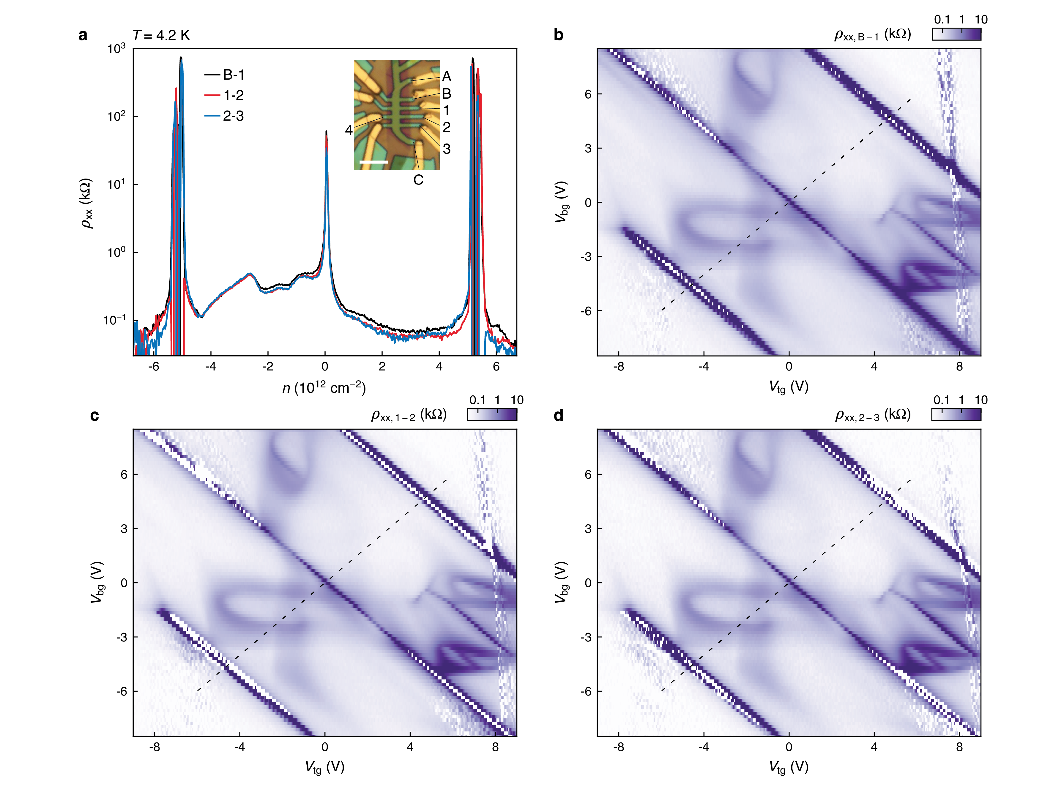
The sample had multiple contacts that could be used as current or voltage probes; these are labelled in the schematic in Extended Data Fig. 1, with differences highlighted in Extended Data Fig. 3. Extended Data Fig. 1 characterizes the sample homogeneity with maps of obtained from several adjacent voltage probes. The maps are nearly identical over the accessible range of gate voltages, providing evidence for a highly homogeneous moiré lattice and minimal twist angle disorder. Except where noted below, measurements used contacts 1 and 3 and measurements used contacts 2 and 4. However, in the following figure panels and measurements were based on the diagonal contact pair 1 and 4 after field symmetrization/antisymmetrization: Fig. 1h; Fig. 2a,c,d; Fig. 3a (left, ); Fig. 4a; Extended Data Fig. 5. Extended Data Fig. 8c used contact pair 2-3 for the measurement. The source and drain contacts are (B,C) throughout.
Band structure calculation. We use the Bistritzer-MacDonald continuum model to calculate the band structure. The Hamiltonian for each valley and spin is:
| (1) |
where and are the Hamiltonian of the bilayer and the trilayer respectively. represents the moiré tunneling between the bilayer and the trilayer. The bilayer Hamiltonian is:
| (2) |
and the trilayer Hamiltonian is:
| (3) |
where , with being the twist angle. The sign corresponds to the bilayer/trilayer respectively. is the potential difference between the top and bottom graphene layers. The hopping parameters are . The moiré tunneling is:
| (4) |
where represents the tunneling between the bottom layer of the bilayer and the top layer of the trilayer, with momentum differences given by . The vectors . We use and in our calculation.
Hartree–Fock calculations. We performed the Hartree–Fock calculation in the reduced Brillouin zone at . The Coulomb interaction term is given by:
| (5) |
where is the density operator at layer , and is the area of system. The interaction potential is defined as:
| (6) |
where is the distance between adjacent layers, is the dielectric constant and is the screening length. We include 4 conduction bands in the reduced BZ at single-particle level and perform the self-consistent calculation. We test random initial ansatzes and select the one with the lowest energy.
Spatial charge distribution calculation. The spatial distribution in Fig. 1(b) is defined as , where is electron annihilation operator in real-space. It can be calculated as:
| (7) |
where is defined in the BZ, is the periodic part of the Bloch wavefunction. is any integer linear combination of reciprocal lattice vectors. For the metallic state, we use the single-particle Bloch wavefunction and sum over below the Fermi energy at . The reciprocal lattice vectors are moiré reciprocal lattice vectors. For the generalized AHC state, we use the Hartree–Fock Bloch wavefunction and sum over in the reduced moiré BZ. The first conduction band is fully filled at . The reciprocal lattice vectors are half the moiré reciprocal lattice vectors.
Berry curvature and Chern number calculation. We use the method from Ref. fukui2005chern, to calculate Berry curvature. The BZ is discretized into an grid. For each in the BZ, we calculate the link:
| (8) |
where and . The Berry curvature is then given by:
| (9) |
where is . We ensure that . For the metallic state, the BZ is the moiré BZ. For the generalized AHC state at , the BZ is the reduced moiré BZ. The Chern number is calculated as:
| (10) |
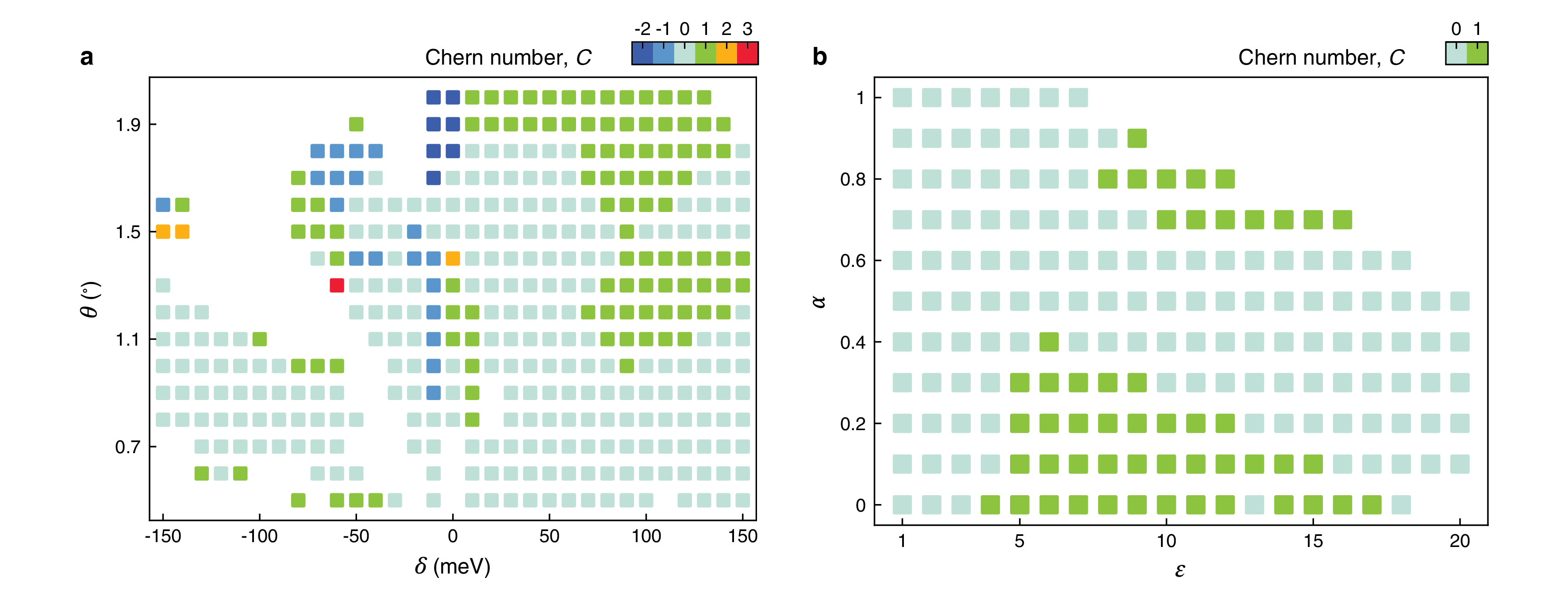
Extended Data Fig. 11 shows the calculated Chern number of the generalized AHC state at as various parameters (, , , and ) are tuned. Our Hartree–Fock calculations predict a state for realistic parameters, consistent with our experiment. However, we caution that we do not know the precise values of any of these parameters experimentally except for , and the calculations also find other Chern number ground states within relatively narrow parameter ranges. Furthermore, Hartree–Fock predicts a generalized AHC state over a substantially wider range of than is observed experimentally; this is consistent with the tendency of Hartree–Fock calculations to underestimate the formation energy of symmetry-broken states. Despite these uncertainties, the states found experimentally and theoretically motivate a plausible connection between the two. The sensitivity of the Chern number in Hartree–Fock calculations to the dielectric screening, , highlights the importance of interactions in determining the topological properties of the electronic crystal.
The valley Chern number of the single-particle moiré conduction band is calculated to be . Based on this, a spin-valley–polarized state at is expected to have since it corresponds to a single filled valley. Because the state at in our device is metallic, it is not possible to extract its Chern number. However, the vanishing AHE at (Extended Data Fig. 4) is inconsistent with a gapless but valley-imbalanced state. Our observation of a correlated insulator at finite field (Extended Data Fig. 5) is also inconsistent with the prediction from the single-particle band structure calculation, although the Chern number of a correlated state at finite need not be the same as its value at . Future work will be necessary to identify the origin of this apparent inconsistency. In any case, the Chern number of for the state is not equal to one-quarter of either of the possible Chern numbers of the parent state at (i.e., or ). Thus, the ambiguity in identifying the latter does not affect our primary conclusion that a combination of band folding and interactions determine the Chern number of the generalized AHC state.
II Acknowledgements
The authors thank Liang Fu, Leon Balents, Marcel Franz, Michael Zaletel, and Andrea Young for helpful discussions. Experiments at UBC were undertaken with support from the Natural Sciences and Engineering Research Council of Canada; the Canada Foundation for Innovation; the Canadian Institute for Advanced Research; the Max Planck-UBC-UTokyo Centre for Quantum Materials and the Canada First Research Excellence Fund, Quantum Materials and Future Technologies Program; and the European Research Council (ERC) under the European Union’s Horizon 2020 research and innovation program, Grant Agreement No. 951541. Work at UW was supported by National Science Foundation (NSF) CAREER award no. DMR-2041972 and NSF MRSEC 1719797. The development of twisted graphene samples was partially supported by the Department of Energy, Basic Energy Science Programs under award DE-SC0023062. D.W. was supported by an appointment to the Intelligence Community Postdoctoral Research Fellowship Program at University of Washington administered by Oak Ridge Institute for Science and Education through an interagency agreement between the US Department of Energy and the Office of the Director of National Intelligence. K.W. and T.T. acknowledge support from the Elemental Strategy Initiative conducted by the MEXT, Japan (grant no. JPMXP0112101001) and JSPS KAKENHI (grant nos. 19H05790, 20H00354 and 21H05233). Y.-H.Z. was supported by the National Science Foundation under Grant No. DMR-2237031. This work made use of shared fabrication facilities at UW provided by NSF MRSEC 1719797.
III Author Contributions
R.S. performed the measurements in the Folk lab at UBC, and analyzed the data; D.W. made the sample and performed initial transport measurements in the Yankowitz lab at UW; M.Y. and J.F. supervised the measurements; R.S., M.Y. and J.F. wrote the manuscript with B.Z. and Y.Z. providing theory support; K.W. and T.T. provided the hBN crystals.
Competing interests
The authors declare no competing interests.
Additional Information
Correspondence and requests for materials should be addressed to Matthew Yankowitz or Joshua Folk.
Data Availability
Source data are available for this paper. All other data that support the findings of this study are available from the corresponding author upon request.
References
- (1) Wigner, E. On the interaction of electrons in metals. Phys. Rev. 46, 1002 (1934).
- (2) Grimes, C. C. & Adams, G. Evidence for a liquid-to-crystal phase transition in a classical, two-dimensional sheet of electrons. Phys. Rev. Lett. 42, 795 (1979).
- (3) Andrei, E. Y. et al. Observation of a magnetically induced Wigner solid. Phys. Rev. Lett. 60, 2765–2768 (1988).
- (4) Zhou, B., Yang, H. & Zhang, Y.-H. Fractional quantum anomalous Hall effects in rhombohedral multilayer graphene in the moiréless limit and in Coulomb imprinted superlattice. arXiv:2311.04217 (2023).
- (5) Dong, J. et al. Anomalous Hall crystals in rhombohedral multilayer graphene I: Interaction-driven Chern bands and fractional quantum Hall states at zero magnetic field. arXiv:2311.05568 (2023).
- (6) Kwan, Y. H. et al. Moiré fractional Chern insulators III: Hartree-Fock phase diagram, magic angle regime for Chern insulator states, the role of the moiré potential and Goldstone gaps in rhombohedral graphene superlattices. arXiv:2312.11617 (2023).
- (7) Sheng, D., Reddy, A., Abouelkomsan, A., Bergholtz, E. & Fu, L. Quantum anomalous Hall crystal at fractional filling of moiré superlattices. arXiv:2402.17832 (2024).
- (8) Tan, T. & Devakul, T. Parent Berry curvature and the ideal anomalous Hall crystal. arXiv:2403.04196 (2024).
- (9) Soejima, T. et al. Anomalous Hall crystals in rhombohedral multilayer graphene II: General mechanism and a minimal model. arXiv:2403.05522 (2024).
- (10) Dong, Z., Patri, A. S. & Senthil, T. Stability of anomalous Hall crystals in multilayer rhombohedral graphene. arXiv:2403.07873 (2024).
- (11) Haldane, F. D. M. Model for a quantum Hall effect without Landau levels: Condensed-matter realization of the ”parity anomaly”. Phys. Rev. Lett. 61, 2015 (1988).
- (12) Chang, C.-Z., Liu, C.-X. & MacDonald, A. H. Colloquium: Quantum anomalous Hall effect. Rev. Mod. Phys. 95, 011002 (2023).
- (13) Thouless, D. J., Kohmoto, M., Nightingale, M. P. & den Nijs, M. Quantized Hall conductance in a two-dimensional periodic potential. Phys. Rev. Lett. 49, 405 (1982).
- (14) Xiao, D., Chang, M.-C. & Niu, Q. Berry phase effects on electronic properties. Rev. Mod. Phys. 82, 1959–2007 (2010).
- (15) Sharpe, A. L. et al. Emergent ferromagnetism near three-quarters filling in twisted bilayer graphene. Science 365, 605–608 (2019).
- (16) Serlin, M. et al. Intrinsic quantized anomalous Hall effect in a moiré heterostructure. Science 367, 900–903 (2020).
- (17) Stepanov, P. et al. Competing zero-field Chern insulators in superconducting twisted bilayer graphene. Phys. Rev. Lett. 127, 197701 (2021).
- (18) Polshyn, H. et al. Topological charge density waves at half-integer filling of a moiré superlattice. Nat. Phys. 18, 42–47 (2022).
- (19) Chen, G. et al. Tunable correlated Chern insulator and ferromagnetism in a moiré superlattice. Nature 579, 56–61 (2020).
- (20) Lu, Z. et al. Fractional quantum anomalous Hall effect in multilayer graphene. Nature 626, 759–764 (2024).
- (21) Li, T. et al. Quantum anomalous Hall effect from intertwined moiré bands. Nature 600, 641–646 (2021).
- (22) Cai, J. et al. Signatures of fractional quantum anomalous Hall states in twisted MoTe2. Nature 622, 63–68 (2023).
- (23) Zeng, Y. et al. Thermodynamic evidence of fractional Chern insulator in moiré MoTe2. Nature 622, 69–73 (2023).
- (24) Park, H. et al. Observation of fractionally quantized anomalous Hall effect. Nature 622, 74–79 (2023).
- (25) Tao, Z. et al. Valley-coherent quantum anomalous Hall state in AB-stacked MoTe2/WSe2 bilayers. Phys. Rev. X 14, 011004 (2024).
- (26) Han, T. et al. Large quantum anomalous Hall effect in spin-orbit proximitized rhombohedral graphene. Science 384, 647–651 (2024).
- (27) Sha, Y. et al. Observation of Chern insulator in crystalline ABCA-tetralayer graphene with spin-orbit coupling. Science 384, 414–419 (2024).
- (28) Tešanović, Z., Axel, F. & Halperin, B. “Hall crystal” versus Wigner crystal. Phys. Rev. B 39, 8525 (1989).
- (29) Wang, L. et al. Evidence for a fractional fractal quantum hall effect in graphene superlattices. Science 350, 1231–1234 (2015).
- (30) Spanton, E. M. et al. Observation of fractional chern insulators in a van der waals heterostructure. Science 360, 62–66 (2018).
- (31) Saito, Y. et al. Hofstadter subband ferromagnetism and symmetry-broken chern insulators in twisted bilayer graphene. Nat. Phys. 17, 478–481 (2021).
- (32) Xie, Y. et al. Fractional chern insulators in magic-angle twisted bilayer graphene. Nature 600, 439–443 (2021).
- (33) He, M. et al. Symmetry-broken chern insulators in twisted double bilayer graphene. Nano Lett. 23, 11066–11072 (2023).
- (34) Xie, Y. et al. Strong interactions and isospin symmetry breaking in a supermoiré lattice. arXiv:2404.01372 (2024).
- (35) Waters, D. et al. Topological flat bands in a family of multilayer graphene moiré lattices. arXiv:2405.05913 (2024).
- (36) Shen, C. et al. Correlated states in twisted double bilayer graphene. Nat. Phys. 16, 520–525 (2020).
- (37) Liu, X. et al. Tunable spin-polarized correlated states in twisted double bilayer graphene. Nature 583, 221–225 (2020).
- (38) Cao, Y. et al. Tunable correlated states and spin-polarized phases in twisted bilayer–bilayer graphene. Nature 583, 215–220 (2020).
- (39) Burg, G. W. et al. Correlated insulating states in twisted double bilayer graphene. Phys. Rev. Lett. 123, 197702 (2019).
- (40) He, M. et al. Symmetry breaking in twisted double bilayer graphene. Nat. Phys. 17, 26–30 (2021).
- (41) Chen, S. et al. Electrically tunable correlated and topological states in twisted monolayer–bilayer graphene. Nat. Phys. 17, 374–380 (2021).
- (42) Polshyn, H. et al. Electrical switching of magnetic order in an orbital Chern insulator. Nature 588, 66–70 (2020).
- (43) Xu, S. et al. Tunable van Hove singularities and correlated states in twisted monolayer–bilayer graphene. Nat. Phys. 17, 619–626 (2021).
- (44) Streda, P. Quantised Hall effect in a two-dimensional periodic potential. J. Phys. C 15, L1299 (1982).
- (45) Streda, P. Theory of quantised Hall conductivity in two dimensions. J. Phys. C 15, L717 (1982).
- (46) Rickhaus, P. et al. Gap opening in twisted double bilayer graphene by crystal fields. Nano Lett. 19, 8821–8828 (2019).
- (47) Kolář, K., Zhang, Y., Nadj-Perge, S., von Oppen, F. & Lewandowski, C. Electrostatic fate of n-layer moiré graphene. Phys. Rev. B 108, 195148 (2023).
- (48) Zhu, J., Su, J.-J. & MacDonald, A. H. Voltage-controlled magnetic reversal in orbital chern insulators. Phys. Rev. Lett. 125, 227702 (2020).
- (49) Grover, S. et al. Chern mosaic and Berry-curvature magnetism in magic-angle graphene. Nat. Phys. 18, 885–892 (2022).
- (50) Li, H. et al. Electrode-free anodic oxidation nanolithography of low-dimensional materials. Nano Lett. 18, 8011–8015 (2018).
- (51) Wang, L. et al. One-dimensional electrical contact to a two-dimensional material. Science 342, 614–617 (2013).
- (52) Ju, L. et al. Topological valley transport at bilayer graphene domain walls. Nature 520, 650–655 (2015).
- (53) Fukui, T., Hatsugai, Y. & Suzuki, H. Chern numbers in discretized Brillouin zone: efficient method of computing (spin) Hall conductances. J. Phys. Soc. Jpn. 74, 1674–1677 (2005).
Extended Data
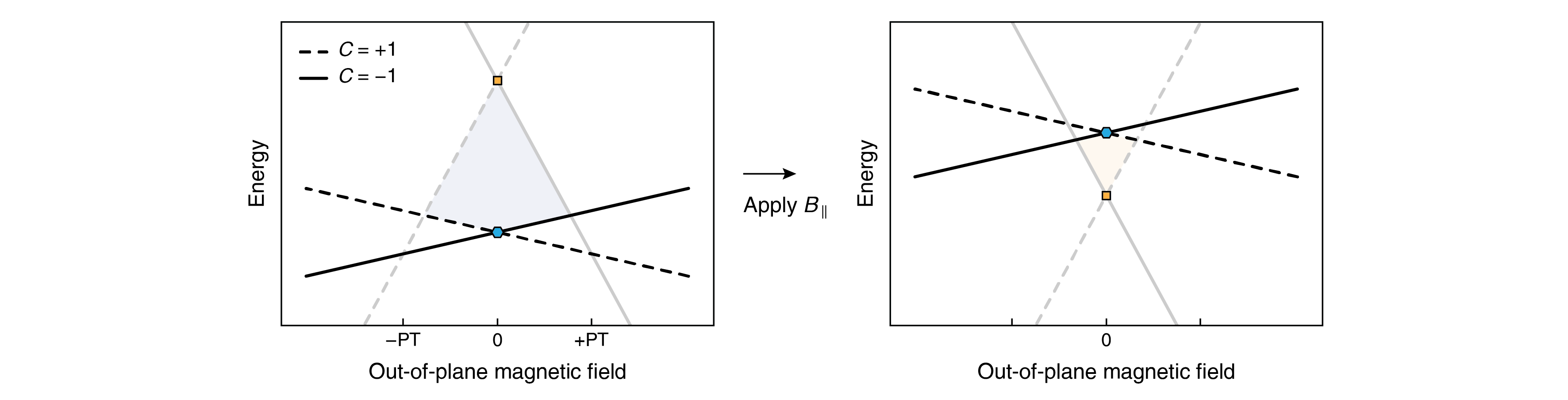
The model is agnostic to the precise details of the two different states, but assumes that the magnetization of the state marked by the yellow square is larger than that of the state marked by the blue dot, and also that the direction of magnetization for a given sign of Chern number is opposite for the two states. The second assumption is plausible because there is, in general, no fixed relationship between the sign of and the sign of the total magnetization for orbital magnetic states. The energies of the and branches of each state evolve oppositely in an applied out-of-plane field, and their magnetization is proportional to the slope of these lines. Above a certain value of , one branch of the state with larger magnetization (yellow square) has a lower energy than either branch of the original ground state (blue circle). The crossing points are denoted as “PT”, indicating the value of at which a first-order phase transition between the two states is anticipated. For each state, the sign of the Chern number of the branch with lower energy in an applied corresponds to which has its total magnetization aligned with the external field.
These are a minimal set of assumptions needed to explain the reversal in the sign of the Chern number across . In this model, the additional reversal with could result from its coupling to the energetic hierarchy of the two states at fixed . For instance, could lower the energy of the state marked by the yellow square to a value lower than that of the state marked by the blue circle, thus making the former the ground state. A similar ground state reversal may also result from changing , explaining the gate-induced hysteresis at fixed and . Although these models are consistent with all of our measurements, we cannot rule out alternative explanations not considered here.