Robust Pareto Design of GaN HEMTs for Millimeter-Wave Applications
Abstract
This paper introduces a robust Pareto design approach for selecting Gallium Nitride (GaN) High Electron Mobility Transistors (HEMTs), particularly for power amplifier (PA) and low-noise amplifier (LNA) designs in 5G applications. We consider five key design variables and two settings (PAs and LNAs) where we have multiple objectives. We assess designs based on three critical objectives, evaluating each by its worst-case performance across a range of Gate-Source Voltages (). We conduct simulations across a range of values to ensure a thorough and robust analysis. For PAs, the optimization goals are to maximize the worst-case modulated average output power () and power-added efficiency () while minimizing the worst-case average junction temperature () under a modulated 64-QAM signal stimulus. In contrast, for LNAs, the focus is on maximizing the worst-case maximum oscillation frequency () and Gain, and minimizing the worst-case minimum noise figure (). We utilize a derivative-free optimization method to effectively identify robust Pareto optimal device designs. This approach enhances our comprehension of the trade-off space, facilitating more informed decision-making. Furthermore, this method is general across different applications. Although it does not guarantee a globally optimal design, we demonstrate its effectiveness in GaN device sizing. The primary advantage of this method is that it enables the attainment of near-optimal or even optimal designs with just a fraction of the simulations required for an exhaustive full-grid search.
1 Introduction
Gallium Nitride (GaN) high-electron-mobility transistors (HEMTs) have gained significant attention at millimeter-wave (mm-wave) frequencies thanks to their superior high-power and low-noise performance compared to other III-V and silicon-based semiconductor technologies. These devices are primarily utilized in power amplifiers (PAs), where GaN’s intrinsic material properties enable high output power () and power-added-efficiency (PAE) across the mm-wave spectrum, which is vital for RF systems in current and emerging wireless links such as 5G and beyond-5G [MPW02, MSKW08, LZY+23, WBN+24]. While their predominant use is in PAs, GaN HEMTs also demonstrate remarkable capabilities in low-noise amplifier (LNA) applications due to material properties such as high mobility from the two-dimensional electron gas (2DEG) and peak saturation velocity (). This is because the high electron mobility, facilitated by the 2DEG, significantly reduces the scattering probability of electrons, leading to lower electron transit times and directly contributing to reduced noise. Furthermore, the high allows electrons to traverse the transistor rapidly, minimizing noise-generating scattering events [Lie76, Pos89, L+09]. Therefore, GaN HEMTs not only exhibit superior breakdown voltage and ruggedness due to the wide bandgap when compared to other III-V high-performance semiconductor technologies (e.g., indium phosphide and gallium arsenide) but also offer competitive noise figure (NF) values. This combination of attributes facilitates lower noise amplification and enhanced reliability, making it particularly advantageous in 5G-and-beyond and defense applications [Mea23].
Even with the adoption of a high-performance semiconductor technology like GaN, the development of PAs and LNAs remains challenging due to the multifaceted design space, which involves numerous trade-offs. As an example, in the context of 5G technology and PA design, spectrally efficient modulation schemes such as orthogonal frequency-division multiplexing (OFDM), higher-order quadrature amplitude modulations (QAMs), and carrier aggregations are employed to maximize the throughput of the communication channels. In order to maintain a high signal fidelity, stringent linearity standards are imposed in the form of adjacent channel power ratio (ACPR) and error vector magnitude (EVM). As such, PAs are forced to operate below their peak output power () level to comply with these requirements, which significantly reduces the modulated average output power () and average amplifier efficiency () compared to their peak continuous wave (CW) performance. This problem is further exacerbated by device-level issues such as soft compression, dc-RF dispersion, and self-heating, which reduce the device’s output power, power-added-efficiency (PAE), and linearity [MMS+23, LZY+23]. In particular, as self-heating effects intensify, the device’s junction temperature () rises, leading to reduced channel mobility and, consequently, a lower drain current (). This sets a boundary on the maximum achievable , PAE, and the overall operational lifetime of the device. From a reliability standpoint, prior research using the same GaN process as in this study has demonstrated that reducing by 40C significantly enhanced the mean time to failure (MTTF) in RF accelerated life tests by an order of magnitude [G+22].
In LNA design, a direct trade-off exists between the minimum achievable NF and maximum Gain [Gon96]. As one of the initial stages in the receiver, the NF of the LNA must be minimized since the noise contribution of each subsequent stage is less significant as the Gain of the first stage minimizes the noise contribution of the proceeding stages, as suggested by Friis’ equation [Fri44]. On top of that, there is also a trade-off between power consumption and LNA performance (e.g., Gain, NF, and linearity), as reducing power consumption generally comes at the expense of lower performance. However, linearity is not typically the main concern in LNAs since the linearity limitations for receivers are more prominent at subsequent stages of the receiver. It is these later stages that primarily determine the receiver’s overall third-order-intercept point () or 1 dB compression point (). An exception to this is in wideband receivers, which might encounter numerous strong interfering signals [Raz11].
Given the previously described challenges, a major concern for circuit designers is choosing the optimal device size for their intended application. Nevertheless, device sizing is a complex multi-objective optimization problem in mm-wave circuit design, typically tackled through iterative trial-and-error methods, rarely leading to a definitive solution. In many instances, the device is optimized without considering the whole design space. Some examples include only maximizing the device for the highest peak unity power gain frequency (), , or PAE performance [DENB05, NP21]. To find the optimal device size, it is important to evaluate the whole design space by taking into consideration the proper metrics for various trade-offs in a PA or LNA. In the present work, we propose a robust Pareto design approach to size GaN HEMTs by evaluating the “worst-case” performance obtained from both LNA and PA metrics and then finding the Pareto optimal values. We utilize a lightweight hyperparameter optimization (HPO) software named Hyperparameter Optimizer: Light-weight and Asynchronous (HOLA) [MBK+22] to aid this approach, which searches and retrieves Pareto optimal points with respect to multiple objectives using derivative-free optimization (DFO). Our DFO method achieves near-optimal or even optimal designs with significantly less simulations than a full-grid search.
Compared to previous multi-objective optimization studies done in various semiconductor technologies, such as in 2D-material-based FETs [WG21], stacked nanosheet transistors [XGC+22], and thermal/mechanical behavior of GaN HEMTs [AEMREH23], the goal of our approach is to create device designs that perform reliably in a carefully controlled environment and across a wide range of conditions in mass production. We primarily focus on robust Pareto optimization to achieve our goal. This systematic design methodology aims to identify system/process settings that remain robust against variability and uncertainty, optimizing for worst-case scenarios across multiple objectives.
This article is organized as follows. Section II describes and formulates the robust optimization approach to sizing GaN HEMTs. In Section III, we use the described Pareto optimization approach by first evaluating modulated large-signal metrics based on a 64-QAM modulation scheme in the context of PA design, followed by the evaluation of small-signal metrics in GaN HEMTs for LNA design. Section V describes our derivative-free approach to retrieving Pareto optimal points using HOLA. Lastly, Section VII concludes this article.
2 Robust Optimization
Robust optimization is a specialized area within the broader field of optimization. It primarily focuses on developing methods and approaches to manage (or reduce) the adverse implications of parameter uncertainty [BJK+24, BTGN09, GMT14, BS07]. Within robust optimization, two approaches are prevalent: statistical and worst-case deterministic. The statistical approach models parameter uncertainty as random variables, aiming to optimize the expected value of the objective under the distribution of these variables. Conversely, the worst-case deterministic approach, which is the core of the present work, assumes a range of potential parameter values and focuses on optimizing the desired outcome under the most unfavorable conditions [BV04]. Analogous to this, in machine learning (ML), this concept is referred to as adversarial, which pertains to a method of evaluation where an “adversary” specifically selects the most challenging or worst-case parameter for operational use and then critically assesses the system by examining its performance. This approach is critical to ensuring the resilience and reliability of ML models, particularly against inputs specifically crafted to test their limits, i.e., adversarial examples [GSS14]. Consequently, the term adversarial optimization is often used interchangeably with worst-case robust optimization.
In engineering design, the principle of worst-case robust optimization transcends beyond optimizing for performance metrics under the most unfavorable conditions. It addresses common oversights in device designs, such as failing to account for known and unknown factors during device usage. For example, some elements of a device’s functionality might be predictable, while others remain uncertain. This uncertainty is particularly relevant in manufacturing, where parameters might vary. Therefore, it is crucial that the design works well, not just for a hand-crafted device but also for devices produced on a large scale. Another oversight is assuming complete knowledge about how the device will be used. During the design phase, it is common to calibrate the device based on known factors, but this can introduce biases. Nonetheless, device parameters can be inherently unpredictable, and this variability worsens during the manufacturing phase.
In the context of device sizing, there are numerous benefits to employing a robust Pareto design methodology. A robust design results in reduced sensitivity, i.e., the designs are less sensitive to manufacturing and operational variations, such as threshold voltage shifts or quiescent point changes during large-signal operation. In addition to these benefits, identifying Pareto designs offers two practical applications that enhance the decision-making process. The first application allows finding a dense set that characterizes the actual trade-off surface, facilitating intelligent discussions about what is achievable. The second application involves identifying a small representative set of designs, enabling designers to choose from various options with a specific metric in mind. This could be a device with high , PAE, linearity, or a combination of the three, thereby providing an informed approach to selecting the most suitable design based on the application requirements.
It is essential to clarify that the concepts of Pareto optimality (multi-objective optimization) and robustness are distinct and address different aspects of device design. Pareto optimality ensures we can trade-off between multiple objectives rather than solely optimizing for one. In contrast, robust optimization ensures that the performance of designs remains satisfactory under variations in manufacturing or operational conditions. Users can opt for either approach, e.g., they might choose to implement only Pareto optimality without incorporating robustness, or vice versa. With this understanding of Pareto optimality and robustness, we proceed to our main objective, which integrates both elements. In the present work, our goal is to identify robust Pareto optimal designs that comprehensively cover the trade-off surface. This approach merges the two concepts discussed above: achieving robustness in design to ensure consistent performance under varying conditions and identifying Pareto optimal points to effectively navigate the trade-offs among multiple objectives.
2.1 Robust Optimization Problem Formulation
In the present work, we encounter an optimization problem with objectives
, where corresponds to a vector of design variables with variables, and is the operating parameter with dimension . Each objective has a “direction,” i.e., we want to minimize or maximize it. We also adjust the objectives we wish to maximize by multiplying them by . Therefore, when considering a multi-objective optimization problem, our goal is to minimize all .
Given that objectives depend on operating parameters and other parameters not under our control, the robustness of the design is achieved by considering the worst-case scenarios across a plausible range of values for , defined within the set . Since we are minimizing the objectives, robustness is ensured by taking the maximum value of over the set . We express this mathematically as
| (1) |
In this framework, one design is said to dominate another if it is equally good or better (i.e., smaller) across all objectives and superior in at least one. A design that is not dominated is called Pareto optimal. The set of Pareto optimal designs is called the optimal trade-off curve (with two objectives) or surface (with more than two). When considering a problem with objectives, we restrict our considerations to Pareto optimal points, as accepting any solution that is not Pareto optimal is inherently suboptimal [BV04].
We consider two settings: PA and LNA device sizing. In both settings, we address five design variables (i.e., ), which correspond to factors we have control over, particularly the drain-source voltage (), finger width (), number of fingers (), gate-drain–gate spacing (), and gate-source–gate spacing (). Additionally, we have one operating parameter (i.e., ), the gate-source voltage (). For PAs, we aim to optimize three objectives (i.e., ), which include maximizing the worst-case () and worst-case (), while minimizing the worst-case average junction temperature () under a modulated signal stimulus. Similarly, for LNAs, we also focus on three objectives (i.e., ), namely maximizing the worst-case maximum oscillation frequency () and worst-case Gain (Gain), and minimizing the worst-case minimum noise figure ().
3 PA and LNA Optimization
The robust Pareto design methodology is studied using a 150-nm gate length ( nm) GaN-on-SiC HEMT from MACOM (previously Wolfspeed) [MAC23] by carrying out thousands of SPICE simulations using the Cree/Wolfspeed/MACOM HEMT model within Keysight EDA Advanced Design System (ADS) [PMF+08, PP13, Liu20]. This HEMT model has undergone thorough validation by the foundry across various frequencies, bias conditions, and geometries to ensure good simulation accuracy for the devices utilized in this study. Furthermore, the HEMT model has been validated against measured S-parameter, load-pull, and gain compression data to verify the model’s capability for accurate small- and large-signal simulations.
3.1 PA Device Sizing Design Variables and Objectives
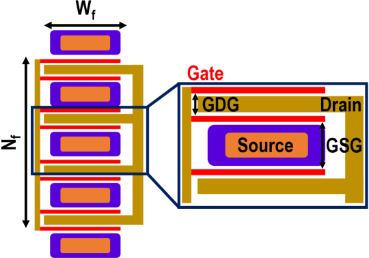
In the context of PA device sizing, we have one operating parameter, , and five design variables (i.e., factors we have control over), specifically , , , , and . Table 1 outlines the operating parameter range (with linear spacing) corresponding to utilized in the context of PA device sizing, representing the factor chosen by the adversary to assess the worst-case scenario for each objective. Here, the range was chosen to be across a reasonable bias range where the devices might be typically operated in [G+22, BSG+19, SBF+19]. It translates to an range of mA/mm. In practice, the range for robust optimization is primarily driven by the application, and it is up to the user to carefully choose a reasonable range to ensure no additional performance is unnecessarily “thrown away.” Furthermore, Table 2 summarizes the type, range, and number of points (with linear spacing) for these five design variables, representing a total of 672 designs. In addition, Fig. 1 showcases a qualitative layout of a HEMT, visually showing the physical representation of the design variables used.
| Parameter | Range | Step |
|---|---|---|
| 0.1 |
| Variable | Type | Range | Points |
|---|---|---|---|
| Float | 4 | ||
| Float | 7 | ||
| Even Integer | 4 | ||
| Float | 2 | ||
| Float | 3 |
With regard to the objectives used for PA device sizing, we primarily considered modulation performance metrics as they are a better representation of system-level performance [MMS+23]. Interested readers may refer to [MMS+23] for a more detailed comparison of various metrics used to quantify GaN HEMT devices in the context of PA applications.
The modulated performance was quantified by a 5G new radio (NR) uplink CP-OFDM 64-QAM modulation scheme, which was generated using the virtual test bench (VTB) in Keysight EDA ADS. In this modulation scheme, the maximum allowable EVM is 8%, and the maximum allowable ACPR is dBc, in accordance with the standards for NR devices [3GP19]. The modulated signal was then utilized to characterize signal distortion, employing methods such as the compact test signal and distortion EVM [VSTK19]. This approach was designed to expedite simulation time while maintaining high accuracy, which is necessary to simulate the 672 designs.
In our approach, we have implemented self-heating functionality to capture electro-thermal effects accurately, which are inherently layout-dependent. This was done using Keysight EDA’s Electro-Thermal simulator to calibrate self-heating within the MACOM HEMT model for the various geometries. Similarly, each of the device’s optimal load-pull impedances that minimized Gain compression while providing high Gain and PAE was extracted for the 672 designs. To focus solely on the contribution of the fundamental harmonic, the terminations for all other harmonics (i.e., second, third, fourth, and fifth harmonics) were “opened” (i.e., set to a high value) accordingly.
A frequency of 30 GHz was selected, primarily aiming to align with the 5G frequency bands, i.e., the employed modulation scheme is a Cyclic Prefix-Orthogonal Frequency Division Multiplexing (CP-OFDM) 64-QAM signal, with a center frequency () of 30 GHz and a bandwidth (BW) of 10 MHz. The finger width in the designs that were taken into consideration was optimized up to 100 since, beyond this value, there is a noticeable decline in the device’s Gain. Given that EVM is usually the limiting factor in PA design under modulated conditions, the objectives, namely , , and the modulated average junction temperature () were extracted at a fixed EVM of 8%. This EVM value represents the highest tolerable EVM for a 64-QAM modulation scheme. On the other hand, ACPR and Gain are used as constraints instead of objectives, where any design with an ACPR of more than dBc (i.e., ACPR requirement for NR devices [3GP19]) or less than 7 dB of Gain is deemed infeasible.
3.2 LNA Device Sizing Design Variables and Objectives
The operating parameter and design variables used for LNA device sizing are the same as those used for PA device sizing. However, the operating parameter range differs since the application targets low-noise amplification [Mea23]. The number of designs has also significantly increased, totaling 2,352. This is a greater number because simulating small-signal objectives in the context of LNA design is generally faster. Table 3 outlines the operating parameter range (with linear spacing) corresponding to the used in LNA device sizing, which translates to mA/mm. Additionally, Table 4 summarizes the type, range, and number of points (with linear spacing) for the five design variables used for LNA device sizing.
| Parameter | Range | Step |
|---|---|---|
| 0.1 |
| Variable | Type | Range | Points |
|---|---|---|---|
| Float | [16, 28] | 7 | |
| Float | [25, 100] | 7 | |
| Even Integer | [2, 8] | 4 | |
| Float | [22, 52] | 3 | |
| Float | [33, 78] | 4 |
Unlike in PA device sizing, self-heating is not included in the simulations, which significantly reduces computation time and increases the number of designs. A frequency of 30 GHz was selected once again, targeting 5G frequency bands. We primarily considered four objectives: , Gain (at 30 GHz), and minimum noise figure (, at 30 GHz).
3.3 Optimal Device Sizing for PAs
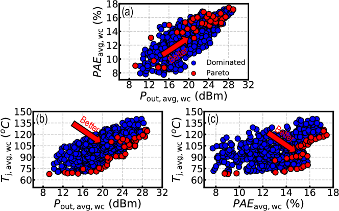
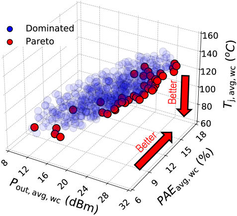
To find optimal device sizes in the context of PA applications, 4,704 SPICE simulations are done, accounting for 672 device designs and seven different bias conditions. On average, each simulation takes approximately three minutes, resulting in approximately 9.8 days of simulation time to solely simulate these device designs under modulated conditions. After considering the worst-case performance for each objective along with the imposed constraints (i.e., and Gain 7 dB) across the 7 bias conditions (to account for robustness), this number reduces to 528 robust designs, where 144 points are deemed infeasible. From these robust designs, the robust Pareto optimal designs are then found by maximizing and while minimizing . This results in a total of 39 robust Pareto optimal designs. Fig. 2 showcases the 2D cross-sections of the optimal trade-off surface for various objectives, highlighting the Pareto optimal designs in red and the dominated designs in blue. In a similar manner, Fig. 3 shows the optimal trade-off surface, where the Pareto optimal designs are highlighted in red while the dominated designs are highlighted in blue. Based on these results, it can be seen that a variety of optimal designs with different trade-offs can be chosen. For example, if is a top priority, then a robust Pareto optimal design can be selected with the desired value at the expense of a higher , which is generally the case since a larger device is needed.
3.4 Optimal Device Sizing for LNAs
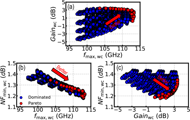
The optimal device sizes for LNAs are found using a procedure similar to that used for the sizing of PAs. However, 16,464 SPICE simulations were performed, accounting for 2,352 device designs and seven bias conditions. These simulations were much faster, taking at most one hour to complete, given that these are small-signal simulations. When considering the worst-case performance for each objective, the number of robust designs was reduced to 2,352. The robust Pareto optimal designs were then found by maximizing and Gain, and minimizing , resulting in a total of 60 robust Pareto optimal designs. These results are summarized in the 2-D cross-sections of the optimal trade-off surface for the three objectives in Fig. 4, where the Pareto optimal and the dominated points are highlighted in red and blue, respectively. The optimal trade-off surface is also shown in Fig. 5 with the Pareto optimal designs highlighted in red and the dominated designs in blue.
4 Derivative-free Optimization in Device Sizing
In a variety of engineering optimization problems, the objective functions or constraints generally involve complex, time-intensive simulations, which is the case in the present work. In some instances, the objective function might not be differentiable or is too computationally expensive to differentiate. An elegant solution in such scenarios is to resort to derivative-free optimization, a black-box approach that does not require gradient information about the objective function [KCK11, CSV09, RS13, LMW19]. Derivative-free optimization particularly shines in the context of ML, more specifically, in hyperparameter tuning, where the objective is to find the set of hyperparameters that yields the best model performance [KGG+18, MBK+22, BKE+15, ASY+19]. There are numerous open-source HPO frameworks that employ DFO methods, which include Autotune [KGG+18], HOLA [MBK+22], Hyperopt [BKE+15], and Optuna [ASY+19], to name a few. In this work, we have chosen to use HOLA. Although the selection of a specific HPO framework is not critical for our task, HOLA offers distinct advantages when addressing multiple objectives. It minimizes an overall scalar cost function by combining multiple objectives with a target-priority-limit scalarizer, streamlining the process of selecting a Pareto design.
With respect to device sizing optimization, we are presently dealing with five design variables, and our objectives for PA optimization are to maximize and while minimizing . For LNAs, we are primarily interested in maximizing and Gain, and minimizing . Resource-intensive simulations are needed to compute these objectives, particularly for simulations requiring a modulated stimulus (e.g., a 64-QAM signal). If we were to consider every possible combination of design variables, the computation time would become prohibitively expensive and time-consuming, leading to the curse of dimensionality. By using a DFO method, particularly a hyper-parameter optimizer like HOLA, the optimization process is steered toward regions in the design space where robust Pareto designs are likely to be found. It also drastically reduces the number of required simulations, reducing simulation time and computational power. Moreover, the optimization problem can be quickly adjusted if the design objectives or constraints change. However, one drawback of this method is that we do not know if a global optimal design was achieved. This is because DFO methods employ stochastic or heuristic approaches for search space sampling, which may not fully traverse the search space, potentially resulting in convergence to local minima.
Our proposed method is broadly applicable to other engineering applications that require optimizing one or multiple objectives with various design variables. Some examples include compact model parameter extraction [MIW+24] or device TCAD simulations. We have demonstrated its efficacy in the context of device sizing, where carrying out exhaustive simulations ensures the certainty of the results. This approach allows us to confidently identify the global optimum in design. However, it is important to highlight that, in practical settings, conducting exhaustive simulations is often impractical. The primary advantage of our method is that it can lead to the identification of optimal or near-optimal device designs, achieving the set objectives with far fewer simulations than a full grid search would require.
4.1 Derivative-free Optimization Using HOLA
HOLA considers a vector within a subset of to represent the selected hyperparameters from a feasible set . The -th element of vector is given by . In the context of the present work, denotes a vector of the design variables of interest (e.g., , , , etc.). As previously defined, represents the vector-valued objective under worst-case conditions, . Each objective has a desired direction of optimization, meaning some are to be maximized and others minimized. The different choices of hyperparameters or design variables are compared by scalarizing the objectives into a singular cost function, , which we want to minimize. By convention, designates an unacceptable hyperparameter vector. The transformation is realized through a target-limit-priority scalarization function , which maps the vector of objectives to the real numbers. This can expressed as . In essence, represents a traditional weighted sum of objectives.
The target-priority-limit scalarizer is separable and can be represented as:
| (2) |
where each is characterized by three parameters: a target value , a priority , and a limit . For an objective function that we want to minimize, the requirement is that , and the function is defined as:
| (3) |
The scalarizer is designed to be non-negative (), achieving its minimum of zero when the objective is at or below the target value. When the objective value exceeds the target and stays below the limit, will increase in a linear fashion, directly proportional to . If exceeds the limit, it incurs an infinite penalty via the scalarizer function, i.e., . Essentially, the target represents the ideal or satisfactory performance level, the limit denotes the maximum allowable value, and the priority dictates the gradient between these bounds. In the case of an objective function we want to maximize, the inequality is inverted by setting and reversing the definition of .
Having already established the scalarizer function , the goal of HOLA is then to identify an optimal vector within that minimizes through simulations. We seek to solve the optimization problem:
| (4) |
In terms of sampling, a hybrid approach was employed, given the limitations of random sampling. The procedure is first started with random sampling, and subsequently, the sampling strategy is enhanced by incorporating Sobol sequences. This hybrid approach allows for a more systematic exploration of the hyperparameter space, which potentially improves the algorithm’s performance. Once a baseline of hyperparameter values is established, a threshold is introduced. Beyond this threshold, HOLA employs a learned model designed to identify the most promising hyperparameter values with greater efficacy. A Gaussian Mixture Model (GMM) is then used to collect new hyperparameter values and concurrently present the findings [MBK+22].
At its core, HOLA begins by exploring a wide spectrum of promising hyperparameter values in order to identify regions in the hyperparameter space with the most potential. Subsequently, the GMM is tailored to align with the top 20–30% best-performing hyperparameter samples observed thus far. This allows the GMM to progressively detect and adjust to the distribution of best-performing hyperparameter values. As more samples are collected, the GMM’s precision is enhanced, suggesting increasingly superior hyperparameter samples.
4.2 HOLA Simulations for Optimal Device Sizing of PAs
We resort to HOLA primarily to recover the robust Pareto optimal designs. Doing so provides a better understanding of the trade-off space for more informed decision-making. Most importantly, HOLA allows us to find near-optimal or optimal designs in a relatively small number of trials as opposed to performing a more comprehensive search.
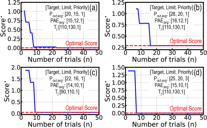
This process begins by first setting the attributes of the design variables (or hyperparameters). We closely follow the description provided in Table 2 for the type, range, and number of points (given by a finite set of values) for optimal device sizing of PAs. Four different scenarios are then considered, corresponding to various targets, priorities, and limits for the three objectives , , and . The optimal score is then calculated for these four scenarios based on the definition of , which is given by (3) and represents the lowest possible score that can be obtained based on the given targets, priorities, and limits. For each of the four scenarios, we run a simulation in HOLA with 50 trials, and we note down what is the best score found to date, which we denote as Score⋆. The results are summarized in Table LABEL:tab::HOLA_pa and in Fig. 6, where Score⋆ is shown for various number of trials () along with the corresponding target, limit, priority, and optimal score of three objectives, i.e., //. Here, each cell achieving the optimal score is highlighted in green.
Based on these results, we found that the optimal score is reached in 25 trials, which corresponds to searching less than 4 of the 672 robust designs. This outcome highlights the effectiveness of the derivative-free approach in identifying near-optimal or optimal designs with significantly fewer trials, as opposed to an exhaustive search among all 672 designs. Ultimately, this method drastically reduces simulation time from 9.8 days to just a matter of seconds.
4.3 HOLA Simulations for Optimal Device Sizing of LNAs
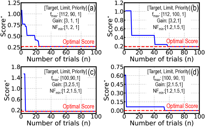
Similar to what was done for PAs, we resort once again to HOLA, but this time, a much larger number of designs is used (i.e., 2,352 robust LNA designs as opposed to 672). We consider four distinct scenarios with different targets, limits, and priorities for the three objectives, namely , Gain, and . The optimal score is calculated for these four scenarios, and a simulation with 100 trials is performed in HOLA. The results of the 100-trial simulation are summarized in Table 6 and in Fig. 7 along with the corresponding target, limit, priority, and optimal score of three objectives /Gain/. These results showcase HOLA’s effectiveness in finding near-optimal or optimal designs in less than 60 trials, corresponding to less than 2.6 of the total number of robust designs. We observe that as the number of designs increases, HOLA’s capabilities become more and more useful in finding good designs in fewer trials with respect to the total number of designs.
In this particular example, HOLA evaluated less than 60 designs instead of going through all 2,352 designs. This approach is highly beneficial in problems with larger design spaces, such as in device-level TCAD simulations, which involve a greater number of design variables and lead to a vast number of design possibilities (in the order of millions). Despite the uncertainty of not knowing if the best possible (global) design has been achieved, there is a high likelihood that a near-optimal design has been identified with just a fraction of the simulations that a full-grid search would require.
| Target | Limit | Priority | Optimal Score | Score⋆ | |||||
|---|---|---|---|---|---|---|---|---|---|
| 20/15/110 | 15/12/130 | 1/1/1 | 0 | 0.025 | 0.025 | 0 | 0 | 0 | |
| 28/16/110 | 20/12/130 | 1/1/1 | 0.289 | 0.783 | 0.289 | 0.289 | 0.289 | 0.289 | 0.289 |
| 22/14/90 | 16/10/110 | 1/1/1 | 0.049 | 0.049 | 0.049 | 0.049 | 0.049 | 0.049 | |
| 25/15/110 | 20/10/130 | 3/1/1 | 0 | 0 | 0 | 0 | 0 | 0 | |
| Target | Limit | Priority | Optimal Score | Score⋆ | |||||
|---|---|---|---|---|---|---|---|---|---|
| 112/3/1 | 90/1/2 | 1/1/1 | 0.265 | 1.081 | 0.412 | 0.265 | 0.265 | 0.265 | 0.265 |
| 112/3/1.2 | 100/2/1.5 | 1/1/1 | 0.448 | 0.448 | 0.189 | 0.189 | 0.189 | 0.189 | |
| 100/3/1.2 | 90/2.5/1 | 1/1/1 | 0.154 | 0.154 | 0.154 | 0.154 | 0.154 | 0.154 | |
| 100/2/1.2 | 90/1.5/1.5 | 1/1/1 | 0 | 0.608 | 0.063 | 0.063 | 0 | 0 | 0 |
5 Conclusion
In this work, we have shown a robust Pareto design approach for sizing GaN HEMTs in the context of both PA and LNA settings. Five key design variables were addressed to target three different objectives. The device designs were assessed based on their worst-case performance over various values of . A derivative-free optimization method was then used to identify robust Pareto optimal designs to enhance our understanding of the trade-offs involved. While our DFO method does not guarantee a globally optimal design, it found Pareto optimal designs much faster than if we did a full grid search. This approach provides a practical solution for sizing GaN HEMTs in 5G technology and is broadly applicable to various engineering design scenarios where multiple design variables and one or more objectives are at stake. The code used for this work can be found in our GitHub repository.111https://github.com/rafapm/robust_pareto_design
Acknowledgements
This work was supported in part by the Stanford Graduate Fellowship (SGF).
References
- [3GP19] 3GPP. NR: Base Station (BS) Radio Transmission and Reception. https://www.3gpp.org/, Jan 2019. 3GPP TS 38.104.
- [AEMREH23] A. Amar, R. El Maani, B. Radi, and A. El Hami. Multi-objective optimization of the high electron mobility transistor. Int. J. Simul. Multidisci. Des. Optim., 14:16, Dec. 2023.
- [ASY+19] T. Akiba, S. Sano, T. Yanase, T. Ohta, and M. Koyama. Optuna: A next-generation hyperparameter optimization framework. In Proc. 25th ACM SIGKDD Int. Conf. Knowl. Discovery Data Mining, pages 2623–2631. ACM, 2019.
- [BJK+24] S. Boyd, K. Johansson, R. Kahn, P. Schiele, and T. Schmelzer. Markowitz Portfolio Construction at Seventy. arXiv:2401.05080, 2024.
- [BKE+15] J. Bergstra, B. Komer, C. Eliasmith, D. Yamins, and D. D. Cox. Hyperopt: A python library for model selection and hyperparameter optimization. Comput. Sci. Discovery, 8(1):014008, 2015.
- [BS07] H. Beyer and B. Sendhoff. Robust optimization—a comprehensive survey. Comput. Methods Appl. Mech. Eng., 196(33-34):3190–3218, 2007.
- [BSG+19] K. M. Bothe, B. Schmukler, S. Ganguly, T. Alcorn, J. Gao, C. Hardiman, E. Jones, D. Namishia, F. Radulescu, J. Barner, J. Fisher, D. Gajewski, S. Sheppard, and J. Milligan. Optically-Defined 150nm, 28-V GaN HEMT Process for Ka-Band. In Proceedings of the CS MANTECH Conference, Minneapolis, MN, USA, 2019. CS MANTECH.
- [BTGN09] A. Ben-Tal, L. El Ghaoui, and A. Nemirovski. Robust Optimization, volume 28. Princeton University Press, 2009.
- [BV04] S. Boyd and L. Vandenberghe. Convex Optimization. Cambridge University Press, 2004.
- [CSV09] A. R. Conn, K. Scheinberg, and L. N. Vicente. Introduction to Derivative-Free Optimization, volume 8. SIAM, Philadelphia, PA, USA, 2009.
- [DENB05] C.H. Doan, S. Emami, A.M. Niknejad, and R.W. Brodersen. Millimeter-wave CMOS design. IEEE J. Solid-State Circuits, 40(1):144–155, 2005.
- [Fri44] H. T. Friis. Noise figures of radio receivers. Proc. IRE, 32(7):419–422, Jul. 1944.
- [G+22] S. Ganguly et al. DC and RF Reliability Assessment of 5G-MMW capable GaN HEMT Process (Invited). In Proc. IEEE Int. Rel. Phys. Symp. (IRPS), page 11, 2022.
- [GMT14] V. Gabrel, C. Murat, and A. Thiele. Recent advances in robust optimization: An overview. Eur. J. Oper. Res., 235(3):471–483, 2014.
- [Gon96] G. Gonzalez. Microwave Transistor Amplifiers (2nd Ed.): Analysis and Design. Prentice-Hall, Inc., USA, 1996.
- [GSS14] I. J. Goodfellow, J. Shlens, and C. Szegedy. Explaining and harnessing adversarial examples. arXiv:1412.6572, 2014.
- [KCK11] O. Kramer, D. E. Ciaurri, and S. Koziel. Derivative-free optimization. In Computational Optimization, Methods and Algorithms, pages 61–83. Berlin, Germany: Springer, 2011.
- [KGG+18] P. Koch, O. Golovidov, S. Gardner, B. Wujek, J. Griffin, and Y. Xu. Autotune: A derivative-free optimization framework for hyperparameter tuning. In Proc. ACM SIGKDD Conf. Knowl. Discov. Data Mining, page 443–452, 2018.
- [L+09] A. Leuther et al. Metamorphic HEMT technology for low-noise applications. In Proc. IEEE Int. Conf. Indium Phosph. Rel. Mater. (IPRM), pages 188–191, May 2009.
- [Lie76] C. A. Liechti. Microwave field-effect transistors. IEEE Trans. Microw. Theory Techn., 24:279–300, 1976.
- [Liu20] Y. Liu. Designing GaN on SiC MMIC power amplifiers using the Cree/Wolfspeed MWO PDK. In IEEE MTT-S Int. Microw. Symp. Dig., Jul. 2020.
- [LMW19] J. Larson, M. Menickelly, and S. M. Wild. Derivative-free optimization methods. Acta Numerica, 28:287–404, May 2019.
- [LZY+23] H. Lu, M. Zhang, L. Yang, B. Hou, R. P. Martinez, M. Mi, J. Du, L. Deng, M. Wu, S. Chowdhury, X. Ma, and Y. Hao. A Review of GaN RF Devices and Power Amplifiers for 5G Communication Applications. Fundamental Research, 2023.
- [MAC23] MACOM. RF Foundry, 2023. [Online; accessed 18-December-2023].
- [MBK+22] G. Maher, S. Boyd, M. Kochenderfer, C. Matache, A. Ulitsky, S. Yukhymuk, and L. Kopman. A Light-Weight Multi-Objective Asynchronous Hyper-Parameter Optimizer. arXiv:2202.07735, 2022.
- [Mea23] N. C. Miller et al. A Survey of GaN HEMT Technologies for Millimeter-Wave Low Noise Applications. IEEE J. Microw., 3(4):1134–1146, Oct. 2023.
- [MIW+24] R. P. Martinez, M. Iwamoto, K Woo, Z. Bian, R. Tinti, S. Boyd, and S. Chowdhury. Compact Model Parameter Extraction via Derivative-Free Optimization. arXiv:2406.16355, 2024.
- [MMS+23] R. P. Martinez, D. J. Munzer, B. Shankar, B. Murmann, and S. Chowdhury. Linearity Performance of Derivative Superposition in GaN HEMTs: A Device-to-Circuit Perspective. IEEE Trans. Electron Devices, 70(5):2247–2254, Mar. 2023.
- [MPW02] U. K. Mishra, P. Parikh, and Y.-F. Wu. AlGaN/GaN HEMTs-an overview of device operation and applications. Proc. IEEE, 90(6):1022–1031, Jun. 2002.
- [MSKW08] U. K. Mishra, L. Shen, T. E. Kazior, and Y-F. Wu. GaN-Based RF Power Devices and Amplifiers. Proc. IEEE, 96(2):287–305, Jan. 2008.
- [NP21] H. T. Nguyen and A. F. Peterson. Machine Learning for Automating the Design of Millimeter-Wave Baluns. IEEE Trans. Circuits Syst. I, Reg. Papers,, 68(6):2329–2340, Apr. 2021.
- [PMF+08] R. Pengelly, B. Millon, D. Farrell, B. Pribble, and S. Wood. Application of non-linear models in a range of challenging GaN HEMT power amplifier designs. In IEEE MTT-S Int. Microw. Symp. Dig., Jun. 2008.
- [Pos89] M. W. Pospieszalski. Modeling of noise parameters of MESFETs and MODFETs and their frequency and temperature dependence. IEEE Trans. Microw. Theory Techn., 37(9):1340–1350, Sep 1989.
- [PP13] R. Pengelly and B. Pribble. Intrinsic Cree GaN HEMT models allow more accurate waveform engineered PA designs. In Proc. ARMMS Conf., pages 1–31, Apr. 2013.
- [Raz11] B. Razavi. RF Microelectronics. Prentice Hall Press, USA, 2nd edition, 2011.
- [RS13] L. M. Rios and N. V. Sahinidis. Derivative-free optimization: A review of algorithms and comparison of software implementations. J. Global Optimiz., 56(3):1247–1293, 2013.
- [SBF+19] B. Schmukler, J. Barner, J. Fisher, D. A. Gajewski, S. T. Sheppard, J. W. Milligan, K. M. Bothe, S. Ganguly, T. Alcorn, J. Gao, C. Hardiman, E. Jones, D. Namishia, and F. Radulescu. A high efficiency, Ka-band, GaN-on-SiC MMIC with low compression. In Proc. IEEE BiCMOS and Compound Semiconductor Integrated Circuits and Technology Symposium (BCICTS), pages 1–4, November 2019.
- [VSTK19] J. Verspecht, A. Stav, J.-P. Teyssier, and S. Kusano. Characterizing Amplifier Modulation Distortion Using a Vector Network Analyzer. In Prof. 93rd ARFTG Conf. Dig., pages 1–4, Jun. 2019.
- [WBN+24] K. Woo, Z. Bian, M. Noshin, R. P. Martinez, M. Malakoutian, B. Shankar, and S. Chowdhury. From Wide to Ultrawide-Bandgap Semiconductors for High Power and High Frequency Electronic Devices. J. Phys.: Mater, 2024.
- [WG21] T. Wu and J. Guo. Multiobjective Design of 2-D-Material-Based Field-Effect Transistors With Machine Learning Methods. IEEE Trans. Electron Devices, 68(11):5476–5482, Jun. 2021.
- [XGC+22] H. Xu, W. Gan, L. Cao, C. Yang, J. Wu, M. Zhou, H. Qu, S. Zhang, H. Yin, and Z. Wu. A Machine Learning Approach for Optimization of Channel Geometry and Source/Drain Doping Profile of Stacked Nanosheet Transistors. IEEE Trans. Electron Devices, 69(7):3568–3574, May 2022.