Probing Yu-Shiba-Rusinov state via quantum noise and noise
Tusaradri Mohapatra
Sachiraj Mishra
Colin Benjamin
colin.nano@gmail.comSchool of Physical Sciences, National Institute of Science Education and Research, HBNI, Jatni-752050, India
Homi Bhabha National Institute, Training School Complex, AnushaktiNagar, Mumbai, 400094, India
Abstract
Recent attention has been drawn to temperature gradient generated noise at vanishing charge current. This
study delves into examining the properties of spin-polarised noise in conjunction with -shot noise, -thermal noise, and quantum noise (again both shot and thermal noise) in a one-dimensional (1D) structure comprising metal/spin-flipper/metal/insulator/superconductor junction to probe Yu-Shiba-Rusinov (YSR) bound states. YSR bound states, which are localized states within the superconducting gap of a superconductor are induced by a magnetic impurity acting as a spin-flipper. A YSR bound state should be distinguished from a Majorana bound state (MBS), which too can occur due to interaction with magnetic impurities, e.g., magnetic adatoms on superconductors, and this can lead to false positives in detecting MBS. Clarifying this by providing a unique signature for the YSR-bound state is the main aim of this work. In this paper, we show that YSR bound states can be effectively probed using quantum noise and the recently discovered noise, with a focus on especially spin transport. We see that the spin noise is a superior tool compared to the charge noise as a probe for YSR bound states. Additionally, our analysis of quantum noise reveals that similar to noise, spin quantum noise is more effective than charge quantum noise in detecting YSR bound states.
I Introduction
Quantum noise provides a valuable tool in the understanding of quantum statistics, non-Abelian statistics of anyons in fractional quantum Hall setups [1, 2, 3, 4, 5, 6]. Additionally, it is used to determine the effective fractional charge in fractional quantum Hall setups [7, 8, 9, 10] and the cooper pair’s charge in a metal-superconductor junction [11, 12, 13]. A recent study shows that it can also be utilized to distinguish different edge mode transport such as chiral, helical, and trivial helical edge modes. [14]. Very recent area of intense research in mesoscopic physics is quantum noise, borne by both theoretical predictions [15, 16, 17] and experimental observations [18, 19, 20]. In contrast to quantum noise, noise arises even without a net charge current in the system, provided there is a finite temperature gradient.
Unintentional temperature differences in experimental measurements can sometimes result in abrupt noise, which may be mistaken for noise stemming from other subtle effects [18]. noise proves effective in examining such occurrences, given its versatility without specific design constraints [19]. Recent studies have suggested that the charge shot noise contribution is positive for fermions, while for bosons, it can be either positive or negative [21].
Spin-flip scattering occurs when an incoming electron interacts with a spin flipper at the interface. Spin current holds significant relevance in spintronics [22], particularly within superconducting junctions, to investigate both spin and charge transport. A YSR bound state forms when magnetic impurity spin interacts with the Cooper pairs of the superconductor, leading to the formation of bound states within the superconducting energy gap [23, 24, 25]. Superconductors, particularly conventional s-wave type, exhibit a fascinating phenomenon when encountering magnetic impurities. These impurities can form unique bound states within the superconducting gap. This discovery, made independently by Yu, Shiba, and Rusinov [23, 24, 25], laid the foundation for our understanding of YSR states. The emergence of YSR states arises from the interaction between the impurity’s spin and the electron-like or hole-like quasiparticles that are reflected back by the superconductor through a process known as Andreev reflection.A YSR bound state should be distinguished from a Majorana
bound state (MBS) which too can occur due to interaction with magnetic impurities,
e.g., magnetic adatoms on superconductors [26, 27, 28] and this can lead to false positives
in detecting MBS. Clarifying this by providing an unique signature for YSR bound state
is the main aim of this work. Experimental verification of YSR bound states has been achieved in recent years using scanning tunneling spectroscopy and atomic scale shot noise spectroscopy [29, 30]. In this work, we demonstrate that YSR bound states can be effectively probed using quantum noise and the recently discovered noise, with a focus on both charge and spin transport mechanisms.
Our study focuses on the YSR bound states induced by magnetic impurities that act as a spin-flipper in a superconducting junction at vanishing charge or spin current via charge noise () or spin noise () noise and quantum charge and spin noise. We also analyze the corresponding contributions from charge (spin) -shot noise () and charge (spin) -thermal noise ().
We consider a finite temperature difference between the left normal metal and the superconductor, along with a finite applied voltage bias (as detailed in subsections II.2).
Differential charge conductance exhibits a zero-bias peak in the presence of magnetic impurities, caused by the merging of two YSR-bound states inside the superconducting gap. This occurs for specific values of barrier strength and exchange interaction strength.
The charge (spin) thermal noise () exhibits a peak at one barrier strength value corresponding to one YSR peak, whereas the charge (spin) -shot noise () displays dips at both barrier strength values, where YSR peaks occur. Charge (spin) quantum noise also shows a peak at only one of the barrier strength values. Consequently, the charge (spin) shot noise () is a superior tool for probing YSR bound states in the presence of a magnetic impurity.
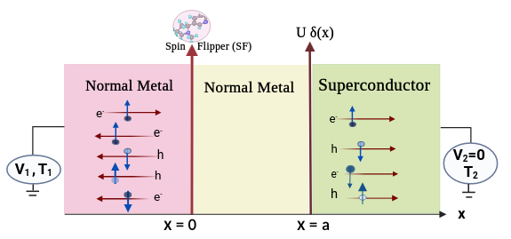
Figure 1: Schematic representation of 1D NsfNIS junction, with a magnetic impurity which acts as a spin-flipper at and potential at .
This paper is structured as follows: Section II provides an overview of charge transport, which focuses on the calculation of spin-polarized scattering amplitudes in a NsfNIS junction. Subsequently, we discuss and calculate spin-polarized quantum noise and charge (spin) noise at a finite temperature gradient. Section III delves into the YSR bound state and its signature via conductance, followed by an examination of spin-polarized noise, noise. Section IV analyzes the results of and quantum noise and discusses how they can detect YSR-bound states, which results are summarized in Tables II and III. Section V concludes this paper with a discussion on the experimental realization of our work. The derivation of charge (spin) current in a NsfNIS junction is given in Appendix A, while Appendix B presents the calculation of spin-polarized quantum noise in a NsfNIS junction. Appendix C.1 contains the derivation of charge (spin) thermovoltage necessary for calculating charge (spin) noise, and Appendix C.2 presents the derivation of spin-polarised charge (spin) noise, including the derivation of charge (spin) and noise contributions. The Mathematica code to calculate charge (spin) thermovoltage and noise is given in Github [31].
II Theory
Employing the Bogoliubov-de Gennes (BDG) formalism, the Hamiltonian for a NsfNIS junction, as detailed in a prior work [32], is represented as follows:
(1)
where, , with being the momentum, denoting the fermi energy, representing the effective mass, denoting the strength of the delta potential, being the Heaviside theta function, being the superconducting gap (Ref. [33]), and representing the relative strength of the exchange interaction between the electron spin and the magnetic impurity spin . The exchange interaction in is expressed as:
(2)
here, the raising and lowering electron spin’s (spin-flipper’s spin) operator are represented as (). Additionally, represent the components of the electron’s spin operator, while represent the corresponding components of spin-flipper’s spin operator.
The wavefunctions in different regions of NsfNIS junction for a spin-up electron incident from left normal metal are given as,
(3)
The wavefunctions in different regions of NsfNIS junction for spin-down electron is incident from left normal metal are given as,
(4)
(37)
where denotes the eigenfunction of , i.e., , where denotes the spin magnetic moment. represent the wave-vectors in the normal metal for electrons and holes, given by , where represents the excitation energy of the electron. Moreover, wave-vectors for electron-like (hole-like) quasiparticles in the superconductor are , while the coherence factors are in Eq. (37).
The electron’s spin operator denoted as and spin-flipper’s spin operator denoted as operating on the spin-up electron spinor [34, 35, 32] and the spin-flipper eigen function gives,
(50)
and acting on the down-spin electron spinor and the spin-flipper eigen function gives,
(63)
Furthermore, acting on the spin-up hole spinor and the spin-flipper eigen function gives,
(76)
acting on the spin-down hole spinor and the spin-flipper eigen function gives,
(89)
where , represent the probabilities of spin-flip for electrons with up-spin and down-spin incident on the left normal metal, where denotes the spin of the spin-flipper, with the value of ranging from to .
The boundary conditions in a NsfNIS junction at the interface are,
(90)
and at the interface in a NsfNIS junction are,
(91)
Incorporating Eqs. (3) (or (4)) into Eqs. (90) and (91), we get scattering amplitudes for spin-up (or spin-down) incident electron, where the barrier strength is and the exchange interaction strength is , with being the Fermi wave vector.
In a NsfNIS junction, an incident spin-up electron can undergo four possible reflection processes at the interface. Firstly, the electron may undergo reflection without spin-flip, where it is reflected as an electron with the same spin. Alternatively, it may experience Andreev reflection, reflecting the electron as a hole with an opposite spin. Moreover, the electron could undergo reflection with a spin-flip, resulting in its reflection as an electron with a flipped spin. Lastly, Andreev reflection with spin-flip may occur, causing the electron to be reflected as a hole with the same spin.
The Andreev reflection with and without spin-flip are characterized by the amplitudes and . In contrast, the normal reflection with and without spin-flip are denoted by the amplitudes and .
Furthermore, the transmission amplitudes with (without) spin-flip are given as: (or, ), which represents the transmission amplitude of an up-spin electron transmitted as a down-spin (or, up-spin) electron, and (or, ) represents the transmission amplitude of an up-spin electron transmitted as a up-spin (or, down-spin) hole, and their respective probabilities are given as , , , , , and , . The coefficients , and are introduced to ensure the conservation of the probability current, as explained in Ref. [36].
Figure 2: This box illustrates the different spin configurations that arise when an electron (with spin or ) interacts with a spin-flipper. The spin-flipper’s spin state () can be either aligned () or anti-aligned () with the electron’s spin. The spin-flip probabilities for up-spin incident electron and down-spin incident electron are denoted as and , respectively.
When the time between electron collisions (electron’s elastic scattering time, ) is significantly longer than the spin-flipper’s relaxation time (), i.e., , the spin-flipper rapidly flips its spin before encountering the next incoming electron, as illustrated in Fig. 2. This rapid relaxation implies that the magnetic moment () for spin associated with a particular spin of the spin-flipper () fluctuates [37]. To accurately calculate any transport property, we take the average over all possible values of . We consider four scenarios based on the incident electron’s spin (up or down) and the spin-flipper’s configuration (aligned or anti-aligned with the incident electron’s spin). Four possible scenarios are an up-spin incident electron interacting with spin-flipper with spin is denoted as spin-configuration 1, or with is denoted as spin-configuration 2. Similarly, an electron with a down-spin incident from the left side of the normal metal interacting with spin-flipper at interface for is denoted as spin-configuration 3 and scenario with for is represented as spin-configuration 4, see Fig. 2.
Next, we discuss the charge current, spin-polarised quantum noise, and charge noise in a NsfNIS junction.
II.1 Current and spin-polarised quantum noise
For a NsfNIS junction,the average spin-polarised current in contact is [38, 2],
(92)
with for electron (hole). , with indices refer to left normal metal and superconductor, and denote electron or hole (see, Appendix A) with , , . () represents the creation (annihilation) operators for particle () at contact () with spin . The expectation value [1] simplifies to , wherein the Fermi function is independent of spin, with being the Fermi function in contact for particle , with for electron and for hole, is Boltzmann constant. represents the temperature and denotes the applied voltage bias at contact .
In our work, represents the temperature of normal metal , and represents the temperature of the superconductor with . The temperature difference is higher than the average, i.e., . In our work, we have considered and . For finite voltage bias, the voltage in normal metal () is finite, i.e., , and the superconductor is grounded, i.e., , see Fig. 1.
In the normal metal , Fermi function for the electron is , and for the hole is . In the superconductor (), Fermi function for electron-like quasiparticles is same as Fermi function for hole-like quasiparticles at , i.e., .
The average charge current [34, 35, 32] in the left normal metal () of the NsfNIS junction can be written as,
where , see Appendix A. Charge conductance in a NsfNIS junction at finite bias voltage (, ) can be expressed as , where .
The mean spin current [34, 35, 32] in can be written as,
(94)
where .
The current-current correlation at the same contact, i.e., at is the quantum noise-auto correlation. Spin polarised quantum noise in between charge carriers with spin and at different times and is defined as with [2]. The charge quantum noise auto-correlation at zero frequency [39] for charge current can be written as,
(95)
while the spin quantum noise auto-correlation at zero frequency for spin current is
(96)
where, the spin-polarised quantum noise-auto correlation at zero frequency in NsfNIS junction [38, 40] for is given as
(97)
where for electron (hole).
where, and , are the sum of the scattering probabilities for noise and noise contributions and their detailed expressions are given in Eqs. (110) and (108) of Appendix B. Here, and are the spin-polarized thermal and shot noise-like contributions, respectively, and they are given as
(98)
for . The total charge (spin) thermal and shot noise-like contributions are denoted as and are given as
(99)
II.2 Spin polarised noise
The quantum noise arising from a non-equilibrium temperature gradient in the absence of net charge current is termed as charge noise [15, 16, 17, 18, 19, 37]. We denote the charge noise is denoted as in this paper. One can calculate from (see Eq. (95)) at zero average charge current and by substituting the applied voltage bias by the charge thermovoltage [17, 37]. The expression for is given in Eq. (C3). has been calculated numerically in Mathematica (see Github [31]). Also, one can see Appendix C for the theory. Similarly, one can also calculate the spin noise, denoted as from (see Eq. (96)) at zero average spin current, i.e., and by substituting the applied voltage bias by the spin thermovoltage [37]. Similar to , can be calculated numerically in Mathematica (see Github [31]) and also see Appendix C for the theory.
comprises two contributions: thermal noise-like contributions represented as and shot noise-like contribution represented as . can be calculated from (see Eq. (99)) at zero average charge current (). Similarly, one can also calculate from (see Eq. (99)) at zero average spin current ().
The average charge current can be calculated by performing the Taylor series expansion of the Fermi-Dirac distributions and in a power series of and their difference after the expansion up to first order in is given as (see, Eq. (112) for the derivation following the Refs. [18, 15]
(100)
where, and . Using this expansion, charge thermovoltage can be calculated by equating (see Github [31] or Appendix C). The detailed derivation of thermovoltage () at vanishing charge current is given in Appendix C.1.
Following the same approach, we expand the Fermi functions within the expressions for shot noise () and thermal noise () like contribution to quantum noise in power series of for . Detailed derivations for these expansions are provided in Eqs. (115) and (118). Using these Fermi function expansions, and noise can be efficiently calculated numerically (see, Github [31] or Appendix C).
noise can be calculated from the quantum noise (see, Eq. (97)), by substituting the thermovoltage () in the voltage bias , for , and can be expressed as,
(101)
and the detailed derivation of noise is given in Appendix C.2 in Eqs. (C5) and (C6). is a function of reflection probabilities with and without spin-flip, with , and + .
The expressions for are derived in Appendix B, see Eq. (110).
noise is calculated from (see, Eq. (97)) by replacing the thermovoltage () in the applied voltage bias , for , and is written as (see Appendix C.2 for the derivation, Eq. (C8)),
(102)
where, is a function of reflection and transmission probabilities, which can be expressed as + and, + .
Further, expressions for for are derived in Appendix B in Eq. (B4).
Next, we discuss the origin of YSR bound states, along with results conductance, noise and quantum noise. of noise along with contributions from noise as a function of barrier strength in a NsfNIS junction.
III Results and Discussion
This section first delves into YSR bound states in a NsfNIS junction and the results for the charge conductance , noise at finite temperature gradient () (see Fig. 1) and quantum noise for . Also, we discuss the shot noise () and thermal noise () like contributions to . Similarly, in the case of quantum noise (at zero temperature gradient means ), we discuss its intermediate-bias regime (), high-bias regime (, shot noise limit) and low-bias regime (, thermal noise limit) This study considers niobium (Nb) as the superconducting material. Niobium has a superconducting gap of meV [33], and we consider the Fermi energy to be .
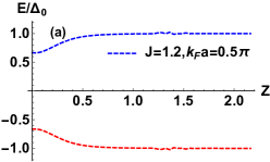
In Fig. 3, we show the YSR bound states in the NsfNIS junction. One can calculate the bound state energies by calculating the complex poles of the charge conductance [32] (see Github [31] for Mathematica code). The real parts of the poles of the conductance (see, Fig. 3) are the energies (), where these YSR peaks occur, while the imaginary part denotes the width of this peak. In Fig. 3, we plot the YSR bound states (real part of the energies) as a function of the barrier strength , where we observe there are two energy-bound states, while coalesce at two different barrier strength values and , where YSR conductance peaks result, see Fig. 4.
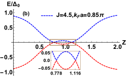
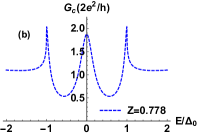
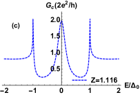
In Fig. 4, we plot charge conductance vs. energy for different barrier strength values , with , , and take the sum over . shows zero bias peaks at =0.778 and 1.116, which is the signature of YSR bound states within the superconducting gap ( see, Fig. 3). Apart from these two values, the zero-bias conductance peak is not observed at any other values. We have shown this for in Fig. 3(a). A magnetic impurity acting as a spin-flipper induces YSR-bound states within the superconducting gap, manifesting as a zero-bias peak. The zero bias conductance peak arises from the merging of two YSR bound states for specific values, i.e., , see, Fig. 3(b).
Figure 3: YSR bound states vs. barrier strength () , with spin-flipper parameters , , (a) , and (b) , .
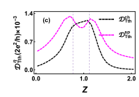
In Fig. 5(a), we plot noise, while in Fig. 5(b), we plot , whereas in Fig. 5(c), we show as a function of barrier strength (). We observe that the charge noise exhibits a peak at the barrier strength (), indicating the presence of one YSR bound state, where there is no such peak or dip at . However, spin noise shows peaks around both the barrier strengths () and (), indicating the two YSR bound states. Therefore, spin noise is effective tool rather than charge noise for detecting YSR bound states. In Figs. 5(b) and (c), we plot and respectively vs. barrier strength () for NsfNIS junction at finite bias voltage and finite temperature gradient. In Fig. 5(b), we observe that shows a dip at , whereas show dips at both values, i.e., at 0.778 and 1.116, where the zero-bias peaks occur. Thus, is again proved to be more effective than as a probe for YSR bound states. Similarly, in Fig. 5(c), noise shows peak at which corresponds to YSR peak, while noise shows peaks at
both values , where YSR peaks occur. Charge (spin) noise is the dominant contribution compared to charge (spin) noise, thus, noise shows almost the same behaviour as noise, see Figs 5(a) for noise and 5(c) for noise.
Figure 4: Differential charge conductance vs. , with , , (a) , (b) , and (c) .
Figure 5: (a) , (b) , and (c) vs. , with , , , , where in a NsfNIS junction.
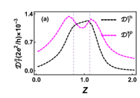
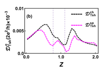
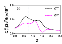
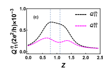
In Fig. 6, we plot the total charge (spin) quantum noise , along with the and noise, vs. barrier strength () at finite temperature , in three voltage bias limit, i.e., (i) at voltage bias (see, Fig. 6(a)), (ii) at high voltage bias regime (see, Fig. 6(b)) and (iii) for low voltage bias regime (see, Fig. 6(c)). In the first case (), noise does not show any signature of YSR bound states, while noise displays a dip at (see Fig. 6(a)). In the second case (), noise exhibits a dip near barrier strength value (see Fig. 6(b)), whereas shows a small dip, observed near with a peak near , indicating YSR bound states. In the third case (), noise cannot distinguish two YSR bound states (see, Fig. 6(c)), but shows a small dip around . Thus, charge quantum shot or spin thermal noise can not distinguish YSR bound states properly.
Figure 6: noise vs. for (a) (both shot noise and thermal noise contribute), (b) (shot noise regime) and (c) (thermal noise regime), with .
IV Analysis
Table 1: Comparison of noise with noise, where in a NsfNIS junction.
Here, we analyze the behaviour of finite temperature charge (spin) , and . We also analyze the results of quantum noise (), its high voltage-bias limit () and low voltage-bias limit (), as a function of barrier strength in a NsfNIS junction. In Table I, we give a comparison between both and . We see that in case of , thermal noise-like () contribution always dominates shot noise-like contribution (), whereas in case of quantum noise (), shot noise () dominates in the high-voltage bias limit, while thermal noise () dominates in the low-bias limit. In Table II, we have summarized the results of including the shot noise () and thermal noise () as regards their effectiveness in detecting YSR bound states. Similarly, in Table III, we summarize the results of , its high voltage-bias limit and low voltage-bias limit regarding their effectiveness in detecting YSR bound states.
Table 2: Nature of , and with the barrier strengths = 0.778 and 1.116 for the detection of YSR bound states for . () represents no peak or dip at the barrier strengths, which means no YSR-bound states can be probed.
Table 3: Nature of , and with the barrier strengths and for the detection of YSR bound states for . () represents no peak or dip at the barrier strengths, which means no YSR-bound states can be probed.
Fig. 5(a) shows that is more effective than in probing YSR bound states. We observe that exhibits peaks at both the barrier strengths and , where YSR bound states occur, whereas exhibits a peak only at thus detecting only one YSR bound state. Similarly, in Fig. 5(b), exhibits dip at both values, whereas shows a dip only at one value exactly at the same value where shows a peak. Therefore, is a better tool than to detect YSR-bound states. Similar to Fig. 5(a), exhibits peaks at those values of , see, Fig. 5(c), where YSR peaks occur, whereas shows a peak only at one of the values, thus again proving that is better than in detecting YSR-bound states. Thus, spin noise is far better than the charge noise in probing YSR bound states. These results are unique and can motivate experiments involving detection of YSR-bound states. Next, we analyze the quantum noise results of Fig. 6.
For voltage bias in the same range of average temperature meV, both noise and noise contribute to total noise, where . In the low bias voltage regime (), where meV) < meV), dominates noise (see, Fig. 6(c)). Thus, total noise shows similar behaviour as noise for low bias voltage. However, for high voltage bias regime (), where meV > meV, < noise (see, Fig. 6(b)). Thus, total noise shows similar behaviour as noise at high bias voltage. We observe that in the regime can detect both YSR bound states much more effectively than . Similarly, in the regimes and , provides a more effective way to detect YSR bound states.
V Experimental realization and Conclusion
Recently, researchers have experimentally measured noise arising from a finite temperature difference [18, 19, 20]. In our setup, i.e., metal-spin-flipper-metal-insulator--wave superconductor junction, we investigate and noise at finite temperature gradient and with finite voltage bias. For the superconductor, we opt for s-wave superconductor, i.e., Niobium (Nb) with critical temperature K and superconducting gap meV [33].
The spin flipper, acting as a magnetic impurity, lends itself to analysis akin to that of an Anderson impurity but distinct from a Kondo impurity, see, Ref. [34, 32, 41]. One approach involves employing a quantum dot comprising spin-paired electrons alongside an additional unpaired electron, which can be used as a magnetic impurity or spin flipper (Ref. [42]).
Here, we focus on noise, along with the contributions from and noise. We also focus on the quantum noise auto-correlation and its thermal noise-like contribution () and shot noise-like contribution (). We investigate these contributions for the barrier strength values in a NsfNIS junction to signify the YSR bound states below the superconducting gap. We find that for charge (spin) noise in NsfNIS junction, -shot noise is less than -thermal noise regardless of change in barrier strength . We observe that when the barrier strength is 0.778, does not show any signature of YSR bound states, where shows a peak at the same value of and this proves that is a better tool than , see Table II and Fig. 5(a). Similarly, at the same value , the shot noise-like contribution () and thermal noise-like contribution () do not show any evidence of YSR bound states, whereas their spin counterpart and provide clear evidence of YSR bound states by exhibiting dip and peak respectively (see, Figs. 5(b) and (c) and Table II). We also observe that at , , and shows signature of YSR bound states (see, Fig. 5 and Table II).
We have also focussed on quantum noise autocorrelation () in the intermediate voltage bias regime , their high voltage bias limit (), i.e., in the shot noise regime () and low voltage bias limit (), i.e., the thermal noise regime (). shows a peak or dip around for low bias voltage. Conversely, noise exhibits a peak only around , while noise exhibits a dip only around for high bias voltage, enabling the probing of one YSR bound state. This study gives valuable insights into the characteristics of spin-polarized and noise in superconducting junctions featuring a spin-flipper, which induces YSR bound states below the superconducting gap.
Additionally, it enhances our understanding of how the interplay between Andreev reflection and spin-flip scattering at finite temperature difference influences the behavior of and noise.
Appendix
The appendix is divided into three parts. The first section, Appendix A, covers the derivation of current due to charge and spin transport in normal metal () for a NsfNIS junction. Subsequently, in Appendix B, we calculate the expressions for quantum noise, which are spin-polarized. Next, we delve into the derivation of the charge (spin) thermovoltage in Appendix C.1 by equating charge (spin) current to zero, which is necessary for calculating the charge (spin) noise. Lastly, Appendix C.2 contains the derivation of total charge (spin) noise along with charge (spin) noise and charge noise in a NsfNIS junction.
Appendix A Spin-polarised average current
The expression for the spin-polarized average current () in the normal metal () is given by:
(103)
where for electron (hole). The term represents the matrix element, where indices label the normal metal () and superconductor () contacts respectively, and , denote electron or hole. The indices in Eq. (103), , , and denote the spin of the particle (electron or hole), specifically up-spin () or down-spin (). The operators and are the creation and annihilation operators, respectively, for particle in contact with spin , and for particle in contact with spin . The expectation value of the product of these operators simplifies to , where Fermi function is denoted as in contact (normal metal or superconductor) and for particles (electron or hole), and for electron (hole).
In our setup with a finite bias voltage (), the Fermi function for electrons in the normal metal is given by . In the superconductor at , Fermi functions for electron-like quasiparticles are the same as hole-like quasiparticles and represented as [38, 1].
Utilizing the properties , , , , and [36, 43, 1], the average charge current in (see, Refs. [36, 43]) can be simplified as,
(104)
where . Next, we calculate the spin-polarised quantum noise in a NsfNIS junction.
The mean spin current in the left normal metal (see, Refs. [36, 43]) as follows,
(105)
where .
Appendix B Spin-polarised quantum noise
Spin-polarised quantum noise is defined as the correlation between current in contact and current in contact with spin and [1, 3], such as , with , where is the spin-polarised current in lead with spin . Quantum noise power can be obtained by taking the Fourier transform of the quantum noise, expressed as . Zero frequency spin-polarised quantum noise ) [38], in a NsfNIS junction is,
(106)
where , and for electron (hole). Spin-polarised quantum noise auto-correlation () in a NsfNIS junction, is as follows,
(107)
Spin-polarised thermal noise contributions with terms involving Fermi function coefficient is derived from Eq. (107), which can be further written elaborately as,
(108)
where
(109)
The spin-polarised normal reflection probabilities in terms of scattering amplitudes are defined as , , , . The spin-polarised Andreev reflection probabilities in terms of scattering amplitudes are defined as , , ,
Spin-polarised quantum shot-noise auto-correlation with terms involving Fermi function coefficient can be derived from Eq. (107) as follows,
(110)
where
(111)
Next, we calculate spin-polarised noise auto-correlation along with and noise contributions in a NsfNIS junction.
Appendix C Charge (spin) thermovoltage () and charge (spin) noise
C.1 Charge (spin) thermovoltage ()
The charge (spin) thermovoltage (denoted by ) represents the applied voltage bias that cancels out net charge current flow, i.e., [17]. We derive the charge (spin) thermovoltage in a NsfNIS junction for finite applied bias voltage case (, ), and in the limit , where , and . For our chosen setup, the Fermi functions are defined as and , where temperatures and can be expressed as interest of temperature difference () and average temperature (), such as and .
To calculate the charge (spin) thermovoltage in a NsfNIS junction at finite temperature difference, the Fermi functions can be expanded in powers of , as given in Eq. (103) as follows,
(112)
with , , and their derivative with respect to energy are written as , and . To streamline the calculation, we adopt the approximation , which ensures that the main results remain unchanged while neglecting the rest of the higher-order terms of . Now, the charge current in NsfNIS junction can be written as,
(113)
with . We get the charge thermovoltage , by evaluating the integrals numerically in Mathematica for vanishing charge current condition, i.e., .
Now, the spin current in the left normal metal is,
(114)
where . We get the spin thermovoltage , by evaluating the integrals numerically in Mathematica for vanishing spin current condition, i.e., .
C.2 noise with and noise contributions
We calculate the charge () as well as spin () noise, within the approximation , and at a non-zero bias voltage and . The two contributions to charge (spin) noise are -shot and -thermal noise, i.e., . The expression for charge (spin) can be calculated from (see Eq. B2) at zero charge (spin) current = 0, where the expression for is given in Eq. (A2 (A3)). comprises two contributions. One is thermal noise-like contribution (), and second is shot noise-like contribution (). One can calculate from at zero average charge current and similarly, one can calculate from at zero average spin current .
We consider that to be significantly smaller than . To simplify the calculation and ensure the accuracy of the results, we only include terms up to the second order, specifically . Therefore, we ignore higher-order terms of order . Fermi functions in noise contribution is,
(115)
with and . Spin polarised charge (spin) shot noise, i.e., can be written as,
(116)
with is given in Eq. (110) in a NsfNIS junction. Here, has been calculated by adding the contribution from each spin configuration for as shown in Fig. 2 at average zero charge current and substituting the applied voltage bias by their respective charge thermovoltages . By imposing for each spin configuration, we solve for their respective thermovoltages. Similarly, one can calculate by considering the contribution from each spin configuration at average zero spin current = 0 and substituting the applied voltage bias by their respective spin thermovoltages and the expression for is
(117)
Similarly, spin polarised charge (spin) thermal noise () can be calculated from quantum thermal noise () given in Eq. (108) at vanishing spin current. The Fermi functions involved in via , the can be represented as a series expansion in terms of . In this limit , this expansion can be derived as follows,
(118)
The total charge (spin) thermal noise () is,
(119)
where, is given in Eq. (108) in a NsfNIS junction.
We derive noise in a manner akin to noise utilizing Eq. (B3) considering each and every spin configuration (1-4), which are illustrated in the main text, see Fig. 2. For each spin configuration, we substitute the value of in Eq. (119) with the corresponding charge thermovoltage () to get the spin-polarised noise. Similarly, in order to calculate spin , we again utilize Eq. (B3) for each spin-configuration, see, Fig. 2. We accomplish this by replacing the value of in Eqs. (117) and (119) with the corresponding spin thermovoltage () by imposing zero spin-current for each and every configuration.
References
Blanter and Büttiker [2000]Y. M. Blanter and M. Büttiker, Physics reports 336, 1
(2000).
Beenakker and Schönenberger [2003]C. Beenakker and C. Schönenberger, Physics Today 56, 37 (2003).
Kouwenhoven et al. [1997]L. P. Kouwenhoven, G. Schön, and L. L. Sohn, Mesoscopic electron transport , 1 (1997).
Henny et al. [1999]M. Henny, S. Oberholzer,
C. Strunk, T. Heinzel, K. Ensslin, M. Holland, and C. Schonenberger, Science 284, 296 (1999).
Popoff et al. [2022]A. Popoff, J. Rech,
T. Jonckheere, L. Raymond, B. Grémaud, S. Malherbe, and T. Martin, Journal of Physics: Condensed Matter 34, 185301 (2022).
Lumbroso et al. [2018]O. S. Lumbroso, L. Simine,
A. Nitzan, D. Segal, and O. Tal, Nature 562, 240 (2018).
Sivre et al. [2019]E. Sivre, H. Duprez,
A. Anthore, A. Aassime, F. Parmentier, A. Cavanna, A. Ouerghi, U. Gennser, and F. Pierre, Nature Communications 10, 5638 (2019).
De Menezes and Helman [1984]O. De Menezes and J. Helman, Spin flip enhancement at
resonant transmission, Tech. Rep. (Centro Brasileiro de Pesquisas Fisicas, 1984).
Pal and Benjamin [2019]S. Pal and C. Benjamin, Proceedings of the
Royal Society A 475, 20180775 (2019).
Martin [2005]T. Martin, in Les Houches, Vol. 81 (Elsevier, 2005) pp. 283–359.
Dargys [2012]A. Dargys, Semiconductor Science and Technology 27, 045009 (2012).
Chorley et al. [2011]S. J. Chorley, G. Giavaras,
J. Wabnig, G. A. C. Jones, C. G. Smith, G. A. D. Briggs, and M. R. Buitelaar, Phys. Rev. Lett. 106, 206801 (2011).