A Cryogenic readout integrated circuit with analog pile-up and in-Pixel ADC for high frame rate Skipper CCD-in-CMOS Sensors ††thanks: This manuscript has been authored by Fermi Research Alliance, LLC under Contract No. DE-AC02-07CH11359 with the U.S. Department of Energy, Office of Science, Office of High Energy Physics. This work was funded by the DOE Office of Science Research Program for Microelectronics Codesign through the project “Hybrid Cryogenic Detector Architectures for Sensing and Edge Computing enabled by new Fabrication Processes” (LAB 21-2491). A. Quinn, F. Fahim and D. Braga are with the Fermi National Accelerator Laboratory, Pine & Kirk St, Batavia, IL 60510 (e-mail: aquinn@fnal.gov).
Abstract
The Skipper CCD-in-CMOS Parallel Read-Out Circuit V2 (SPROCKET2) is designed to enable high frame rate readout of Skipper CCD-in-CMOS image sensors. The SPROCKET2 pixel is fabricated in a 65 nm CMOS process and occupies a footprint. SPROCKET2 is intended to be heterogeneously integrated with a pixelated Skipper CCD-in-CMOS sensor, such that one readout pixel is connected to a multiplexed array of 16 active image sensor pixels, to match their spatial geometry. Our design benefits from the Skipper CCD-in-CMOS sensor’s non-destructive readout capability to achieve exceptionally low noise through multi-sampling and averaging while optimizing for total power consumption. The pixel readout utilizes correlated double sampling to minimize 1/f noise and includes ”pile-up” of ten successive samples in the analog domain before digitizing at a rate of 66.7 ksps. Measurement results of in-pixel serial SAR ADC show DNL and INL of 0.44 LSB and 0.58 LBS respectively. A large area array of 20,000 SPROCKET2 ADC pixels (multiplexed 1:16 to 320,000 sensor pixels) is currently under test. By reading out data over a 10 Gbps optical link, this pixel design enables a frame rate of 4 kfps for large sensing areas with minimal sensing deadtime. In the highest gain mode, the pixelated ADC has an input-referred resolution of with a simulated power consumption of . The pixel operates with constant current draw to minimize power-rail crosstalk.
I Introduction
Future high energy physics (HEP) and dark matter detection experiments [1], as well as quantum imaging applications, will continue to require extremely sensitive and low-noise particle detectors with larger area and thus higher data throughput. Charge-Coupled Device (CCD) cameras offer excellent performance in a range of scientific imaging applications [2] [3]. Skipper-CCDs in particular are a highly attractive class of detectors because they allow sub-single-electron noise to be achieved by reading out the same packet of charge many times[4] [5] [6], with Skipper CCD-in-CMOS sensors currently being developed by Fermilab and SLAC [7]. However, traditional monolithic architectures cannot scale to megapixel array sizes without compromising readout speed; a promising alternative is offered by ”hybrid” readout architectures which integrate a readout integrated circuit (ROIC) directly beneath the image sensor, thus allowing each Skipper CCD-in-CMOS pixel (or a multiplexed group of several pixels) to be bump bonded to a dedicated readout circuit.
The Skipper CCD-in-CMOS Parallel Read-Out Circuit (SPROCKET) is a series of ROICs designed at Fermilab for this hybrid readout role. The design of in-pixel ADCs for SPROCKET is inherently challenging because each ADC must fit within a very constrained layout area and consume very little power without compromising the noise performance of the detector.[8]
The first SPROCKET ADC design (SPROCKET1) was presented in Ref [9], along with a prototype 32x64 ADC pixel array.
The SPROCKET2 ADC presented in this paper improves upon the design by introducing an analog pile-up circuit in the front end, which allows multiple Skipper-CCD samples to be accumulated in the analog domain before digitization. This is a form of data compression at the edge which increases the ADC’s sample rate (from 100 KSPS to 667 KSPS) while simultaneously reducing the amount of data generated by the ADC (from 100 KSPS to 66.7 KSPS). In addition to this circuit, improvements are made to the design of the SAR ADC, the pixel’s power and bias distribution networks, and in-pixel reference buffering.
II Design
All SPROCKET ROICs are designed to operate at 100K to achieve optimal noise performance. Availability of cryogenic models is limited, and so modeling for SPROCKET2 was carried out using isothermal 77K models developed jointly by Fermilab and other National Laboratories [10] [11].
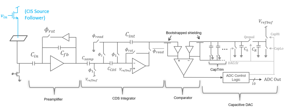
As shown in Fig 1, the input to SPROCKET2 is provided by a source-follower amplifier on the vertically-integrated Skipper-CCD-in-CMOS image sensor. The source follower is biased by a current source FET on SPROCKET2, and followed by a capacitive-feedback preamplifier and a discrete-time CDS integrator. These blocks make up the front-end; they work to amplify and sample the input signal, and integrate multiple samples on the capacitor in preparation for read-out.
The remainder of Fig 1 shows the in-pixel SAR ADC, which is substantially similar to the design presented in [9]. A capacitive DAC (CDAC) generates binary-weighted approximation voltages by charge-sharing between two capacitors, and , which are trimmed to match each other. The result is compared to the voltage stored across , and the output of the comparator determines the next bit in the successive approximation. Test results from SPROCKET1 showed that the trimming range of the CDAC capacitors was insufficient to compensate process mismatch in the worst case. SPROCKET2 improves upon the capacitor design by using a cross-coupled unit cell layout which provides better inherent matching.
Two reference voltages, and are distributed across the array. The references share an in-pixel buffer which switches output level based on the phase of operation.
III SPROCKET2 Test Pixel Initial Results
To characterize the performance of the SPROCKET2 ADC, a single pixel test structure was designed and fabricated. In this test structure, shown in Fig 2, the single pixel under test is abutted to three dummy pixels to form a square ”island” of custom circuitry surrounded by digital standard cells, which closely mimics the layout surroundings of the pixel when integrated into a full-chip array.
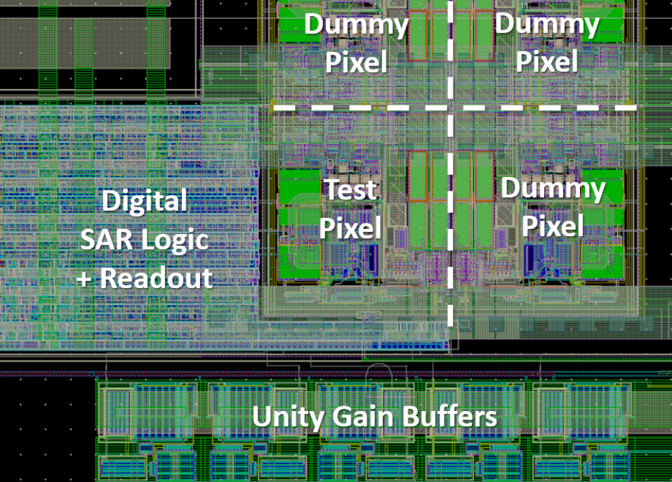
This test pixel was tested at a temperature of 100K using a closed-cycle cryocooler at Fermilab. The test pixel ADC was evaluated independently using the input (not shown), which allows for a voltage to be applied directly to the input of the ADC (the positive input of the comparator), bypassing the front end.
A code density histogram approach was used to characterize the non-linearity of the ADC for various trim capacitor settings. Optimal trim was found to be CapTrim=25, near the center of the trim range, which suggests that matching techniques were successful. Tests of the front-end show linear operation in all four gain regions, but due to nonidealities in the test setup, the design noise level has not yet been demonstrated. Work is ongoing, and more detailed results will be presented at the conference.
| FoM | Value | Comment |
|---|---|---|
| ADC Pixel Pitch | ||
| ADC Worst DNL | LSB | Measured, CapTrim=25 |
| ADC Worst INL | LSB | Measured, CapTrim=25 |
| Power | Simulated | |
| Resolution | Measured, Highest Gain Region | |
| Noise, Input RMS | Simulated, Highest Gain Region |
IV Conclusions and Future Work
The SPROCKET2 ADC provides a unique solution for reading out low-noise Skipper-CCD-in-CMOS detectors with unprecedented frame rates greater than 4 kfps. The operation of the architecture is validated by the presented measured results at cryogenic temperature. The next-generation SPROCKET chip (SPROCKET3) has already been taped out in December 2023. This chip integrates more than 20,000 ADC pixels using the architecture described above, along with on-chip biasing, pattern generation, and high-speed, low-power readout using silicon photonics. Ultimately SPROCKET3-FR (SPROCKET3 Full Reticle Version) will expand the SPROCKET read-out architecture to encompass a full 65nm reticle. We will present detailed results of both single pixel tests and array readout results.
References
- [1] J. Estrada, “Observatory of Skipper CCDs Unveiling Recoiling Atoms (OSCURA),” Available: https://astro.fnal.gov/science/dark-matter/oscura/, Accessed: 2021-05-01.
- [2] J. Janesick, K. Klaasen, and T. Elliott, “Ccd charge collection efficiency and the photon transfer technique,” in Solid-state imaging arrays, vol. 570. International Society for Optics and Photonics, 1985, pp. 7–19.
- [3] J. Janesick, Scientific charge-coupled devices. SPIE press, 2001, vol. 83.
- [4] G. Fernández Moroni, J. Estrada, G. Cancelo, S. E. Holland, E. E. Paolini, and H. T. Diehl, “Sub-electron readout noise in a skipper CCD fabricated on high resistivity silicon,” Experimental Astronomy, vol. 34, no. 1, pp. 43–64, 2012. [Online]. Available: https://doi.org/10.1007/s10686-012-9298-x
- [5] J. R. Janesick, T. S. Elliott, A. Dingiziam, R. A. Bredthauer, C. E. Chandler, J. A. Westphal, and J. E. Gunn, “New advancements in charge-coupled device technology: subelectron noise and 4096 x 4096 pixel CCDs,” in Charge-Coupled Devices and Solid State Optical Sensors, vol. 1242, 1990. [Online]. Available: https://doi.org/10.1117/12.19452
- [6] J. Tiffenberg et al., “Single-electron and single-photon sensitivity with a silicon skipper CCD,” Physical Review Letters, vol. 119, no. 13, p. 131802, 2017.
- [7] A. J. Lapi, M. Sofo-Haro, B. C. Parpillon, A. Birman, G. Fernandez-Moroni, L. Rota, F. A. Bessia, A. Gupta, C. C. Blanco, F. Chierchie et al., “Skipper-in-cmos: Non-destructive readout with sub-electron noise performance for pixel detectors,” arXiv preprint arXiv:2402.12516, 2024.
- [8] N. Wermes, “Pixel detectors … where do we stand?” Nuclear Instruments and Methods in Physics Research Section A: Accelerators, Spectrometers, Detectors and Associated Equipment, vol. 924, pp. 44–50, apr 2019. [Online]. Available: https://doi.org/10.1016\%2Fj.nima.2018.07.003
- [9] A. Quinn, M. B. Valentín, T. Zimmerman, D. Braga, S. O. Memik, and F. Fahim, “A cryogenic readout ic with 100 ksps in-pixel adc for skipper ccd-in-cmos sensors,” 2023 IEEE International Symposium on Circuits and Systems (ISCAS), pp. 1–5, 1900. [Online]. Available: https://api.semanticscholar.org/CorpusID:253374337
- [10] S. Miryala, D. Braga, D. C. Christian, G. W. Deptuch, P. Gui, J. R. Hoff, S. Holm, and X. Wang, “Cdp1—a data concentrator prototype for the deep underground neutrino experiment,” IEEE Transactions on Nuclear Science, vol. 66, no. 11, pp. 2338–2345, 2019.
- [11] D. Braga, S. Li, and F. Fahim, “Cryogenic electronics development for high-energy physics: An overview of design considerations, benefits, and unique challenges,” IEEE Solid-State Circuits Magazine, vol. 13, no. 2, pp. 36–45, 2021.