Non-Hermitian topology of transport in Chern insulators
Abstract
It has recently been shown that signatures of non-Hermitian topology can be realized in a conventional quantum Hall device connected to multiple current sources. These signatures manifest as robust current-voltage characteristics, dictated by the presence of a nontrivial, non-Hermitian topological invariant of the conductance matrix. Chiral edge states are believed to be responsible for this non-Hermitian response, similar to how they lead to a quantized Hall conductivity in the presence of a single current source. Here, we go beyond this paradigm, showing that multi-terminal conductance matrices can exhibit non-Hermitian topological phase transitions that cannot be traced back to the presence and directionality of a boundary-localized chiral mode. By performing quantum transport simulations in the quantum Hall regime of monolayer graphene, we find that when the chemical potential is swept across the zeroth Landau level, unavoidable device imperfections cause the appearance of an additional non-Hermitian phase of the conductance matrix. This highlights graphene as an ideal platform for the study of non-Hermitian topological phase transitions, and is a first step towards exploring how the geometry of quantum devices can be harnessed to produce robust, topologically-protected transport characteristics.
Introduction — A physical system can have a non-Hermitian topological description if it is coupled to an environment and the resulting gains and losses are customized to reach a topological phase [1, 2]. Such a topological phase offers robust characteristics, with potential applications such as light funnels [3], amplifiers [4], and exponentially precise sensors [5, 6]. The experimental realization of these phases usually relies on platforms where gain and loss can be precisely controlled in each individual building block. Examples include ultracold atoms [7], optical systems [8, 9], and meta-materials [10, 11, 3, 12, 13, 14, 15].
A recent study takes an alternative approach, which leverages the quantum transport properties of a well-known Hermitian topological phase – the quantum Hall phase in a GaAs/AlGaAs heterostructure [16]. In the presence of multiple current sources, the current-voltage characteristics of the quantum Hall phase show robust features that originate from the non-Hermitian topology of the conductance matrix, not of the Hamiltonian. The chiral edge modes ensure that charge propagates between neighboring contacts only in one direction, meaning that the multi-terminal conductance matrix becomes numerically equivalent to the Hamiltonian matrix of the Hatano-Nelson (HN) chain [17], a prototypical model of non-Hermitian topology. In effect, each terminal plays the role of a ‘site’ in the HN chain, while the edge modes propagating between adjacent contacts play the role of nearest-neighbor, one-way ‘hoppings.’
Away from the quantum Hall plateau regime, the bulk becomes conducting and diffusive transport occurs between any pair of contacts, such that the analogy between chiral edge modes and nonreciprocal nearest-neighbor hoppings breaks down. All elements of the non-Hermitian conductance matrix become sizeable, potentially leading to additional topological phases and phase transitions that are not the direct consequence of the chiral modes. Here, we demonstrate the emergence of an additional phase in the non-Hermitian, multi-terminal conductance matrix of Chern insulators. This extra phase is not caused by boundary-localized chiral modes, arising instead in the transition region between two quantum Hall plateaus with opposite Chern numbers. The topologically trivial phase is due to the inhomogeneities present in the conductance matrix, which occur in any experimental setup. Our work shows that, beyond the quantum Hall regime, the quality and geometry of multi-terminal devices can play an important role in generating robust current-voltage characteristics protected by non-Hermitian topology.
To illustrate this concept, we turn to graphene, one of the most accessible and highly-tunable platforms for realizing quantum Hall physics. Using a toy model, we first highlight the correspondence between chiral edge modes and the non-Hermitian topology of the conductance matrix. This correspondence remains valid even as the chemical potential is swept through the charge neutrality point and the edge modes change direction. Next, we introduce inhomogeneities into the multi-terminal conductance matrix, showing that they cause the emergence of an additional phase.
Transport in graphene and its connection to non-Hermitian topology — We use a toy model for graphene consisting of spinless fermions hopping on a honeycomb lattice. The Hamiltonian takes the form
| (1) |
where represents the on-site energy of an electron at the site index , represent its annihilation (creation) operator, denotes nearest neighbors, and is the hopping parameter. The unit cells are labeled by integers in the directions, respectively [see Fig. 1(a)].
We introduce a perpendicular magnetic field by changing the vertical hoppings in Fig. 1(a) from to , where is the flux per hexagon, in units of the flux quantum. This gaps out the Dirac cones and results in the formation of Landau levels, symmetrically distributed around the charge neutrality point, [18] (see the supplemental material (SM) for details [19]). Since the model is spinless, sweeping the chemical potential from to reverses the edge mode propagation direction from counter-clockwise to clockwise, leading to a direct transition between phases with Chern numbers and .
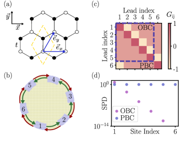
Using the Kwant package [20], we attach equally-spaced ideal leads to the boundary of a finite-sized, disk-shaped system, as shown in Fig. 1(b) for . Numerical details are described in the SM [19]. This models an experimental setup in which contacts are connected to a graphene sample. In the linear regime, the currents injected into each of the contacts, , are related to the potentials on each of the contacts, , as , where is the conductance matrix. At zero-temperature and in the zero bias voltage limit, the elements of take the form
| (2) |
Here, is the electric charge, is Planck’s constant, denotes the Kronecker delta, is the number of propagating modes in lead , and denotes the trace. The matrix is a block of the full, multi-terminal scattering matrix, containing the probability amplitudes for a particle to be transmitted from any incoming mode of lead to any outgoing mode of lead .
For the six-terminal system shown in Fig. 1(b), setting and , such that the system is deep in the quantum Hall phase with Chern number , leads to the conductance matrix shown in Fig. 1(c). This matrix is identical to the non-Hermitian Hamiltonian matrix of the Hatano-Nelson tight-binding model [17], a chain of orbitals connected by nonreciprocal nearest-neighbor hoppings. Thus, each of the diagonal elements can be thought of as being analogous to the onsite energy of a site in the fictitious chain. The off-diagonal elements are analogous to hopping integrals connecting the different fictitious sites. In this case, each of the sites has an onsite energy equal to , one-way hoppings equal to connect the and sites, and since , the chain has periodic boundary conditions (PBC). Realizing an analogue of the Hatano-Nelson model with open boundary conditions (OBC) can be done by grounding the contact (setting the potential ). In this case the currents and voltages corresponding to the first five terminals would be related by the conductance sub-matrix, , shown by the dashed box in Fig. 1(c).
The nontrivial topology of the Hatano-Nelson Hamiltonian matrix, and thus of the multi-terminal conductance matrix, results in robust current-voltage characteristics. A transport regime in which the current vector is proportional to the voltage vector can only be reached provided that these vectors are eigenvectors of the conductance matrix. In the OBC case (grounded contact), all eigenvectors are exponentially localized to one end of the fictitious Hatano-Nelson chain, a non-Hermitian topological phenomenon referred to as the non-Hermitian skin effect [21, 22]. This can be seen from the probability density summed over all right eigenvectors of the conductance matrix, . Thus, when the currents and voltages on terminals to follow the exponentially decaying pattern shown in Fig. 1(d).
In contrast, for the PBC setup, when the six currents and voltages do not show an exponential profile. Both of these proportionality regimes can be reached in a robust and predictable way by means of iterative transport measurements, as shown experimentally in Ref. [16].
Inhomogeneity and topological phase transitions — We are interested in studying the topology of the conductance matrix away from the quantum Hall plateau regime, when bulk transport is significant and all elements of are nonzero. To this end, we follow Refs. [23, 16], and focus only on the OBC setup in the following. The contact is grounded at all times and only the sub-block of the conductance matrix, , is considered. We use a topological invariant, , that can be determined directly from this conductance matrix, and which predicts the existence of a non-Hermitian skin effect. To compute it, we first subtract the average of the diagonal elements from the conductance matrix, , where and is the identity matrix. Writing the polar decomposition of this matrix, , where is unitary and is a positive-definite matrix, yields
| (3) |
where encodes the lead index, and is the trace per unit volume evaluated over the middle indices, far from the ends (see SM for details [19]).
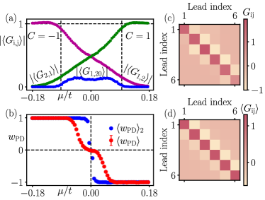
As expected, we confirm that correctly predicts the appearance of a non-Hermitian skin effect in the conductance matrix of Fig. 1(d). Deep in the quantum Hall plateau regime, where the boundary-localized chiral modes produce one-way nearest-neighbor hoppings of the fictitious Hatano-Nelson chain, the invariant in Eq. (3) is locked to the Chern number. We have verified that sweeping the chemical potential across the charge neutrality point leads to a direct transition in the Chern number from to , and simultaneously to a direct transition of , from to . Correspondingly, there is a change of direction in the non-Hermitian skin effect: all eigenvectors of the conductance matrix are all localized either on the left or the right side of the chain, depending on the sign of .
In any experiment, we expect that the conductance matrix will be inhomogeneous due to multiple factors. These include the varying quality of different contacts, unequal distances between them, as well as disorder and defects in the sample. For simplicity, we obtain inhomogeneous conductance matrices by randomly changing the potential on each site of the honeycomb lattice, , where is chosen from a uniform distribution .
The average non-Hermitian topological invariant of the conductance matrix can be expressed as:
| (4) |
for independent realizations of the random onsite potential, each producing a different conductance matrix . Figure 2 shows that for the conductance matrix exhibits a direct transition from to as the chemical potential is swept across the charge neutrality point, as mentioned above. Turning on inhomogeneities, however, leads to the appearance of a trivial phase of the conductance matrix, , for which the current-voltage characteristics do not show the exponential profile of the non-Hermitian skin effect (see SM for details [19]). We observe that increasing leads to an enlargement of this phase, which appears for a wider range of chemical potential .
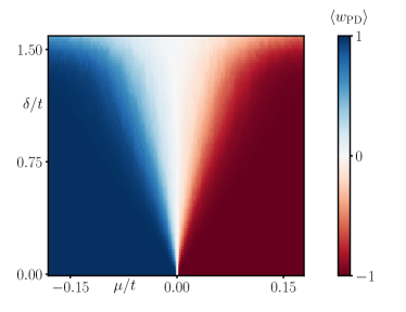
The intervening trivial non-Hermitian phase of the conductance matrix appears in a region where the bulk of the graphene is conducting, due to the fact that random potential fluctuations broaden the zeroth Landau level. However, it is not caused by the presence of conducting bulk modes. To show this, we consider a different averaging scheme, where we first average the conductance matrix over the random realizations of onsite disorder, and only afterwards compute the topological invariant:
| (5) |
This procedure leads to a conductance matrix with uniform entries on each diagonal, where the broadening of the zeroth Landau level is still present, but does not produce an extra non-Hermitian phase in the conductance matrix (see Fig. 3).
The true reason for emergence of the extra phase between phases is due to inhomogeneities in the conductance matrix and is a natural consequence of the current conservation rules. Since the sum of all elements of over any column must vanish due to Kirchhoff’s laws, , random conductance fluctuations between different pairs of leads necessarily lead to random changes on the conductance matrix diagonal. On the level of the fictitious, 1D Hatano-Nelson chain simulated by , this corresponds to the presence of onsite disorder, which is known to lead to an extra phase (see Ref. [23] and SM [19]).
Conclusion — We have theoretically investigated the non-Hermitian topological behavior associated with multiple-current-source transport in Chern insulators, using the quantum Hall phases of a honeycomb graphene model as an example. Our simulations demonstrated the presence and robustness of non-Hermitian phases in the conductance matrix of this system, which can easily be tuned through chemical potential variations. This variation can be achieved in practice via gate voltage adjustments, making graphene a promising platform to realize current-voltage relations protected non-Hermitian topology.
Interestingly, we found that inhomogeneities in the conductance matrix, which can arise, e.g. due to varying contact quality or inter-contact distance lead to the emergence of an additional, trivial non-Hermitian phase in the system’s conductance matrix. This implies that away from the quantum Hall plateau regime, the quality and geometry of quantum devices may play a decisive role in producing transport properties associated with non-Hermitian topology. Further, while we have focused on a graphene toy model for simplicity, we expect this behavior to be generic to a larger class of Chern insulators, including those realized in magnetically doped topological insulators [24].
Data availability— The data and code used to generate the figures are available at [25].
Acknowledgments — We thank Ulrike Nitzsche for her technical assistance. We acknowledge funding by the Deutsche Forschungsgemeinschaft (DFG, German Research Foundation) through SFB 1170, Project-ID 258499086, and through the Würzburg-Dresden Cluster of Excellence on Complexity and Topology in Quantum Matter – ct.qmat (EXC2147, Project-ID 390858490). V.K. was funded by the European Union.
References
- Ashida et al. [2020] Y. Ashida, Z. Gong, and M. Ueda, Non-Hermitian physics, Adv. Phys. 69, 249 (2020).
- Bergholtz et al. [2021] E. J. Bergholtz, J. C. Budich, and F. K. Kunst, Exceptional topology of non-Hermitian systems, Rev. Mod. Phys. 93, 015005 (2021).
- Weidemann et al. [2020] S. Weidemann, M. Kremer, T. Helbig, T. Hofmann, A. Stegmaier, M. Greiter, R. Thomale, and A. Szameit, Topological funneling of light, Science 368, 311 (2020).
- Wang et al. [2022] Q. Wang, C. Zhu, Y. Wang, B. Zhang, and Y. Chong, Amplification of quantum signals by the non-Hermitian skin effect, Phys. Rev. B. 106, 024301 (2022).
- Budich and Bergholtz [2020] J. C. Budich and E. J. Bergholtz, Non-Hermitian topological sensors, Phys. Rev. Lett. 125, 180403 (2020).
- Könye et al. [2023] V. Könye, K. Ochkan, A. Chyzhykova, J. C. Budich, J. van den Brink, I. C. Fulga, and J. Dufouleur, Non-Hermitian topological ohmmeter (2023), arXiv:2308.11367 .
- Liang et al. [2022] Q. Liang, D. Xie, Z. Dong, H. Li, H. Li, B. Gadway, W. Yi, and B. Yan, Dynamic signatures of non-Hermitian skin effect and topology in ultracold atoms, Phys. Rev. Lett. 129, 070401 (2022).
- Xiao et al. [2020] L. Xiao, T. Deng, K. Wang, G. Zhu, Z. Wang, W. Yi, and P. Xue, Non-Hermitian bulk–boundary correspondence in quantum dynamics, Nat. Phys. 16, 761 (2020).
- Wang et al. [2021] H. Wang, X. Zhang, J. Hua, D. Lei, M. Lu, and Y. Chen, Topological physics of non-Hermitian optics and photonics: a review, J. Opt. 23, 123001 (2021).
- Helbig et al. [2020] T. Helbig, T. Hofmann, S. Imhof, M. Abdelghany, T. Kiessling, L. W. Molenkamp, C. H. Lee, A. Szameit, M. Greiter, and R. Thomale, Generalized bulk–boundary correspondence in non-Hermitian topolectrical circuits, Nat. Phys. 16, 747 (2020).
- Liu et al. [2021] S. Liu, R. Shao, S. Ma, L. Zhang, O. You, H. Wu, Y. J. Xiang, T. J. Cui, and S. Zhang, Non-Hermitian Skin Effect in a Non-Hermitian Electrical Circuit, Research 2021, 1 (2021).
- Brandenbourger et al. [2019] M. Brandenbourger, X. Locsin, E. Lerner, and C. Coulais, Non-reciprocal robotic metamaterials, Nat. Commun. 10, 1 (2019).
- Ghatak et al. [2020] A. Ghatak, M. Brandenbourger, J. Van Wezel, and C. Coulais, Observation of non-Hermitian topology and its bulk-edge correspondence in an active mechanical metamaterial, PNAS 117, 29561 (2020).
- Zhang et al. [2021a] X. Zhang, Y. Tian, J. H. Jiang, M. H. Lu, and Y. F. Chen, Observation of higher-order non-Hermitian skin effect, Nat. Commun. 12, 1 (2021a).
- Zhang et al. [2021b] L. Zhang, Y. Yang, Y. Ge, Y. J. Guan, Q. Chen, Q. Yan, F. Chen, R. Xi, Y. Li, D. Jia, S. Q. Yuan, H. X. Sun, H. Chen, and B. Zhang, Acoustic non-Hermitian skin effect from twisted winding topology, Nat. Commun. 12, 1 (2021b).
- Ochkan et al. [2024] K. Ochkan, R. Chaturvedi, V. Könye, L. Veyrat, R. Giraud, D. Mailly, A. Cavanna, U. Gennser, E. M. Hankiewicz, B. Büchner, J. van den Brink, J. Dufouleur, and I. C. Fulga, Non-Hermitian topology in a multi-terminal quantum Hall device, Nat. Phys. 20, 395 (2024).
- Hatano and Nelson [1996] N. Hatano and D. R. Nelson, Localization transitions in non-Hermitian quantum mechanics, Phys. Rev. Lett. 77, 570 (1996).
- Novoselov et al. [2005] K. S. Novoselov, A. K. Geim, S. V. Morozov, D. Jiang, M. I. Katsnelson, I. V. Grigorieva, S. V. Dubonos, and A. A. Firsov, Two-dimensional gas of massless Dirac fermions in graphene, Nature 438, 197 (2005).
- [19] See Supplementary Material at [URL] for details on our numerical simulations, a scaling analysis of the additional non-Hermitian phase, and a study of the difference in non-Hermitian skin effect between individual and averaged conductance matrices.
- Groth et al. [2014] C. W. Groth, M. Wimmer, A. R. Akhmerov, and X. Waintal, Kwant: a software package for quantum transport, New J. Phys. 16, 063065 (2014).
- Martinez Alvarez et al. [2018] V. M. Martinez Alvarez, J. E. Barrios Vargas, and L. E. F. Foa Torres, Non-Hermitian robust edge states in one dimension: Anomalous localization and eigenspace condensation at exceptional points, Phys. Rev. B 97, 121401 (2018).
- Yao and Wang [2018] S. Yao and Z. Wang, Edge states and topological invariants of non-Hermitian systems, Phys. Rev. Lett. 121, 086803 (2018).
- Claes and Hughes [2021] J. Claes and T. L. Hughes, Skin effect and winding number in disordered non-Hermitian systems, Phys. Rev. B 103, L140201 (2021).
- Chang et al. [2013] C.-Z. Chang, J. Zhang, X. Feng, J. Shen, Z. Zhang, M. Guo, K. Li, Y. Ou, P. Wei, L.-L. Wang, Z.-Q. Ji, Y. Feng, S. Ji, X. Chen, J. Jia, X. Dai, Z. Fang, S.-C. Zhang, K. He, Y. Wang, L. Lu, X.-C. Ma, and Q.-K. Xue, Experimental observation of the quantum anomalous Hall effect in a magnetic topological insulator, Science 340, 167 (2013).
- Chaturvedi et al. [2024] R. Chaturvedi, V. Könye, E. M. Hankiewicz, J. van den Brink, and I. C. Fulga, Non-Hermitian topology of transport in Chern insulators, Zenodo https://doi.org/10.5281/zenodo.12166403 (2024).