s.souma@arpes.phys.tohoku.ac.jp
t-sato@arpes.phys.tohoku.ac.jp††thanks: Corresponding authors:
s.souma@arpes.phys.tohoku.ac.jp
t-sato@arpes.phys.tohoku.ac.jp
Universal Role of Combined Symmetry for the Protection of the Dirac Cone in Antiferromagnetic Topological Insulators
Abstract
Antiferromagnetic topological insulators (AF TIs) are predicted to exhibit exotic physical properties such as gigantic optical and topological magnetoelectric responses. While a key to achieving such phenomena relies on how to break the symmetry protecting the Dirac-cone surface state (SS) and acquire the mass of Dirac fermions, the mechanism has yet to be clarified. To address this issue, we carried out micro-focused angle-resolved photoemission spectroscopy for GdBi hosting the type-II AF order, and uncovered the stripe-type 21 reconstruction of the Fermi surface associated with the AF band folding. Intriguingly, in contrast to NdBi with the type-I AF order displaying the surface-selective Dirac-fermion mass, GdBi shows massless behavior irrespective of AF domains due to the robust topological protection. These results strongly suggest a crucial role of the TD (time-reversal and translational) symmetry to create the Dirac-fermion mass in AF TIs.
I INTRODUCTION
TIs are characterized by the boundary state showing linearly dispersive energy bands with a band crossing at the Dirac point [1, 2]. Symmetries that guarantee such a Dirac-band crossing play a key role in realizing various topological quantum phenomena [3, 4, 5]. For example, in nonmagnetic TIs, the introduction of ferromagnetic (FM) order breaks the time-reversal symmetry (TRS; ) and lifts the band degeneracy at the Dirac point, leading to quantum anomalous Hall effect [6, 7, 8]. Unlike TRS-broken ferromagnets, many antiferromagnets with a periodic arrangement of magnetic moments have a symmetry analogous to the TRS [9]. This is called S symmetry which is the combination of time-reversal operation and translational operation TD (S = TD) where the D vector connects antiparallel spins so that the S symmetry preserves the structure of antiferromagnets. The AF TIs with the S symmetry at the surface are characterized by the Z2 topological invariant and host the Dirac-cone SS as in the case of time-reversal-invariant TIs [9, 10]. Intriguingly, when the S symmetry is broken at the surface with a particular mirror index, an energy gap (Dirac gap) opens at the Dirac point and as a result the Dirac fermions become massive. This S-symmetry-broken surface leads to the emergence of chiral edge modes [9, 11, 12, 13] and was theoretically predicted to show unique phenomena such as quantized magnetoelectric effect [4, 9, 14, 15, 16], giant optical responses [14, 17, 18, 19], and axion electrodynamics [20, 21]. AF TIs also provide a unique opportunity to manipulate the topological properties via controlling the magnetic domains and Néel vectors [22, 23, 24].
Despite these theoretical predictions, it is still experimentally unclear whether or not the S symmetry plays an essential role in characterizing the Dirac-cone SS in AF TIs. This is highlighted in the case of MnBi2Te4 (MBT) which was proposed as the first material platform of AF TIs. MBT is a van-der Waals AF insulator containing a septuple layer in a unit cell with a ferromagnetic Mn layer placed at the center layer wherein adjacent Mn layers are antiferromagnetically coupled [25]. At the surface parallel to the septuple layer obtained by the cleaving of the crystal, the S symmetry is broken, resulting in the opening of a Dirac gap of 70 meV [25]. The predicted Dirac gap was indirectly supported by the transport measurements with thin flakes of MBT [26, 27]. On the other hand, it is hard to access the S-symmetry-preserved surface because the cleaving plane is limited to that parallel to the layer. This hinders the understanding of the relationship between the S symmetry and the Dirac gap.
Recently, rare-earth monopnictide NdBi was proposed to be an AF TI characterized by the topological SS protected by the S symmetry [28]. NdBi has a cubic rock-salt crystal structure and shows an inverted bulk-band structure that supports the strong TI nature in the paramagnetic (PM) phase. Below the Néel temperature (), the type-I AF order with the propagation vectors of [100], [010], and [001] directions (equivalent to in a cubic lattice) is stabilized, creating three different types of AF domains on the cleaved (001) surface. Angle-resolved photoemission spectroscopy (ARPES) study has identified the AF-domain-dependent Dirac-fermion mass, supporting the protection of Dirac cones by the S symmetry [28]. On the other hand, an unusual SS, distinct from the Dirac cone, has been observed in NdBi and other type-I AF monopnictides, requiring deeper understanding of the role of symmetries in magnetic topological materials [29, 30, 31]. A key to resolve such a complex situation on the interplay between the symmetry and the surface band structure lies in the investigation of topological SS for materials with different AF structures. Here, we deliberately chose GdBi as a target material of ARPES investigation, because it exhibits the type-II AF order [Fig. 1(a)] with the propagation vector along the direction, distinct from the type-I order of NdBi with the direction.
II EXPERIMENTS
GdBi single crystals were grown by the Bridgman method in a high-vacuum furnace equipped with a tungsten heater. High-purity starting materials of Gd (3N) and Bi (6N) with a ratio of 1:1 were sealed in a tungsten crucible using an electron-beam welder. The crucible was heated above the melting point of sealed materials (2,100 ) and then slowly pulled down from the heater. After that, the crucible was slowly cooled down to room temperature. Obtained crystals were characterized by x-ray diffraction and magnetization measurements.
Vacuum-ultraviolet (VUV)-ARPES measurements were performed at BL-28A in Photon Factory (PF) with circularly polarized 60–200 eV photons using a micro beam spot of 12 10 [32]. Soft-x-ray (SX) ARPES measurements were performed at BL-2A (Musashi) in PF with linearly polarized light (horizontal polarization) of 536 eV. The energy resolution for VUV and SX-ARPES measurements was set to be 10–30 meV and 150 meV, respectively. Samples were cleaved in situ in an ultrahigh vacuum of Torr along the (001) crystal plane. The Fermi level (EF) of the samples was referenced to that of a gold film evaporated onto the sample holder.
First-principles band-structure calculations were carried out by using the projector augmented wave method implemented in the Vienna Abinitio Simulation Package (VASP) code [33]. To calculate the band structure in the PM phase, the modified Becke–Johnson (mBJ) potential [34], which is known to properly reproduce the band gap in rare-earth monopnictides [35], was used for the exchange-correlation functional. The total energy was calculated self-consistently with the tetrahedron sampling of k-point mesh taking into account spin-orbit coupling. The SS was obtained with the surface Green’s function method implemented in WannierTools code [36] after the maximally localized Wannier functions for Bi-s, Bi-p, and Gd-d orbital states were obtained by using Wannier90 code [37].
III RESULTS AND DISCUSSION
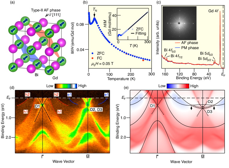
First, we present a characterization of a GdBi single crystal grown by the Bridgman method. Temperature dependence of magnetic susceptibility in Fig. 1(b) signifies a peak at 27.5 K associated with the AF transition, consistent with the previous report [38]. The shows a linear temperature dependence above of 27.5 K (inset), suggesting that contributions from core diamagnetism, Pauli paramagnetism, and van Vleck paramagnetism are small. As shown in Fig. 1(c), the core-level photoemission spectrum in a wide binding energy () region is composed only of the Bi- and Gd-derived peaks, and the Laue diffraction pattern shows sharp spots with four-fold symmetry of the (001) cleaving plane. These suggest the high-quality nature of our bulk crystal.
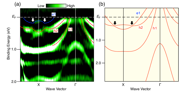
To clarify the existence of topological Dirac-cone SS in the PM phase, we carried out surface-sensitive ARPES measurements with VUV photons in a wide valence-band region along the cut of surface Brillouin zone (BZ), as shown in Fig. 1(d). The existence of topological SS in the PM phase is a necessary condition for GdBi to become an AF TI below . Due to the spectral broadening along the wave vector perpendicular to the surface associated with the short escape depth of photoelectrons, the ARPES signal for the bulk states reflects the electronic structure integrated over a large area [28, 39]. In the experiment, one can recognize two hole bands centered at the point, h1 and h2, showing stronger and weaker intensities, respectively, both of which are ascribed to the bulk Bi 6p bands at the plane. We also find a shallow and weak electron band e1 which is attributed to the Gd 5d band at . DFT calculations along the X cut of bulk BZ (corresponding to the cut in the surface BZ) shown by black curves in Fig. 1(e) reproduce well the experimental h1, h2 and e1 bands. Importantly, according to the DFT calculations, the h2 and e1 bands show an inverted band structure at the point producing a small spin-orbit gap at their intersection slightly away from the point (black arrows; see Appendix A for details). In fact, our parity analysis on the calculated band structure at eight time-reversal-invariant momenta (TRIMs) shows topological invariants of , supporting that GdBi is a strong TI with a negative band gap in the PM phase, as in other RBi compounds such as NdBi [28]. Associated with the bulk-band inversion at the bulk X point, single (called D1) and double (called D2 and D3) Dirac-cone SSs appear at the and points, respectively, corresponding to the number of band inversions projected onto the surface BZ. Such Dirac-cone SSs are identified in both the experiment [Fig. 1(d)] and the theoretically-calculated surface spectral weight obtained with the Green’s function method [Fig. 1(e)]. It is noted that the energy separation between the Dirac points of the D2 and D3 SSs at the point is very close to each other, and the energy dispersion of the D3 SS is less clear due to the stronger interaction with the bulk states.
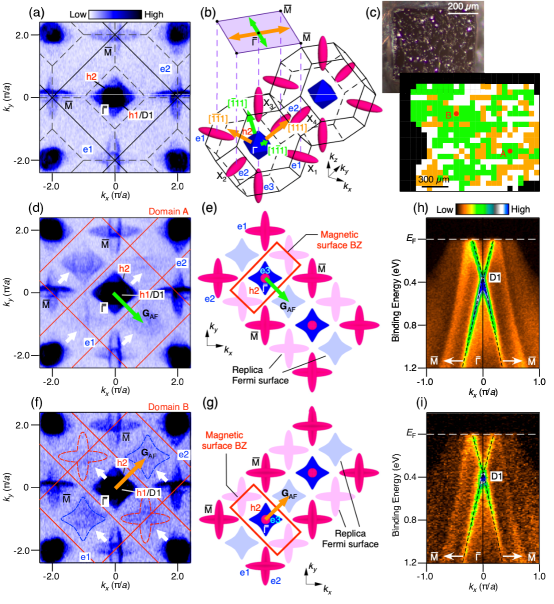
To examine the influence of type-II AF order on the fermiology, we carried out Fermi-surface mapping across . As shown in Fig. 2(a), the ARPES intensity in the PM phase is dominated by the warped square-like outer hole pocket at the point (h2) and the cross-shaped electron pockets (e1 and e2) at the point, consistent with the semimetallic bulk-band structure shown in Fig. 2(b) under the influence of strong broadening (note that the h1 and D1 pockets are inside the h2 pocket and not clearly visible). We have examined homogeneity of the observed electronic structure by scanning the whole area of the cleaved surface with the micro beam spot. As a result, we found that the intensity pattern is homogeneously distributed over the entire surface in the PM phase, whereas the intensity in the AF phase exhibits two different types of patterns depending on the position of the surface. We categorize these as domains A and B, respectively, and their distribution is visualized by green and orange colors in Fig. 2(c). As shown in Fig. 2(d), the intensity distribution for domain A is apparently different from that of the PM phase [Fig. 2(a)]. Besides the Fermi surface seen in the PM phase, we found a replica of the -centered square pocket with a reduced intensity midway between the first and second points; specifically, at and (-1.0, 1.0) in a unit of . This results in a 1D array of square pockets running along the lower-right/upper-left direction [see also schematics in Fig. 2(e)]. Such replicas are also observed for the centered cross-shaped pockets at and (-1.0, -1.0), resulting in the stripe-type reconstruction of the Fermi surface. In domain B [Figs. 2(f) and 2(g)], all these replica pockets are resolved, but the direction of 1D array is different; it runs along the lower-left/upper-right direction, rotated by from that of domain A. All these features are well explained in terms of the AF-induced band folding with two types of surface-projected AF ordering vectors depicted by (green and orange arrows) in Figs. 2(d)–2(g). When we take into account the cubic symmetry of bulk crystal and the type-II AF order, there exist four types of AF domains in the bulk characterized by four AF-ordering vectors, , ,, and [orange and green arrows in the bulk BZ in Fig. 2(b)]. When these vectors are projected onto the (001) surface [surface BZ with purple shade in Fig. 2(b)], two of them, e.g. and exhibit the same band folding, leading to the distinction of two types of AF domains by ARPES. Despite such strong domain-dependent Fermi-surface modulation, we found that the Dirac-cone band (D1) at the point seen in the PM phase remains unchanged even in the AF phase. As shown in Figs. 2(h) and 2(i), one can commonly recognize the gapless X-shaped D1 band for both domains A and B.
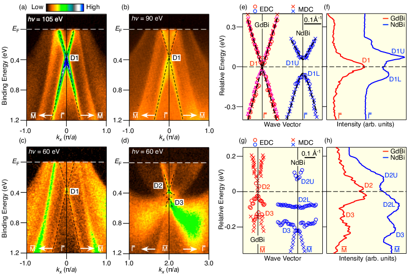
We have confirmed that the D1 band in the AF phase is indeed of surface origin by observing that the band dispersion is robust against variation despite a change in the intensity relative to the bulk hole bands h1 and h2 [Figs. 3(a)–3(h)]. We also found that the D2 band shows a negligible change across and preserves the gapless character below [Fig. 3(d)], as in the case of the D1 band [note that it was difficult to trace the whole dispersion of the D3 band in the experiment likely due to the stronger interaction with the bulk states, as inferred from the DFT calculation in Fig. 1(e)]. Such AF-transition-insensitive nature of the D1 band is distinctly different from the behavior of isostructural NdBi [28] with the type-I AF order showing an energy gap of in the AF phase on the top surface [see also Fig. 4(c)], as highlighted by a side-by-side comparison of the experimental D1-band dispersion between GdBi and NdBi in Fig. 3(e). This is also evident from the EDC at the point [Fig. 3(f)], which shows a single peak in GdBi while a two-peaked structure is seen in NdBi. Intriguingly, a similar trend was also identified for the D2 band; the D2 band in NdBi shows an energy gap [blue circles in Fig. 3(g)] accompanied by the double-peaked feature in the EDC [blue curve in Fig. 3(h)], while in GdBi such an energy gap is not clearly seen [red markers in Fig. 3(g)] and the EDC shows a single peak [red curve in Fig. 3(h)].
It is emphasized here that, in FM TIs, the out-of-plane component of magnetic moment at the surface is essential to create a finite Dirac-fermion mass associated with the TRS breaking. On the other hand, GdBi with the type-II AF structure always shows a massless Dirac cone at the surface with a finite out-of-plane magnetic component [Fig. 1(a)]. This strongly suggests that the TRS alone cannot account for the Dirac-cone protection in GdBi, requiring consideration of other symmetries unique to the AF structure.
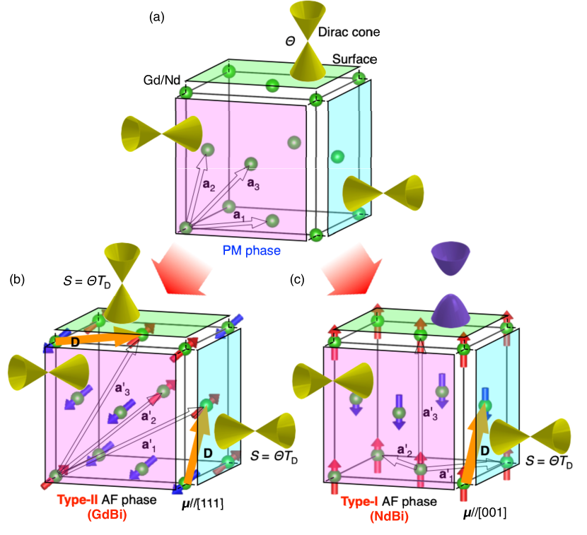
Now we discuss a critical difference in the nature of the surface Dirac-fermion mass between GdBi and NdBi. In the PM phase, both compounds commonly show bulk-band inversion and gapless Dirac-cone SS associated with the topology on the (001) cleaved surface [Fig. 4(a)], and their topological properties are essentially the same with each other. On the other hand, in the AF phase, GdBi and NdBi show different (type-II and type-I, respectively) AF order [Figs. 4(b) and 4(c)]. In NdBi, the type-I AF order leads to three types of AF domains on the (001) surface with the magnetic propagation vectors running along the [100], [010], and [001] axes, respectively. In a rock-salt crystal, equivalently, one can consider the single AF domain with the fixed ordering vector and three cleaving planes (100), (010), and (001), as shown in Fig. 4(c). Since the (100) and (010) surfaces (side surfaces) have the D vector (the translation that inverts the spin direction) lying on the surface, the combined symmetry S is preserved, and the Dirac cone keeps the massless character. On the other hand, the S symmetry is broken on the (001) surface (top surface) and the Dirac cone becomes massive because the D vector cannot be defined parallel to the surface. This leads to the weak-TI-like behavior on the Dirac-cone SS in NdBi. In GdBi, there exist two types of AF domains in the (001) surface with propagation vectors of [110] and (see also Fig. 2). In this case, one can define the D vectors parallel to the surface for both the top and side surfaces [Fig. 4(b)], leading to the emergence of gapless Dirac cones and strong-TI-like characteristics. This consideration led us to conclude that the S symmetry is crucial for determining the massive vs. massless character of Dirac fermions in AF TIs independently of the AF structures. This conclusion is reasonable because only the S symmetry is a common symmetry between surface and bulk among various crystal symmetries (e.g. I, , ) in the AF phase of GdBi (magnetic space group; , No. 167.108 [40, 41]).
The present results confirm the theoretically proposed condition (: a vector normal to the surface) to keep the gapless Dirac-cone SS in AF TIs with the S symmetry [9, 10]. Here, the vector hosting the gapless Dirac-cone SS is generally written as,
| (1) |
where [shown by open black arrows in Figs. 4(a)–4(c)] and are the unit vector in the AF phase and an arbitrary integer, respectively, and is 0 or 1 (at least one of ’s must be 1) [10]. The gapless surfaces of NdBi and GdBi in the AF phase satisfy the above condition, because the shortest D vector for NdBi can be written with the set of and , whereas in GdBi the and are (-1, 0, 0) and (1, 1, 1), respectively [orange arrows in Figs. 4(b) and 4(c)]. Thus, in AF TIs, the deliberate choice of a surface with a suitable mirror index can lead to the S-symmetry-broken massive Dirac-cone SS which is a prerequisite to realizing -originated optical and electromagnetic responses [10, 14]. In this respect, the AF TIs with S symmetry are advantageous to realize the exotic quantum phenomena, compared to the FM case which often requires the complex hetero-junction of TI and ferromagnet. Such surface engineering utilizing the S-symmetry-characterized Dirac-cone SS is the next step to realizing exotic phenomena unique to AF TIs.
IV CONCLUSION
We have performed AF-domain-selective micro-ARPES measurements on type-II antiferromagnet GdBi, and uncovered (i) stripe-type reconstruction of Fermi surface associated with the AF band folding and (ii) robust gapless Dirac-cone SS in the AF phase in contrast to surface-selective Dirac gap in isostructural type-I antiferromagnet NdBi. Our result strongly suggests the universal role of S symmetry for the protection of the Dirac cone in AF TIs, and paves a pathway toward realizing exotic quantum phenomena in AF TIs.
Acknowledgements.
We thank T. Kato, T. Osumi, and Y. Kondo for their assistance in the ARPES experiments. This work was supported by JST-CREST (No. JPMJCR18T1), Grant-in-Aid for Scientific Research (JSPS KAKENHI Grant Numbers JP21H04435 and JP24K00564), Grant-in-Aid for JSPS Research Fellow (No: JP23KJ0210), KEK-PF (Proposal number: 2021S2-001, 2024S2-001, and 2022G652), and UVSOR. The work in Cologne was funded by the Deutsche Forschungsgemeinschaft (DFG, German Research Foundation) - Project number 277146847 - CRC 1238 (Subproject A04). A.H. thanks GP-Spin and JSPS, and D.T. thanks JSPS and Tohoku University Division for Interdisciplinary Advanced Research and Education.Appendix A BULK BAND INVERSION IN GdBi
Bulk-sensitive SX ARPES is advantageous in visualizing the bulk band dispersion of GdBi. Figure 5 shows the plot of the second derivative intensity of the ARPES spectrum along the cut of bulk BZ measured with . The plot signifies a weak Gd 5d electron band e1 (dashed blue curve) which crosses midway between the and X points, together with the inner (h1) and outer (h2) Bi-6p hole bands around the point. The e1 and h2 bands appear to show a hybridization gap at the intersections (white arrows), suggestive of the inverted band structure as in the case of other RBi compounds [39, 35, 28]. As shown in Fig. 5(b), ARPES-derived band dispersions are well reproduced by our band-structure calculations including the spin-orbit coupling which signifies the bulk band inversion with a small spin-orbit gap (see black arrows). These results, together with the observation of Dirac-cone SS in the PM phase [Fig. 1(d)], support the TI nature of GdBi in the PM phase.
References
- Fu et al. [2007] L. Fu, C. L. Kane, and E. J. Mele, Topological Insulators in Three Dimensions, Phys. Rev. Lett. 98, 106803 (2007).
- Hsieh et al. [2008] D. Hsieh, D. Qian, L. Wray, Y. Xia, Y. S. Hor, R. J. Cava, and M. Z. Hasan, A Topological Dirac Insulator in a Quantum Spin Hall Phase, Nature (London) 452, 970 (2008).
- Qi et al. [2008] X.-L. Qi, T. L. Hughes, and S.-C. Zhang, Topological Field Theory of Time-Reversal Invariant Insulators, Phys. Rev. B 78, 195424 (2008).
- Turner et al. [2012] A. M. Turner, Y. Zhang, R. S. K. Mong, and A. Vishwanath, Quantized Response and Topology of Magnetic Insulators with Inversion Symmetry, Phys. Rev. B 85, 165120 (2012).
- Fu [2011] L. Fu, Topological Crystalline Insulators, Phys. Rev. Lett. 106, 106802 (2011).
- Yu et al. [2010] R. Yu, W. Zhang, H.-J. Zhang, S.-C. Zhang, X. Dai, and Z. Fang, Quantized Anomalous Hall Effect in Magnetic Topological Insulators, Science 329, 61 (2010).
- Chang et al. [2013] C.-Z. Chang, J. Zhang, X. Feng, J. Shen, Z. Zhang, M. Guo, K. Li, Y. Ou, P. Wei, L.-L. Wang, Z.-Q. Ji, Y. Feng, S. Ji, X. Chen, J. Jia, X. Dai, Z. Fang, S.-C. Zhang, K. He, Y. Wang, L. Lu, X.-C. Ma, and Q.-K. Xue, Experimental Observation of the Quantum Anomalous Hall Effect in a Magnetic Topological Insulator, Science 340, 167 (2013).
- Checkelsky et al. [2014] J. G. Checkelsky, R. Yoshimi, A. Tsukazaki, K. S. Takahashi, Y. Kozuka, J. Falson, M. Kawasaki, and Y. Tokura, Trajectory of the Anomalous Hall Effect towards the Quantized State in a Ferromagnetic Topological Insulator, Nat. Phys. 10, 731 (2014).
- Mong et al. [2010] R. S. K. Mong, A. M. Essin, and J. E. Moore, Antiferromagnetic Topological Insulators, Phys. Rev. B 81, 245209 (2010).
- Fang et al. [2013] C. Fang, M. J. Gilbert, and B. A. Bernevig, Topological Insulators with Commensurate Antiferromagnetism, Phys. Rev. B 88, 085406 (2013).
- Essin et al. [2009] A. M. Essin, J. E. Moore, and D. Vanderbilt, Magnetoelectric Polarizability and Axion Electrodynamics in Crystalline Insulators, Phys. Rev. Lett. 102, 146805 (2009).
- Guo et al. [2011] H. Guo, S. Feng, and S.-Q. Shen, Quantum Spin Hall Effect Induced by Nonmagnetic and Magnetic Staggered Potentials, Phys. Rev. B 83, 045114 (2011).
- Varnava and Vanderbilt [2018] N. Varnava and D. Vanderbilt, Surfaces of Axion Insulators, Phys. Rev. B 98, 245117 (2018).
- Li et al. [2010] R. Li, J. Wang, X.-L. Qi, and S.-C. Zhang, Dynamical Axion Field in Topological Magnetic Insulators, Nat. Phys. 6, 284 (2010).
- Marsh et al. [2019] D. J. E. Marsh, K. C. Fong, E. W. Lentz, L. Šmejkal, and M. N. Ali, Proposal to Detect Dark Matter Using Axionic Topological Antiferromagnets, Phys. Rev. Lett. 123, 121601 (2019).
- Zhang et al. [2019] D. Zhang, M. Shi, T. Zhu, D. Xing, H. Zhang, and J. Wang, Topological Axion States in the Magnetic Insulator with the Quantized Magnetoelectric Effect, Phys. Rev. Lett. 122, 206401 (2019).
- Sivadas et al. [2016] N. Sivadas, S. Okamoto, and D. Xiao, Gate-Controllable Magneto-Optic Kerr Effect in Layered Collinear Antiferromagnets, Phys. Rev. Lett. 117, 267203 (2016).
- Wang and Qian [2020] H. Wang and X. Qian, Electrically and Magnetically Switchable Nonlinear Photocurrent in PT-Symmetric Magnetic Topological Quantum Materials, Npj Comput. Mater. 6, 199 (2020).
- Fei et al. [2020] R. Fei, W. Song, and L. Yang, Giant Photogalvanic Effect and Second-Harmonic Generation in Magnetic Axion Insulators, Phys. Rev. B 102, 035440 (2020).
- Sekine and Nomura [2021] A. Sekine and K. Nomura, Axion Electrodynamics in Topological Materials, J. Appl. Phys. 129, 141101 (2021).
- Armitage and Wu [2019] N. P. Armitage and L. Wu, On the Matter of Topological Insulators as Magnetoelectrics, SciPost Phys. 6, 046 (2019).
- Wadley et al. [2016] P. Wadley, B. Howells, J. Železný, C. Andrews, V. Hills, R. P. Campion, V. Novák, K. Olejník, F. Maccherozzi, S. S. Dhesi, S. Y. Martin, T. Wagner, J. Wunderlich, F. Freimuth, Y. Mokrousov, J. Kuneš, J. S. Chauhan, M. J. Grzybowski, A. W. Rushforth, K. W. Edmonds, B. L. Gallagher, and T. Jungwirth, Electrical Switching of an Antiferromagnet, Science 351, 587 (2016).
- Tsai et al. [2020] H. Tsai, T. Higo, K. Kondou, T. Nomoto, A. Sakai, A. Kobayashi, T. Nakano, K. Yakushiji, R. Arita, S. Miwa, Y. Otani, and S. Nakatsuji, Electrical Manipulation of a Topological Antiferromagnetic State, Nature (London) 580, 608 (2020).
- Šmejkal et al. [2018] L. Šmejkal, Y. Mokrousov, B. Yan, and A. H. MacDonald, Topological Antiferromagnetic Spintronics, Nat. Phys. 14, 242 (2018).
- Otrokov et al. [2019] M. M. Otrokov, I. I. Klimovskikh, H. Bentmann, D. Estyunin, A. Zeugner, Z. S. Aliev, S. Gaß, A. U. B. Wolter, A. V. Koroleva, A. M. Shikin, M. Blanco-Rey, M. Hoffmann, I. P. Rusinov, A. Y. Vyazovskaya, S. V. Eremeev, Y. M. Koroteev, V. M. Kuznetsov, F. Freyse, J. Sánchez-Barriga, I. R. Amiraslanov, M. B. Babanly, N. T. Mamedov, N. A. Abdullayev, V. N. Zverev, A. Alfonsov, V. Kataev, B. Büchner, E. F. Schwier, S. Kumar, A. Kimura, L. Petaccia, G. Di Santo, R. C. Vidal, S. Schatz, K. Kißner, M. Ünzelmann, C. H. Min, S. Moser, T. R. F. Peixoto, F. Reinert, A. Ernst, P. M. Echenique, A. Isaeva, and E. V. Chulkov, Prediction and Observation of an Antiferromagnetic Topological Insulator, Nature (London) 576, 416 (2019).
- Liu et al. [2020] C. Liu, Y. Wang, H. Li, Y. Wu, Y. Li, J. Li, K. He, Y. Xu, J. Zhang, and Y. Wang, Robust Axion Insulator and Chern Insulator Phases in a Two-Dimensional Antiferromagnetic Topological Insulator, Nat. Mater. 19, 522 (2020).
- Deng et al. [2020] Y. Deng, Y. Yu, M. Z. Shi, Z. Guo, Z. Xu, J. Wang, X. H. Chen, and Y. Zhang, Quantum Anomalous Hall Effect in Intrinsic Magnetic Topological Insulator , Science 367, 895 (2020).
- Honma et al. [2023a] A. Honma, D. Takane, S. Souma, K. Yamauchi, Y. Wang, K. Nakayama, K. Sugawara, M. Kitamura, K. Horiba, H. Kumigashira, K. Tanaka, T. K. Kim, C. Cacho, T. Oguchi, T. Takahashi, Y. Ando, and T. Sato, Antiferromagnetic Topological Insulator with Selectively Gapped Dirac Cones, Nat. Commun. 14, 7396 (2023a).
- Schrunk et al. [2022] B. Schrunk, Y. Kushnirenko, B. Kuthanazhi, J. Ahn, L.-L. Wang, E. O’Leary, K. Lee, A. Eaton, A. Fedorov, R. Lou, V. Voroshnin, O. J. Clark, J. Sánchez-Barriga, S. L. Bud’ko, R.-J. Slager, P. C. Canfield, and A. Kaminski, Emergence of Fermi Arcs due to Magnetic Splitting in an Antiferromagnet, Nature (London) 603, 610 (2022).
- Honma et al. [2023b] A. Honma, D. Takane, S. Souma, Y. Wang, K. Nakayama, M. Kitamura, K. Horiba, H. Kumigashira, T. Takahashi, Y. Ando, and T. Sato, Unusual Surface States Associated with -Symmetry Breaking and Antiferromagnetic Band Folding in , Phys. Rev. B 108, 115118 (2023b).
- Kushnirenko et al. [2023] Y. Kushnirenko, B. Kuthanazhi, L.-L. Wang, B. Schrunk, E. O’Leary, A. Eaton, P. C. Canfield, and A. Kaminski, Directional Effects of Antiferromagnetic Ordering on the Electronic Structure in , Phys. Rev. B 108, 115102 (2023).
- Kitamura et al. [2022] M. Kitamura, S. Souma, A. Honma, D. Wakabayashi, H. Tanaka, A. Toyoshima, K. Amemiya, T. Kawakami, K. Sugawara, K. Nakayama, K. Yoshimatsu, H. Kumigashira, T. Sato, and K. Horiba, Development of a Versatile Micro-Focused Angle-Resolved Photoemission Spectroscopy System with Kirkpatrick–Baez Mirror Optics, Rev. Sci. Instrum. 93, 033906 (2022).
- Kresse and Furthmüller [1996] G. Kresse and J. Furthmüller, Efficient Iterative Schemes for Ab Initio Total-Energy Calculations Using a Plane-Wave Basis Set, Phys. Rev. B 54, 11169 (1996).
- Becke and Johnson [2006] A. D. Becke and E. R. Johnson, A Simple Effective Potential for Exchange, J. Chem. Phys. 124, 221101 (2006).
- Li et al. [2018] P. Li, Z. Wu, F. Wu, C. Cao, C. Guo, Y. Wu, Y. Liu, Z. Sun, C.-M. Cheng, D.-S. Lin, F. Steglich, H. Yuan, T.-C. Chiang, and Y. Liu, Tunable Electronic Structure and Surface States in Rare-Earth Monobismuthides with Partially Filled f Shell, Phys. Rev. B 98, 085103 (2018).
- Wu et al. [2018] Q. Wu, S. Zhang, H.-F. Song, M. Troyer, and A. A. Soluyanov, WannierTools: An Open-Source Software Package for Novel Topological Materials, Comput. Phys. Commun. 224, 405 (2018).
- Mostofi et al. [2008] A. A. Mostofi, J. R. Yates, Y.-S. Lee, I. Souza, D. Vanderbilt, and N. Marzari, Wannier90: A Tool for Obtaining Maximally-Localised Wannier Functions, Comput. Phys. Commun. 178, 685 (2008).
- Li et al. [1997] D. X. Li, Y. Haga, H. Shida, T. Suzuki, Y. S. Kwon, and G. Kido, Magnetic Properties of Stoichiometric Monopnictides, J. Condens. Matter Phys. 9, 10777 (1997).
- Oinuma et al. [2019] H. Oinuma, S. Souma, K. Nakayama, K. Horiba, H. Kumigashira, M. Yoshida, A. Ochiai, T. Takahashi, and T. Sato, Unusual Change in the Dirac-Cone Energy Band upon a Two-Step Magnetic Transition in , Phys. Rev. B 100, 125122 (2019).
- Perez-Mato et al. [2015] J. Perez-Mato, S. Gallego, E. Tasci, L. Elcoro, G. de la Flor, and M. Aroyo, Symmetry-Based Computational Tools for Magnetic Crystallography, Annu. Rev. Mater. Res. 45, 217 (2015).
- [41] H. T. Stokes, D. M. Hatch, and B. J. Campbell, ISOTROPY Software Suite, iso.byu.edu .