Tilted CO-terminated probes in scanning tunneling microscopy
Abstract
Scanning tunneling microscopy with a CO-functionalized tip is combined with simulations to explore the impact of the CO tilt angle on topographies of a single Cu atom and CO molecule adsorbed on Cu(111). Images of the Cu atom acquired with varying tip tilt angles and sample voltages are reproduced by the calculations. The agreement between measured and simulated data allows to unveil the tip-orbital composition of the tunneling current, which highlights the role of the different -orbitals of the CO-tip. Topographies of adsorbed CO and their dependence on voltage and probe–surface distance are captured for the nontilted junction geometry and in the limit of weak molecular interactions.
I Introduction
The intentional decoration of scanning tunneling microscope (STM) or atomic force microscope (AFM) tips with a single atom or molecule is a vivid research field with substantial impact on the physics and chemistry of surfaces. In an early experiment, chemical specificity was added to an STM W-tip by its termination with an O atom [1]. Functionalization of the tip apex with a molecule has become a standard method to enhance the resolution of images in scanning probe experiments. In STM experiments, their sharper electron orbitals led to submolecular resolution in images of molecules adsorbed on an insulating layer [2, 3, 4, 5, 6, 7, 8, 9, 10, 11, 12, 13, 14, 15, 16, 17, 18]. Astounding resolution of the geometric skeleton of molecules was achieved in the Pauli repulsion distance range between tip and surface in STM [19, 20, 21] as well as in AFM [22, 23, 24, 25, 26, 27, 28, 29, 30, 31] experiments. In the case of CO-terminated probes, a mechanical model revealed that the flexibility of the CO molecule and its tilting in the Pauli repulsion range is the origin of the high spatial resolution [32]. The propensity of a CO molecule decorating the tip to bend was later directly demonstrated by a characteristic dip-hump structure in force-versus-distance traces explored with an AFM [33].
The deliberate termination of STM and AFM probes is by far not restricted to the enhancement of spatial resolution. Considerable functionality can be added as well in the spectroscopy of quantum excitations or the tracing of distance-dependent interactions. For instance, single metal atoms at normal-metal and superconducting tips have been used to explore magnetism and magnetic excitations at the atomic limit [34, 35]. Very recently, metallocene molecules decorating the tip apex have been demonstrated to act as sensitive spin sensors [36, 37]. In vibrational spectroscopy with an STM, the actual functionalization of the tip can profoundly influence the interpretation of the underlying inelastic electron tunneling spectroscopy data [38, 39, 40, 41, 42, 43, 44, 45, 46]. Even for probing the mere electronic structure of a molecular adsorbate, functionalized STM tips can be more appropriate than the ubiquitously used Tersoff-Hamann metal -wave tips [47, 48]. Indeed, matching the tip and the adsorbate orbital symmetry led to the detection of the molecular Kondo effect, which with an -wave tip was feigned to be absent in tunneling junctions [49]. Intentionally decorated tips were moreover used in AFM experiments to probe interactions between reaction partners [50], physisorbed and chemisorbed states [51, 52], relaxations in molecular contacts [53, 54], nonequilibrium bond forces [55] as well as chemically reactive sites [56, 57, 58, 59].
The interpretation of STM topographic data acquired with a CO-terminated tip is still in its infancy, despite the increasingly important role of these specific functionalized probes in contemporary imaging of surfaces at the ultimate scale. Contributions to the tunneling current from the -orbital and the three -orbitals of the O atom were previously identified as important components [6, 60]. According to Chen’s derivative rules [61] obtained from the Bardeen expression of the current [62], these contributions strongly differ. While the -orbital gives rise to the Bardeen matrix element, , being proportional to the surface wave function, , at the tip position, the -orbital leads to spatial gradients of the surface wave function, e. g., for the -orbital. Moreover, first-principles calculations revealed the importance of interference of electrons with different orbital origin in STM junctions [63, 64, 65].
So far, experimental and calculated STM images acquired with a CO-tip relied on a special geometry at the tip apex, i. e., the alignment of the C-O axis with the surface normal, which will be referred to as the straight configuration in the following. For the straight CO-tip, symmetric STM and AFM images of CO molecules adsorbed on a surface were obtained [65]. It was speculated that decreasing the CO–CO distance would induce the bending of both molecule axes, which, however, retain their mutual parallel alignment. Theoretical studies of the contrast origin in STM images acquired with tilted CO-probes are rare due to the lack of suitable methods [66, 67, 63, 68].
The joint experiment-theory work presented here strives for filling this gap by systematically exploring measured and simulated STM images of a Cu atom and a CO molecule adsorbed on Cu(111) with CO-terminated probes that exhibit a variety of tilt angles. In an effort to benchmark state-of-the-art theoretical approaches against experimental data, besides the variation of the tilt angle, the tunneling voltage was modified as well. The simulations are capable of largely reproducing the experimental data and unveiling the tip-orbital composition of the tunneling current.
II Experimental and theoretical methods
II.1 Experiment
Experiments were performed with an STM operated in ultrahigh vacuum () and at low temperature (). The Cu(111) surface was prepared by Ar+ bombardment and annealing. Deposition of individual CO molecules was achieved by backfilling the vacuum chamber with gaseous CO (purity: ) at a partial pressure of . Electrochemically etched W tips were treated by field evaporation on and indentations into the Cu(111) surface, which presumably led to the coating of the tip apex with a thin Cu film. Single Cu atoms were transferred from the tip by controlled indentation of the tip–surface contacts [69, 70, 71, 72, 73, 74]. The transfer of a single CO molecule from the surface to the tip followed a standard routine [75]. Topographic data were acquired in the constant-current and constant-height modes with the voltage applied to the sample and processed with WSxM [76].
II.2 Theory
Calculations were performed in the non-spin-polarized version of density functional theory (DFT) using the Vienna Ab initio Simulation Package (VASP) [77] within the Perdew-Burke-Ernzerhof (PBE) parametrization [78] of the generalized gradient approximation (GGA) with projector augmented waves [79] and an energy cutoff of the plane wave expansion of the electron wave functions of . Supercell slabs are composed of five atomic layers of Cu(111) with an in-plane lattice constant of , each layer containing Cu atoms, on which a Cu atom or a CO molecule is adsorbed on one side of the copper slab. Functionalized CO-tips were modeled with the same slab model. The adsorbed Cu atom resides at a hollow site [80] while the CO molecule occupies an on-top site of Cu(111) with the C-O axis aligned with the surface normal [81]. A separating vacuum region of (Cu) and (CO) was used to avoid unphysical interactions between the repeated image slabs in the perpendicular Cu(111) direction. The bottom three Cu atomic layers were fixed and all other atoms were freely relaxed during the geometry optimizations, with a convergence criterion for the forces acting on individual atoms set to (Cu) and (CO). The Brillouin zone was sampled by a -centered Monkhorst–Pack k-point mesh [82] both during geometry optimization and the subsequent calculation of the electronic states for the STM simulations.
Simulations of STM images were performed with the revised Chen method [63] as implemented in the BSKAN code [83, 84]. Here, the tunneling transmission () is calculated as a linear combination of spatial derivatives of the single-electron wave functions () of the surface corresponding to Chen’s derivative rules [61]. Due to the mathematical construction of the transmission, the tunneling current allows a decomposition into tip orbitals, which can be represented by (symmetric) current composition matrices [63]. The diagonal elements of such matrices correspond to direct contributions to the current in terms of tip orbitals (positive real values), while the off-diagonal elements reflect tip-orbital interference (positive or negative real values).
To identify the most appropriate CO-tip in the simulations, different tip models were used. The DFT-derived CO-tip exhibits a linear combination of orbitals with energy-dependent expansion coefficients. In addition, a pure -wave tip as well as -wave and -wave tips with constant, i. e., energy-independent expansion coefficients, entered the simulations in order to check their validity with respect to the DFT-derived CO-tip and to explore their performance in reproducing experimental data. A tilted tip is considered by redefined coefficients of the linear combination of spatial derivatives of within the revised Chen method [63], where the electron orbital structure of the tip apex atom is rigidly rotated into the new tip coordinate system upon tilting [66, 67, 68].
The best match of simulated with measured STM data served as the basis for the ensuing tip-orbital decomposition of the tunneling current. The latter is represented by current composition matrices, where each matrix element refers to a fractional contribution. The sum of all matrix elements is therefore unity (), and deviations from this are due to rounding errors.
III Results and discussion
III.1 Junction geometry
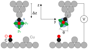
The basic tunneling junction used in the experiments and simulations is sketched in Fig. 1, where the CO-terminated tip exhibits a tilt angle subtending the surface normal in the -plane. The left panel of Fig. 1 depicts the situation for a straight CO-tip (). Besides the tilt angle (right panel), the tip–surface distance () is changed by displacing the tip (), and the voltage applied across the junction is modified. The -orbital and two -orbitals of the O atom are depicted as circles and elliptical lobes, respectively.
III.2 Adsorbed Cu atom
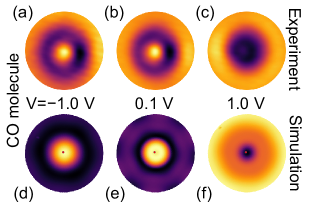
The transfer of a single CO molecule adsorbed on Cu(111) to the tip results in a CO-terminated tip with the CO axis tilted by an angle with respect to the surface normal (Fig. 1). Preparing a multitude of CO-tips gives rise to a statistical distribution of tilt angles, which are difficult to quantitatively determine from the experimental data alone. Qualitatively, the tilt angle is larger the farther the protrusions are separated in STM images of the adsorbed atom (adatom) [Fig. 2(a)–(c)]. In the following, a specific value of results from resorting to simulated topographies that best match the experimental data.
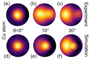
Figure 2 compares experimental [Fig. 2(a)–(c)] and calculated [Fig. 2(d)–(f)] constant-current STM images of a single Cu adatom on Cu(111) acquired with a CO tip at a given sample voltage () and with varying tilt angles (). In the experiments, the Cu adatom gives rise to a single protrusion with nearly circular circumference at [Fig. 2(a)]. Its apparent height is and full width at half maximum (FWHM) . With increasing , the STM images show two protrusions, where the larger one has an elliptical and the smaller one a circular shape. Their brightness in STM data changes with . The apparent height is and ( and ), while the FWHM (in direction, left to right in Fig. 2) is and ( and ) for the two protrusions at (). Their mutual distance increases with increasing tilt angle from at [Fig. 2(b)] to at [Fig. 2(c)].
A consistent best match of simulated STM images [Fig. 2(d)–(f)] with experimental topographies has been achieved with an ()-wave tip. While the actual absolute number for apparent heights, FWHM and protrusion separations differ from the experimental data, the observed trend is reproduced (vide infra). In particular, the shape of the adjacent protrusions for matches well the experimental observation. Other tips have likewise been tested in the simulations. The spherically symmetric O -orbital expectedly led to a single protrusion in simulated STM images of the adatom for both straight and tilted tips. The -wave tip gave rise to a double-feature contrast of the adatom in the straight-tip configuration, which was removed in the tilted-tip geometry, contrasting the experimental observation. In addition, while the DFT-derived straight CO-tip provided good agreement with experimental data (Fig. 3), its tilted counterpart failed to reproduce the observed double-feature contrast.
Imaging the single adatom with a straight -wave CO-tip gives rise to an apparent height of and an FWHM of . Upon tilting the tip, two protrusions occur in the simulated STM images with apparent heights of and ( and ), and FWHM of and ( and ) at (). The splitting of the single protrusion at increases from () to (). Using the orbital decomposition of the tunneling current discussed below, the left protrusion results from the overlap of the O -orbital with the adatom-surface wave function, while the right protrusion can be assigned to the interaction of the tilted O -orbital with the wave function of the adatom-surface hybrid.
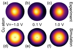
In a next step, the voltage dependence of measured and calculated STM images was explored for (Fig. 3) and (Fig. 4). The overall changes in the explored sample voltage range are small in both experimental and simulated data. Cross-sectional profiles were again used to compare apparent heights and FWHM. For in the experiments, and at were obtained [Fig. 3(a)]. At and , varies from to , while essentially stays nearly constant (). A Cu adatom imaged with a metal tip appears approximately half as high in the same voltage range. The simulations with a straight CO-tip give rise to , (), , (), and , ().
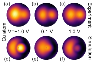
For the tilted CO-tip (Fig. 4) the apparent height of the broad protrusion decreases from at to at and , while an apparent height of for the sharp protrusion is virtually independent of the voltage. Simulated images using an ()-wave tip reproduce the evolution of the broad protrusion, with an apparent height being larger at than at and . The sharp protrusion presents a monotonic increase of from to , which is at odds with the experiment. Overall, the ()-wave tip provided the best match of the simulations with the experiments.
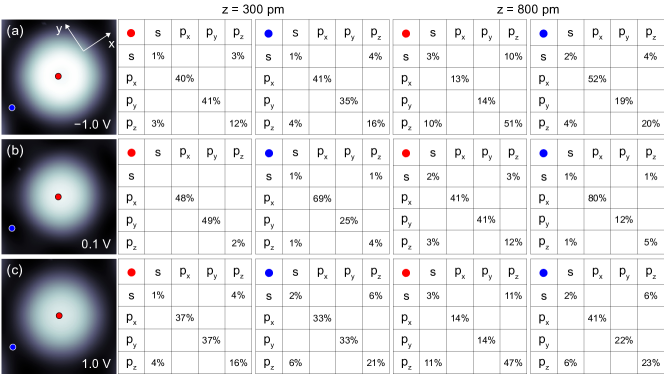
The overall good agreement between experimental and calculated data for the Cu adatom imaged with a straight CO-tip at different voltages (Fig. 3) encouraged the analysis of the tip-orbital composition of the tunneling current. To this end, the revised Chen’s method [63] was used to decompose the current in terms of the real-space electron orbitals of the O apex atom of the DFT-derived CO-tip. Figure 5 shows the results for sample voltages [Fig. 5(a)], [Fig. 5(b)], [Fig. 5(c)], and for tip–surface distances of , above two different sites (center of and separated from the adatom).
The diagonal elements of the matrices represent the contributions of each individual O orbital, while the off-diagonal elements are due to interference effects between different orbitals. This decomposition follows from the description of the Bardeen tunneling matrix element [62] as
| (1) |
where the indices , indicate sample and tip states, respectively, denotes the vacuum decay constant of tip orbital for the O atom considered here, and corresponds to the tunneling matrix element of the given orbital symmetry [63]. The differential operator acts on the sample wave function at the tip apex position and reflects the contribution of, respectively, the , , , -orbital of the O atom. While the first term in Eq. (1) is the sum over the diagonal elements of the matrices of Fig. 5 and thus reflects the direct contribution of orbitals to the tunneling current, the second term represents the sum over the off-diagonal elements that describe interference terms between different orbitals.
Above the Cu adatom center, the O -orbital contributes significantly to the current at and becomes even dominant for large tip–surface distances at these voltages. The polarity of the voltage does not affect this behavior. At , the tunneling current is instead carried by O , -orbitals, which is in line with their dominant density of states (DOS) at the Fermi energy (). These tip orbitals efficiently overlap with the , , , -orbitals of the Cu adatom, which are most important for the partial DOS of the surface. Upon increasing the tip–surface separation, at the contribution of and becomes less important for the benefit of the -orbital, which now overlaps with the , -orbital of the Cu adatom.
The split protrusion appearing when imaging the Cu adatom with a tilted CO-probe can be understood as follows. The CO-tip is tilted in the -plane along the negative -axis (Fig. 1) and scans along the -axis from negative to positive values with the Cu adatom residing at . A first protrusion in constant-current STM images develops when -orbitals of the CO molecule and the Cu adatom overlap. The CO -orbital plays a minor role because it is tilted away from the adatom site. After surmounting and passing the Cu adatom, the overlap of -orbitals reduces giving rise to a decreasing tunneling current and a concomitantly decreasing apparent height in the constant-current STM image. The apparent height increases again on the verge of interaction between the CO -orbital and the Cu atom -orbital, which for the continued scan along the -axis causes the second protrusion in the STM image.
III.3 Adsorbed CO molecule
In an effort to extend the complexity of the junction, an adsorbed CO molecule (Fig. 1) was imaged. Figure 6 shows the voltage-dependent results obtained with a straight CO-tip in the experiments [Fig. 6(a)–(c)] and simulations [Fig. 6(d)–(f)]. The adsorbed CO molecule gives rise to a circular protrusion at [Fig. 6(a)] and at [Fig. 6(b)] that is centered in a wider and likewise circular depression. The apparent height of the protrusion changes from at to at , while the depression is below the apparent height of the Cu(111) surface. At [Fig. 6(c)], the central protrusion almost disappears. Its apparent height is below the apparent Cu(111) surface height. The diameter of the circular depression stays nearly constant () for the range of applied sample voltages.
The experimental data at can be best reproduced in the simulations by using an -wave tip. In particular, the transition of the pronounced central protrusion at [Fig. 6(d)] to a depression at [Fig. 6(f)] is well captured only with the -wave tip. The DFT-derived CO-tip reproduces the experimental contrast at with a larger FWHM (not shown) but is unable to show the depression at . At [Fig. 6(e)] both the -wave and the DFT-derived CO-tip provide simulated STM images that are in accordance with experimental data. The increase of the apparent height from at to at reflects the same trend observed in the experiments.
For adsorbed CO, constant-height mapping of the tunneling current at decreasing tip–surface distances was achieved [Fig. 7(a)–(e)], which in the case of the Cu adatom was impeded due to its tip-induced lateral diffusion already at elevated tip–surface separations. The experimental data show that a decrease of the tip–surface distance from the far tunneling range [, Fig. 7(a)] by [Fig. 7(b)] leads to a contrast increase of the central protrusion from to . Concomitantly, the contrast due to the Cu(111) surface increases only from to . The FWHM of the central protrusion, however, stays nearly constant (). Further decrease of the tip–surface separation entails strong changes in the appearance of the adsorbed CO molecule. The central protrusion has considerably widened [FWHM at , Fig. 7(c)] and exhibits a substructure with two adjacent maxima separated by a thin low-contrast line. Most likely, the two CO molecules are already so close to each other that the interaction causes their bending [50, 65]. These relaxations of the junction geometry become more pronounced with decreasing CO–CO distance [Fig. 7(d),(e)]. The sharp edges confining the central protrusion are indicative of bond formation between the opposing CO molecules in the junction. The conjectured junction relaxations leave their fingerprint in current-versus-displacement traces, too [Fig. 7(f)]. The depicted data were extracted from the central region of the constant-height current maps. A deviation from a uniform exponential increase of the current occurs in a tip displacement range , which matches well the range where image distortions are first observed.
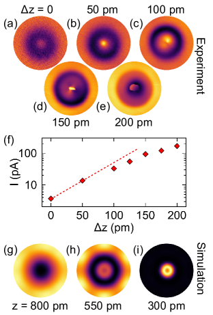
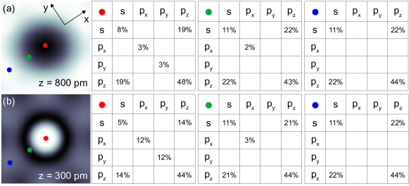
The simulations reported here do not take such junction relaxations and CO–CO interactions into account. Therefore, calculations of constant-height STM images are restricted to the tunneling range of electrode separations. In the far tunneling range (), the adsorbed CO molecule appears as a depression [Fig. 7(g)], which at smaller tip–surface distances [, Fig. 7(h) and , Fig.7(i)] is transformed into an increasingly sharp central protrusion embedded in the wider depression. This contrast evolution can be well compared with the experimental observations in the tunneling range [ and in Fig. 7(a),(b)]. The sharp central indentation of contrast is most likely due to the overlap of ,-orbitals in the CO–CO junction at small distance reflecting the node of the -orbitals. A lateral displacement of the CO-probe from the aligned CO–CO configuration then leads to a finite overlap of these orbitals and the concomitant increase of the tunneling current. The orbital decomposition of the current (Fig. 8) indeed shows that the contribution of ,-orbitals becomes indeed larger at small CO–CO separations.
For two tip–surface distances (), the orbital composition of the tunneling current was computed for the straight DFT-derived CO-tip (Fig. 8). In the far tunneling range of tip–surface separations [Fig. 8(a)], the -orbital of the O atom gives the dominant direct contribution to the tunneling current at all considered tip positions [dots in Fig. 8(a)]. Likewise, / interference terms contribute strongly. Small amounts of the tunneling current are carried by the , , -orbitals atop the CO center. They essentially even vanish upon laterally positioning the CO-terminated tip to the sides of the adsorbed CO molecule. While , -orbitals exhibit the highest projected DOS of the O atom at , the orientation of the -orbital and its vacuum decay obviously play the key role in determining the magnitude of the tunneling current. At decreased tip–surface distance [, Fig. 8(b)], the , -orbitals contribute more strongly to the tunneling current, at the expense of the interference terms.
Before concluding it is noteworthy that simulations with a tilted CO-tip and upright adsorbed CO were likewise performed (not shown). However, agreement between experimental and calculated data was difficult to achieve with this assumed junction geometry. Therefore, the weak-coupling limit used for the modeling reported here is not applicable to these junctions. Rather, an increased CO–CO interaction becomes important, which is evidenced by the experimental data.
IV Conclusion
The Chen’s derivative rules have successfully been applied to describe experimental STM images acquired with a CO-terminated tip of an adsorbed Cu atom and CO molecule on Cu(111). For the adatom junction, the dependence of topographies on voltage and CO-probe tilt angle can be traced to the orientation of specific tip orbitals and their overlap with the wave function of the adatom-surface hybrid. In case of the CO–CO junction, the impact of the imaging voltage as well as the CO–CO distance are captured in the weak-interaction limit and for the straight geometry. In all junctions, interference terms are important for describing experimental STM images. Increased intermolecular coupling at small mutual distance that induces relaxations of the junction require further development of state-of-the-art simulation methods.
Acknowledgements.
Financial support from the National Research Development and Innovation Office of Hungary (NKFIH, Grant No. FK124100), a Stipendium Hungaricum Scholarship of the Tempus Public Foundation, the János Bolyai Research Grant of the Hungarian Academy of Sciences (Grant No. BO/292/21/11), the New National Excellence Program of the Ministry for Culture and Innovation from NKFIH Fund (Grant Nos. ÚNKP-22-5-BME-282, ÚNKP-23-5-BME-12) and from the Deutsche Forschungsgemeinschaft through KR 2912/17-1 is acknowledged.References
- Ruan et al. [1993] L. Ruan, F. Besenbacher, I. Stensgaard, and E. Laegsgaard, Atom resolved discrimination of chemically different elements on metal surfaces, Phys. Rev. Lett. 70, 4079 (1993).
- Bartels et al. [1998] L. Bartels, G. Meyer, K.-H. Rieder, D. Velic, E. Knoesel, A. Hotzel, M. Wolf, and G. Ertl, Dynamics of electron-induced manipulation of individual CO molecules on Cu(111), Phys. Rev. Lett. 80, 2004 (1998).
- Repp et al. [2005] J. Repp, G. Meyer, S. M. Stojković, A. Gourdon, and C. Joachim, Molecules on insulating films: Scanning-tunneling microscopy imaging of individual molecular orbitals, Phys. Rev. Lett. 94, 026803 (2005).
- Repp et al. [2006] J. Repp, G. Meyer, S. Paavilainen, F. E. Olsson, and M. Persson, Imaging bond formation between a gold atom and pentacene on an insulating surface, Science 312, 1196 (2006).
- Liljeroth et al. [2007] P. Liljeroth, J. Repp, and G. Meyer, Current-induced hydrogen tautomerization and conductance switching of naphthalocyanine molecules, Science 317, 1203 (2007).
- Gross et al. [2011] L. Gross, N. Moll, F. Mohn, A. Curioni, G. Meyer, F. Hanke, and M. Persson, High-resolution molecular orbital imaging using a -wave STM tip, Phys. Rev. Lett. 107, 086101 (2011).
- Gross [2011] L. Gross, Recent advances in submolecular resolution with scanning probe microscopy, Nat. Chem. 3, 273 (2011).
- Jelínek [2017] P. Jelínek, High resolution SPM imaging of organic molecules with functionalized tips, J. Phys.: Condens. Matter 29, 343002 (2017).
- Bischoff et al. [2018] F. Bischoff, Y. He, A. Riss, K. Seufert, W. Auwärter, and J. V. Barth, Exploration of interfacial porphine coupling schemes and hybrid systems by bond-resolved scanning probe microscopy, Angew. Chem. Int. Ed. 57, 16030 (2018).
- Su et al. [2019] J. Su, M. Telychko, P. Hu, G. Macam, P. Mutombo, H. Zhang, Y. Bao, F. Cheng, Z.-Q. Huang, Z. Qiu, S. J. R. Tan, H. Lin, P. Jelínek, F.-C. Chuang, J. Wu, and J. Lu, Atomically precise bottom-up synthesis of -extended [5]triangulene, Sci. Adv. 5, eaav7717 (2019).
- Lohr et al. [2020] T. G. Lohr, J. I. Urgel, K. Eimre, J. Liu, M. Di Giovannantonio, S. Mishra, R. Berger, P. Ruffieux, C. A. Pignedoli, R. Fasel, and X. Feng, On-surface synthesis of non-benzenoid nanographenes by oxidative ring-closure and ring-rearrangement reactions, J. Am. Chem. Soc. 142, 13565 (2020).
- Mallada et al. [2021a] B. Mallada, B. de la Torre, J. I. Mendieta-Moreno, D. Nachtigallová, A. Matěj, M. Matoušek, P. Mutombo, J. Brabec, L. Veis, T. Cadart, M. Kotora, and P. Jelínek, On-surface strain-driven synthesis of nonalternant non-benzenoid aromatic compounds containing four- to eight-membered rings, J. Am. Chem. Soc. 143, 14694 (2021a).
- Fan et al. [2021] Q. Fan, L. Yan, M. W. Tripp, O. Krejčí, S. Dimosthenous, S. R. Kachel, M. Chen, A. S. Foster, U. Koert, P. Liljeroth, and J. M. Gottfried, Biphenylene network: A nonbenzenoid carbon allotrope, Science 372, 852 (2021).
- Song et al. [2021] S. Song, J. Su, X. Peng, X. Wu, and M. Telychko, Recent advances in bond-resolved scanning tunneling microscopy, Surf. Rev. Lett. 28, 2140007 (2021).
- Lawrence et al. [2022] J. Lawrence, A. Berdonces-Layunta, S. Edalatmanesh, J. Castro-Esteban, T. Wang, A. Jimenez-Martin, B. de la Torre, R. Castrillo-Bodero, P. Angulo-Portugal, M. S. G. Mohammed, A. Matěj, M. Vilas-Varela, F. Schiller, M. Corso, P. Jelinek, D. Peña, and D. G. de Oteyza, Circumventing the stability problems of graphene nanoribbon zigzag edges, Nat. Chem. 14, 1451 (2022).
- Yang et al. [2022] X.-Q. Yang, J.-J. Duan, J. Su, X. Peng, Z.-Y. Yi, R.-N. Li, J. Lu, S.-F. Wang, T. Chen, and D. Wang, Aromatic ring fusion to benzoporphyrin via -ortho cyclodehydrogenation on a Ag(111) surface, ACS Nano 16, 13092 (2022).
- Rascon et al. [2023] E. C. Rascon, A. Riss, A. Matěj, A. Wiengarten, P. Mutombo, D. Soler, P. Jelinek, and W. Auwärter, On-surface synthesis of square-type porphyrin tetramers with central antiaromatic cyclooctatetraene moiety, J. Am. Chem. Soc. 145, 967 (2023).
- Néel and Kröger [2023] N. Néel and J. Kröger, Orbital and skeletal structure of a single molecule on a metal surface unveiled by scanning tunneling microscopy, The Journal of Physical Chemistry Letters 14, 3946 (2023).
- Temirov et al. [2008] R. Temirov, S. Soubatch, O. Neucheva, A. C. Lassise, and F. S. Tautz, A novel method achieving ultra-high geometrical resolution in scanning tunnelling microscopy, New J. Phys. 10, 053012 (2008).
- Weiss et al. [2010] C. Weiss, C. Wagner, C. Kleimann, M. Rohlfing, F. S. Tautz, and R. Temirov, Imaging Pauli repulsion in scanning tunneling microscopy, Phys. Rev. Lett. 105, 086103 (2010).
- Kichin et al. [2011] G. Kichin, C. Weiss, C. Wagner, F. S. Tautz, and R. Temirov, Single molecule and single atom sensors for atomic resolution imaging of chemically complex surfaces, J. Am. Chem. Soc. 133, 16847 (2011).
- Gross et al. [2009] L. Gross, F. Mohn, N. Moll, P. Liljeroth, and G. Meyer, The chemical structure of a molecule resolved by atomic force microscopy, Science 325, 1110 (2009).
- Gross et al. [2010] L. Gross, F. Mohn, N. Moll, G. Meyer, R. Ebel, W. M. Abdel-Mageed, and M. Jaspars, Organic structure determination using atomic-resolution scanning probe microscopy, Nat. Chem. 2, 821 (2010).
- Gross et al. [2012] L. Gross, F. Mohn, N. Moll, B. Schuler, A. Criado, E. Guitián, D. Peña, A. Gourdon, and G. Meyer, Bond-order discrimination by atomic force microscopy, Science 337, 1326 (2012).
- de Oteyza et al. [2013] D. G. de Oteyza, P. Gorman, Y.-C. Chen, S. Wickenburg, A. Riss, D. J. Mowbray, G. Etkin, Z. Pedramrazi, H.-Z. Tsai, A. Rubio, M. F. Crommie, and F. R. Fischer, Direct imaging of covalent bond structure in single-molecule chemical reactions, Science 340, 1434 (2013).
- Hämäläinen et al. [2014] S. K. Hämäläinen, N. van der Heijden, J. van der Lit, S. den Hartog, P. Liljeroth, and I. Swart, Intermolecular contrast in atomic force microscopy images without intermolecular bonds, Phys. Rev. Lett. 113, 186102 (2014).
- Sweetman et al. [2014] A. M. Sweetman, S. P. Jarvis, H. Sang, I. Lekkas, P. Rahe, Y. Wang, J. Wang, N. Champness, L. Kantorovich, and P. Moriarty, Mapping the force field of a hydrogen-bonded assembly, Nat. Commun. 5, 3931 (2014).
- Mönig et al. [2016] H. Mönig, D. R. Hermoso, O. Díaz Arado, M. Todorović, A. Timmer, S. Schüer, G. Langewisch, R. Pérez, and H. Fuchs, Submolecular imaging by noncontact atomic force microscopy with an oxygen atom rigidly connected to a metallic probe, ACS Nano 10, 1201 (2016).
- Kawai et al. [2017] S. Kawai, T. Nishiuchi, T. Kodama, P. Spijker, R. Pawlak, T. Meier, J. Tracey, T. Kubo, E. Meyer, and A. S. Foster, Direct quantitative measurement of the CO H–C bond by atomic force microscopy, Sci. Adv. 3, e1603258 (2017).
- Mallada et al. [2021b] B. Mallada, A. Gallardo, M. Lamanec, B. de la Torre, V. Špirko, P. Hobza, and P. Jelinek, Real-space imaging of anisotropic charge of -hole by means of kelvin probe force microscopy, Science 374, 863 (2021b).
- Chutora et al. [2019] T. Chutora, B. de la Torre, P. Mutombo, J. Hellerstedt, J. Kopeček, P. Jelínek, and M. Švec, Nitrous oxide as an effective afm tip functionalization: a comparative study, Beilstein Journal of Nanotechnology 10, 315 (2019).
- Hapala et al. [2014] P. Hapala, G. Kichin, C. Wagner, F. S. Tautz, R. Temirov, and P. Jelínek, Mechanism of high-resolution STM/AFM imaging with functionalized tips, Phys. Rev. B 90, 085421 (2014).
- Néel and Kröger [2021] N. Néel and J. Kröger, Atomic force extrema induced by the bending of a co-functionalized probe, Nano Lett. 21, 2318 (2021).
- Baumann et al. [2015] S. Baumann, W. Paul, T. Choi, C. P. Lutz, A. Ardavan, and A. J. Heinrich, Electron paramagnetic resonance of individual atoms on a surface, Science 350, 417 (2015).
- Schneider et al. [2021] L. Schneider, P. Beck, J. Wiebe, and R. Wiesendanger, Atomic-scale spin-polarization maps using functionalized superconducting probes, Science Advances 7, eabd7302 (2021).
- Czap et al. [2019] G. Czap, P. J. Wagner, F. Xue, L. Gu, J. Li, J. Yao, R. Wu, and W. Ho, Probing and imaging spin interactions with a magnetic single-molecule sensor, Science 364, 670 (2019).
- Verlhac et al. [2019] B. Verlhac, N. Bachellier, L. Garnier, M. Ormaza, P. Abufager, R. Robles, M.-L. Bocquet, M. Ternes, N. Lorente, and L. Limot, Atomic-scale spin sensing with a single molecule at the apex of a scanning tunneling microscope, Science 366, 623 (2019).
- Hahn and Ho [2001] J. R. Hahn and W. Ho, Single molecule imaging and vibrational spectroscopy with a chemically modified tip of a scanning tunneling microscope, Phys. Rev. Lett. 87, 196102 (2001).
- Teobaldi et al. [2007] G. Teobaldi, M. Peñalba, A. Arnau, N. Lorente, and W. A. Hofer, Including the probe tip in theoretical models of inelastic scanning tunneling spectroscopy: CO on Cu(100), Phys. Rev. B 76, 235407 (2007).
- Garcia-Lekue et al. [2011] A. Garcia-Lekue, D. Sanchez-Portal, A. Arnau, and T. Frederiksen, Simulation of inelastic electron tunneling spectroscopy of single molecules with functionalized tips, Phys. Rev. B 83, 155417 (2011).
- Pavliček et al. [2013] N. Pavliček, I. Swart, J. Niedenführ, G. Meyer, and J. Repp, Symmetry dependence of vibration-assisted tunneling, Phys. Rev. Lett. 110, 136101 (2013).
- Okabayashi et al. [2016] N. Okabayashi, A. Gustafsson, A. Peronio, M. Paulsson, T. Arai, and F. J. Giessibl, Influence of atomic tip structure on the intensity of inelastic tunneling spectroscopy data analyzed by combined scanning tunneling spectroscopy, force microscopy, and density functional theory, Phys. Rev. B 93, 165415 (2016).
- Meierott et al. [2016] S. Meierott, N. Néel, and J. Kröger, Spectroscopic line shapes of vibrational quanta in the presence of molecular resonances, J. Phys. Chem. Lett. 7, 2388 (2016).
- Han et al. [2017] Z. Han, G. Czap, C. Xu, C.-l. Chiang, D. Yuan, R. Wu, and W. Ho, Probing intermolecular coupled vibrations between two molecules, Phys. Rev. Lett. 118, 036801 (2017).
- de la Torre et al. [2017] B. de la Torre, M. Švec, G. Foti, O. c. v. Krejčí, P. Hapala, A. Garcia-Lekue, T. Frederiksen, R. Zbořil, A. Arnau, H. Vázquez, and P. Jelínek, Submolecular resolution by variation of the inelastic electron tunneling spectroscopy amplitude and its relation to the AFM/STM signal, Phys. Rev. Lett. 119, 166001 (2017).
- Mehler et al. [2018] A. Mehler, N. Néel, M.-L. Bocquet, and J. Kröger, Exciting Vibrons in both Frontier Orbitals of a Single Hydrocarbon Molecule on Graphene, Journal of Physics: Condensed Matter 31, 065001 (2018).
- Tersoff and Hamann [1983] J. Tersoff and D. R. Hamann, Theory and application for the scanning tunneling microscope, Phys. Rev. Lett. 50, 1998 (1983).
- Tersoff and Hamann [1985] J. Tersoff and D. R. Hamann, Theory of the Scanning Tunneling Microscope, Phys. Rev. B 31, 805 (1985).
- Néel et al. [2024] N. Néel, C. Dreßler, and J. Kröger, Effect of orbital symmetry on probing the single-molecule kondo effect, Phys. Rev. B 109, L241401 (2024).
- Sun et al. [2011] Z. Sun, M. P. Boneschanscher, I. Swart, D. Vanmaekelbergh, and P. Liljeroth, Quantitative atomic force microscopy with carbon monoxide terminated tips, Phys. Rev. Lett. 106, 046104 (2011).
- Huber et al. [2019] F. Huber, J. Berwanger, S. Polesya, S. Mankovsky, H. Ebert, and F. J. Giessibl, Chemical bond formation showing a transition from physisorption to chemisorption, Science 366, 235 (2019).
- Rothe et al. [2022a] K. Rothe, N. Néel, M.-L. Bocquet, and J. Kröger, Tracking the interaction between a CO-functionalized probe and two Ag-phthalocyanine conformers by local vertical force spectroscopy, The Journal of Physical Chemistry A 126, 6890 (2022a).
- Hauptmann et al. [2015] N. Hauptmann, L. Groß, K. Buchmann, K. Scheil, C. Schütt, F. L. Otte, R. Herges, C. Herrmann, and R. Berndt, High-conductance surface-anchoring of a mechanically flexible platform-based porphyrin complex, New Journal of Physics 17, 013012 (2015).
- Brand et al. [2019a] J. Brand, N. Néel, and J. Kröger, Probing relaxations of atomic-scale junctions in the Pauli repulsion range, New Journal of Physics 21, 103041 (2019a).
- Brand et al. [2019b] J. Brand, S. Leitherer, N. R. Papior, N. Néel, Y. Lei, M. Brandbyge, and J. Kröger, Nonequilibrium bond forces in single-molecule junctions, Nano Letters 19, 7845 (2019b).
- Berwanger et al. [2020] J. Berwanger, S. Polesya, S. Mankovsky, H. Ebert, and F. J. Giessibl, Atomically resolved chemical reactivity of small Fe clusters, Phys. Rev. Lett. 124, 096001 (2020).
- Wagner et al. [2021] M. Wagner, B. Meyer, M. Setvin, M. Schmid, and U. Diebold, Direct assessment of the acidity of individual surface hydroxyls, Nature 592, 722 (2021).
- Rothe et al. [2022b] K. Rothe, N. Néel, M.-L. Bocquet, and J. Kröger, Quantifying force and energy in single-molecule metalation, J. Am. Chem. Soc. 144, 7054 (2022b).
- Rothe et al. [2022c] K. Rothe, N. Néel, M.-L. Bocquet, and J. Kröger, Extraction of chemical reactivity and structural relaxations of an organic dye from the short-range interaction with a molecular probe, J. Phys. Chem. Lett. 13, 8660 (2022c).
- Siegert et al. [2013] B. Siegert, A. Donarini, and M. Grifoni, The role of the tip symmetry on the STM topography of -conjugated molecules, Phys. Status Solidi B 250, 2444 (2013).
- Chen [1990] C. J. Chen, Tunneling matrix elements in three-dimensional space: The derivative rule and the sum rule, Phys. Rev. B 42, 8841 (1990).
- Bardeen [1961] J. Bardeen, Tunnelling from a many-particle point of view, Phys. Rev. Lett. 6, 57 (1961).
- Mándi and Palotás [2015] G. Mándi and K. Palotás, Chen’s derivative rule revisited: Role of tip-orbital interference in STM, Phys. Rev. B 91, 165406 (2015).
- Gustafsson and Paulsson [2016] A. Gustafsson and M. Paulsson, Scanning tunneling microscopy current from localized basis orbital density functional theory, Phys. Rev. B 93, 115434 (2016).
- Gustafsson et al. [2017] A. Gustafsson, N. Okabayashi, A. Peronio, F. J. Giessibl, and M. Paulsson, Analysis of stm images with pure and co-functionalized tips: A first-principles and experimental study, Phys. Rev. B 96, 085415 (2017).
- Mándi et al. [2013] G. Mándi, N. Nagy, and K. Palotás, Arbitrary tip orientation in STM simulations: 3D WKB theory and application to W(110), Journal of Physics: Condensed Matter 25, 445009 (2013).
- Mándi et al. [2014] G. Mándi, G. Teobaldi, and K. Palotás, Contrast stability and ‘stripe’ formation in scanning tunnelling microscopy imaging of highly oriented pyrolytic graphite: the role of STM-tip orientations, Journal of Physics: Condensed Matter 26, 485007 (2014).
- Mándi et al. [2015] G. Mándi, G. Teobaldi, and K. Palotás, What is the orientation of the tip in a scanning tunneling microscope?, Progress in Surface Science 90, 223 (2015).
- Limot et al. [2005] L. Limot, J. Kröger, R. Berndt, A. Garcia-Lekue, and W. A. Hofer, Atom transfer and single-adatom contacts, Phys. Rev. Lett. 94, 126102 (2005).
- Kröger et al. [2007] J. Kröger, H. Jensen, and R. Berndt, Conductance of tip–surface and tip–atom junctions on Au(111) explored by a scanning tunnelling microscope, New J. Phys. 9, 153 (2007).
- Kröger et al. [2009] J. Kröger, N. Néel, A. Sperl, Y. F. Wang, and R. Berndt, Single-atom contacts with a scanning tunnelling microscope, New J. Phys. 11, 125006 (2009).
- Kröger et al. [2008] J. Kröger, N. Néel, and L. Limot, Contact to single atoms and molecules with the tip of a scanning tunnelling microscope, J. Phys.: Condens. Matter 20, 223001 (2008).
- Néel et al. [2009] N. Néel, J. Kröger, and R. Berndt, Quantized conductance of a single magnetic atom, Phys. Rev. Lett. 102, 086805 (2009).
- Berndt et al. [2010] R. Berndt, J. Kröger, N. Néel, and G. Schull, Controlled single atom and single molecule contacts, Phys. Chem. Chem. Phys. 12, 1022 (2010).
- Bartels et al. [1997] L. Bartels, G. Meyer, and K.-H. Rieder, Controlled vertical manipulation of single CO molecules with the scanning tunneling microscope: A route to chemical contrast, Appl. Phys. Lett. 71, 213 (1997).
- Horcas et al. [2007] I. Horcas, R. Fernández, J. M. Gómez-Rodríguez, J. Colchero, J. Gómez-Herrero, and A. M. Baro, Wsxm: A software for scanning probe microscopy and a tool for nanotechnology, Rev. Sci. Instrum. 78, 013705 (2007).
- Kresse and Furthmüller [1996] G. Kresse and J. Furthmüller, Efficient iterative schemes for ab initio total-energy calculations using a plane-wave basis set, Phys. Rev. B 54, 11169 (1996).
- Perdew et al. [1996] J. P. Perdew, K. Burke, and M. Ernzerhof, Generalized gradient approximation made simple, Phys. Rev. Lett. 77, 3865 (1996).
- Kresse and Joubert [1999] G. Kresse and D. Joubert, From ultrasoft pseudopotentials to the projector augmented-wave method, Phys. Rev. B 59, 1758 (1999).
- Breeman et al. [1995] M. Breeman, G. Barkema, and D. Boerma, Binding energies and stability of Cu-adatom clusters on Cu(100) and Cu(111), Surface Science 323, 71 (1995).
- ichi Ishi et al. [1985] S. ichi Ishi, Y. Ohno, and B. Viswanathan, An overview on the electronic and vibrational properties of adsorbed co, Surface Science 161, 349 (1985).
- Monkhorst and Pack [1976] H. J. Monkhorst and J. D. Pack, Special points for Brillouin-zone integrations, Phys. Rev. B 13, 5188 (1976).
- Hofer [2003] W. Hofer, Challenges and errors: interpreting high resolution images in scanning tunneling microscopy, Progress in Surface Science 71, 147 (2003).
- Palotas and Hofer [2005] K. Palotas and W. Hofer, Multiple scattering in a vacuum barrier obtained from real-space wavefunctions, J. Phys.: Condens. Matter 17, 2705 (2005).