Further author information: (Send correspondence to R.S.)
R.S.: E-mail: ranjani.srinivasan@cfa.harvard.edu
The Black Hole Explorer: Back End Electronics
Abstract
This paper describes specification and early design of back end signal processing subsystems for the Black Hole Explorer (BHEX) Very Long Baseline Interferometry (VLBI) space telescope. The“back end” consists of two subsystems. First, the block downconveter (BDC) is a heterodyne system that performs a frequency translation of the analog signal from IF to baseband and amplifies and filters it for digitization. Second, the digital back end (DBE) samples the analog signal with an analog-to-digital converters (ADC) and digitally processes the data stream formatting them to the VLBI “VDIF” standard and converting to Ethernet packets for 100 gigabit-per-second (Gb/s) Ethernet transport to the optical downlink system [1]. Both the BDC and the DBE for BHEX support eight channels of 4.096 GHz bandwidth each, for a total processed bandwidth of 32.768 GHz. The BHEX back end benefits from mature terrestrial back end heritage, described in some detail. The BHEX back end itself is in the early stages of design, with requirements, interface specifications, and component trade studies well advanced. The aim is to build a prototype using terrestrial grade parts which are available in functionally identical space grade equivalents, and to use this prototype to advance the back end Technology Readiness Level (TRL) preparing for a Small Explorer (SMEX) proposal in 2025.
keywords:
Radio Astronomy, Instrumentation, Digital Signal Processing, VLBI, BHEX, Photon Ring1 INTRODUCTION
The Black Hole Explorer (BHEX) [2] is a 1 mm Very Long Baseline Interferometry (VLBI) station in a mid-Earth orbit (MEO). BHEX will discover, measure, and make images of the bright and narrow “photon ring” that is predicted to exist around black holes. The photon ring corresponds to light that has circled the black hole—sometimes multiple times—before escaping, and is a fine structure underlying the Event Horizon Telescope (EHT) black hole ring images of M87* [3], and SgrA* [4]. Making an image of the photon ring is not possible on terrestrial EHT baselines which are limited to one earth diameter. BHEX extends the EHT to space allowing the baseline length, and enabling the necessary resolution. This paper presents a description and initial design of BHEX signal processing elements following the dual receivers [5] and prior to the optical data downlink system.[6],[1]
Section 2 briefly describes the BHEX electronics, and section 3 describes progenitor terrestrial back end systems. The BHEX back end work includes trade studies, requirements and interface development, and firmware design, and is described in section 4. The first objective is a prototype, built with terrestrial equivalents of space grade parts, used for functional and environmental testing and TRL maturation, to prepare for a SMEX mission proposal in 2025.
2 BHEX System Overview
The major subsystems of the BHEX science instrument are a 3.5 meter antenna. The antenna is coupled to a coherent dual band, dual-polarization receiver, then to the back end described in this paper which in turn feeds dat to a high throughput optical downlink [1]. We provide a brief description of the BHEX subsystems other than the back end as context for the latter’s detailed description in section 4. For more detail of the entire instrument please see the relevant companion paper in this proceedings [9].
2.1 Dish Antenna
As the space-based component of a space-ground interferometer, the sensitivity of each space-ground baseline (formed by correlating the electric fields received simultaneously at BHEX and a ground-based observatory) is proportional to the geometric mean of the space and ground antenna collecting areas. This allows BHEX to be implemented with a 3.5 m dish [16] suitable for launch in available fairings.
2.2 Dual Band Receivers
The receivers [5] observe simultaneously in two bands. The “low” band is centered at 86 GHz. The “high” band has a center frequency widely tunable between 220 and 325 GHZ. Each receiver has wide sidebands of 8.192 GHz, and both polarizations are detected, so each band has a total width of 16.384 GHz—32.768 GHz across both receivers. The wide bandwidth improves signal-to-noise-ratio (SNR) according to the radiometer equation, but results in large data payloads which are a challenge to downlink. 111The receiver for the high band is a so-called “double sideband” or DSB architecture, meaning that two sidebands (upper and lower) on the sky are overlaid onto a single receiver IF output. Thus the total dual band sky frequency coverage is in fact 32.768 GHz. The upper and lower sidebands are separated at the terrestrial VLBI correlator after data downlink. The DSB approach aims to reduce downlink payload for this very wide sky bandwidth which is invisible to the back end electronics, and “sees” the unseparated 16.384 GHz bandwidth. The low band receiver is a single sideband (USB) system with dual polarization.. The receivers operate at cryogenic temperatures, the high band requiring a cold stage of 4 K. Space qualified cryogenics are specialized systems discussed in a companion paper in this proceedings [17].
The effect of the atmosphere on the phase of the wavefront received at ground stations increases with frequency resulting in significant coherence losses at high observing frequencies. A major motivation for BHEX and its associated ground array to observe simultaneously in two bands, is to enable Frequency Phase Transfer (FPT) [13]. FPT transfers phase calibration from the low band to the high band. The low band has greater sensitivity and is less affected by the atmosphere, however low band VLBI even on the BHEX array long base baseline has insufficient resolution to resolve the photon ring. The primary purpose of the low band is to provide a phase calibration of the high band whose short wavelength results in fine angular resolution sufficient to resolve the photon ring. Also in the case of SgrA* the high band sees more clearly to the core of the source, and the image is less blurred by scattering in the interstellar medium foreground.
2.3 Frequency reference
An ultra-stable oscillator provides the master frequency reference, to ensure coherence of the BHEX space station on timescales sufficient to find correlation detections, or “fringes”. Both quartz oscillators and a new breed of compact iodine atomic clocks are in consideration for this critical subsystem function.
2.4 Optical Data Downlink
The TBIRD (TeraByte Infrared Delivery) is a small cubesat mission in low-earth orbit (LEO) and recently (2022, 2023)[6] demonstrated up to 200 Gb/s downlink capacity. This is far more data than available from typical radio-frequency links or prior space optical communications. The Optical Data Downlink subsystem under development for BHEX is the evolution of the TBIRD system and is discussed in detail in companion papers in this proceedings [9], [1]. The optical downlink subsystem lies immediately downstream of the BHEX DBE, which is one of the two subsystems described in detail in the present paper.
3 Progenitor Terrestrial Back End Subsystems
The development of the BHEX back end subsystems benefit from considerable terrestrial experience developing EHT back ends subsystems. Our Digital Signal Processing (DSP) team at the Smithsonian Astrophysical Observatory (SAO) has considerable experience in the application of wideband samplers (or analog-to-digital converters, ADC) and FPGAs in the design of signal processing systems for ground-based submillimeter interferometry. We have designed and commissioned the terrestrial back ends for the Event Horizon Telescope (EHT)[18] and correlator-beamformer systems for the Submillimeter Array (SMA) [19].
Back ends for the next generation Event Horizon Telescope (ngEHT) [20] capable of conditioning and simultaneously digitizing 4 x 8.192 GHz of instantaneous analog bandwidth are in advanced development. The ngEHT back end comprises an analog signal processing component (ngBDC) and a digitizer and digital signal processor board (ngDBE). The ngDBE development includes a considerable library of firmware for ADC interfacing, signal processing, and an Ethernet stack. The ngEHT design including both hardware and firmware elements provides considerable experience and heritage benefiting the design of the BHEX back ends.
The installed and commissioned EHT back ends are discussed in 3.1, and the next generation back end subsystems in sections 3.2 and 3.3. The ngDBE FPGA firmware is discussed in 3.4 noting that the considerable effort in this firmware can readily be leveraged and ported to the BHEX DBE.
3.1 ROACH2 Digital Back End (R2DBE)
The current EHT back end was developed in 2014, and is called the ROACH2 Digital Back End [18, R2DBE]. The R2DBE samples 2 x 2.048 GHz of instantaneous analog bandwidth. It uses a Xilinx Virtex 6 FPGA as its digital signal processing engine to re-quantize 8-bit samples to 2-bit resolution, pack the data in VDIF format, and transmit them over two 10 Gb/s Ethernet connections to the data recorder. Accurate timing and synchronization is achieved by referencing to a hydrogen maser. The ngDBE has a matching block downconverter (BDC) developed in Europe at NOVA Laboratories. The R2DBE was successfully deployed to all single-dish EHT telescopes that observed in 2017, resulting in the first EHT images of M87*[3] and SgrA*[21].
3.2 next generation Block Downconverter (ngBDC)
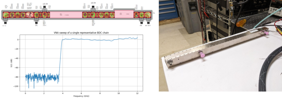
The ngBDC performs a frequency translation of the receiver output from IF to baseband and conditions it for digitization by the ngDBE. For simultaneous tri frequency, dual polarization and dual sideband operations, twelve such signal processing chains are required. The prototype was manufactured by Xmicrowave, Inc, using drop-in modules representative of the final ngBDC circuit board. The prototype was characterized and performance was found to be well within the specifications. The prototype was converted to a production custom printed circuit board in a fieldable enclosure. Shown in Figure 1 are layout of the production unit (with the two custom filters seen) on the top left panel, a photo of the production version housed in an EMI enclosure (right panel) and a VNA sweep of a representative signal chain (bottom left panel), the performance across the passband looks excellent.
The design incorporates the following features:
-
1.
A sophisticated downconversion scheme employing an “up-down” conversion method to eliminate mixing of input and output signals.
-
2.
Test points using input and output stage couplers to help with debugging.
-
3.
Two custom filters to provide image rejection and to provide a sharp Nyquist cutoff to prevent aliasing.
-
4.
Second stage mixing using spectral inversion.
-
5.
An input stage closed loop servo control using a Variable Voltage Attenuator (VVA) to prevent any compression arising from higher input power levels.
-
6.
An output stage open loop Automatic Gain Control (AGC) using a VVA to load the digitizer optimally.
The field deployable units are modular in design with respect to frequency which will allow for ease of installation and future expansion.
3.3 next generation Digital Back End (ngDBE)
Each ngDBE board accepts four 8.192 GHz baseband inputs. The Nyquist criterion for sampling requires sampling the data at 16.384 Gsps. Each ngDBE board is outfitted with four 4-bit high speed wideband analog to digital converters from Adsantec and a VU13P, an Ultrascale+ Virtex FPGA from AMD Xilinx and other ancilliary components. Two 64 Gbps streams of packetized 2-bit data are sent out to be shipped over 100 GbE interfaces to recorders.
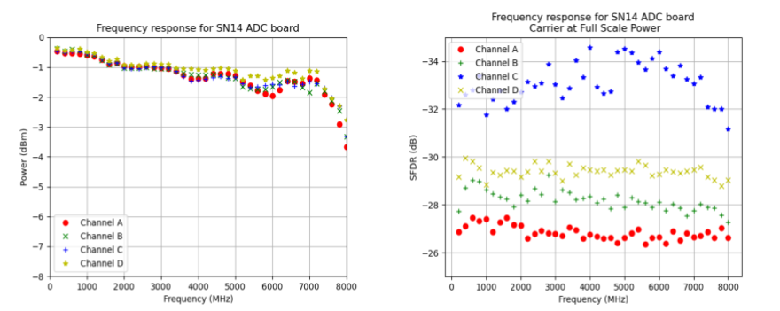
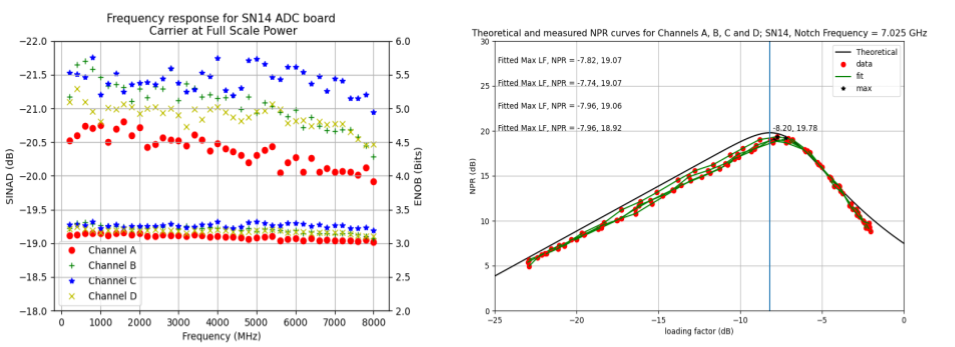
The high speed analog to digital converters were fully characterized, and several relevant figures of merit are measured and compared to theoretical expectations. The frequency response of the ADC and Spurious Free Dynamic Range (SFDR) measurements are plotted in Figure 2. The frequency response is very flat with only a 3 dB slope across the 8 GHz passband. Similarly the SFDR is well within expected levels for such a wideband ADC. The other two key figures of merit namely the Effective Number of Bits (ENOB), which is derived from SIgnal to Noise And Distortion (SINAD) and the Noise Power ratio (NPR) are shown in Figure 3 on the left and right panels respectively. The ENOB stays above 3 bits and above across the entire band. We consider this performance quite acceptable noting the that the recorded VLBI data are quantized to 2-bits.
3.4 ngDBE Firmware
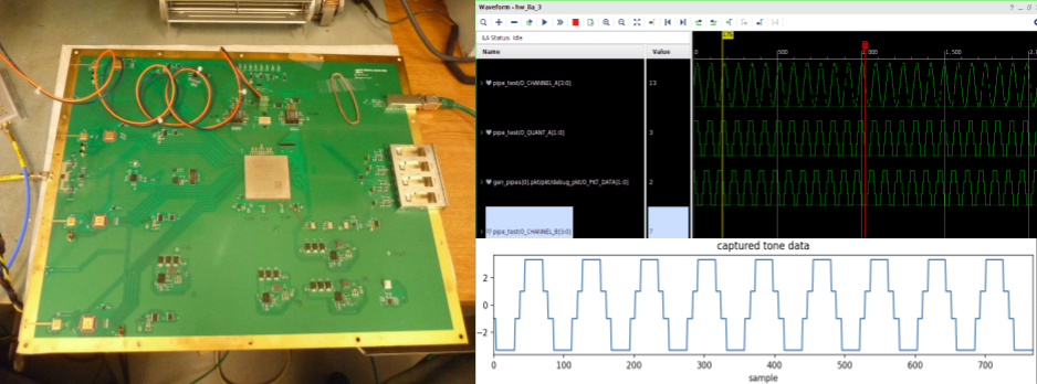
The platform for firmware development is the prototype ngDBE system, which uses a quad custom sampler PCB board interfaced via an FMC+ (Vita 57.4) connector to an evaluation board. The VCU128 is an AMD (formerly Xilinx) evaluation board hosting the VU37P, an FPGA which includes 8GB of high bandwidth memory (HBM). In this and alos in terms of logic fabric resources this chip is more powerful than needed. A custom production integrated board containing both four ADCs and the VU13P was chosen for the final design to improve reliability and robustness. The left panel of Figure 4 shows the first revision of the integrated custom board.
Using the evaluation platform, the core functionality of the firmware has been completed and tested. The fully designed and tested FPGA logic includes the following functional components:
-
•
ADC interface module
-
•
requantization block from 4-bits to 2-bits
-
•
packetization module
-
•
100 Gb/s Ethernet transmission module
-
•
Universal Asynchronous Receiver Transmitter (UART)
-
•
timing module
-
•
monitor and control module
Additional firmware features still under development for the ngDBE include polyphase filterbank (PFB) channelization, digital slope and ripple equalization, and 1 Gb/s Ethernet monitor and control. The PFB and equalization features are most likely descoped from the BHEX DBE in the interests of simplicity and reduced power consumption.
The functional verification of the ngDBE firmware uses Internal Logic Analyzers (ILA) instantiated on the FPGA to look at snippets of digitized, requantized and packetized data and a recording packet capture device that ingested the output from the DBE at half rate and the data was subsequently analyzed. The integrity of a sine wave input was verified. Correlation of noise like input data generated by an antenna emulator was also successfully performed using collected data from two of the four channels. The right panel of Figure 4 depicts the tone verification both on the ILA and from post-processing of data captured by the external hard drive.
4 BHEX Back End Electronics
The terrestrial progenitor systems discussed in section 3 verify functional performance and provide firmware readily adaptable to the BHEX system. Howeevr the hardware is not designed for flight in respect to radiation tolerance, vibration and thermal cooling in vacuum, size, weight, and power consumption—commonly referred to as “SWaP” for space payloads. The functional demonstration of a terrestrial system brings the back end, approximately, to Technology Readiness Level 4 (TRL-4). Using a terrestrial progenitor as an example, the R2DBE consumes 75 W, is housed in a box, and uses key components (ADCs and FPGAs) that do not have corresponding space qualified versions. Conversely, we aim to process the full BHEX data rate on a single, lower power digital back end (DBE) circuit board that is space qualified.
A Nyquist-sampled version of the received electric field in each band and both polarizations corresponds to an aggregate data rate of 64 gigabits-per-second (Gb/s), a formidably high data rate stream to downlink from a MEO orbit to earth. No data compression on orbit is possible because the digitized signal is random noise, most of which is introduced by the receiving system, with the faint black hole emission representing only one part in 100,000 of the total power.
VLBI detections involve cross-correlating across the “baselines” which connect stations—the difficult case being BHEX to any terrestrial station—followed by typically several minutes of integration. A correlation peak shows that the cosmic signal from the black hole has been detected at both stations given that the receiver noise is uncorrelated. The cross-correlation and attendant data reduction can only be done by a processor which has access to the signal from both stations. Thus correlation cannot be done on orbit prior to downlink. BHEX therefore requires a space-ready signal processing and transmission system that can transform the wideband analog signal to a very high rate digital data stream passing it to the optical downlink subsystem [1] which transmits the data payload to a ground station.
4.1 Trade Studies
This section describes selected examples of key design trades. Space qualified candidate components include three space qualified 10 GS/s ADC. The AMD/Xilinx Versal FPGA is available as a space qualified part in some variants. Given our data rates and need for fast and late generation SERDES, combined with the need for lower power, this device based on 7 nm finFET process is a clear choice. We are considering a “System in Package” (SiP) device from Mercury Systems, which uses the Versal, however this device is under Non Disclosure Agreement (NDA) and is not further described. The possibility of using a turnkey SiP is attractive, though has cumbersome aspects including the need for NDAs, and lack of clarity and process in respect of space qualification. The Mercury SiP highlighted a possible fourth ADC candidate from Jariet, though this option is also encumbered by NDA. An NDA is not yet in place, and so far we have not studied it.
4.1.1 Component Trade Example: ADC Selection
In this trade study three space qualified ADC candidates not under NDA are considered. All have maximum conversion rates 10 GS/s. The devices are Teledyne/e2v (EV10AS940), Analog Devices (AD9213S), and Texas Instruments (TI TI-ADC12DJ5200-SP), and their characteristics are summarized in table 1. All have substantial bit depth between 8 and 10 bits. They vary in total power consumption and analog input bandwidth. The Teledyne device having both the lowest power consumption and by far the widest analog input bandwidth of 33 GHz. The wide analog input bandwidth eliminates the need for a heterodyne stage (mixers, local oscillator, amplifiers) prior to the ADC, which is an attractive simplification of the analog preconditioning.
However the TI ADC provides the ability to reduce the number of lanes to four while still providing a viable and robust asynchronous JESD interface between the ADC and the FPGA. The FPGA power consumption is driven by the number of instantiated SERDES subsystems on the FPGA. Further, for an ADC requiring as many lanes as bits, the number of SERDES required for ADC interfacing alone, combined with the need for additional SERDES to implement fast Ethernet output drives to a multiple FPGA solution for the DBE alone. With yet another FPGA for the optical downlink subsystem, the configuration is non-optimal in terms of power consumption, complexity, and reliability.
Minimizing required SERDES therefore reduction of the number of FPGAs to a single unit to outweighs the need for a heterodyne mixer stage as part of the analog conditioning. On this basis the TI-ADC12DJ5200-SP has been provisionally selected, and the BHEX back end presented in this paper incorporates this device specifications in the design for the back end. There are other devices still under consideration, including the SiP product mentioned earlier from Mercury Systems and the Jariet ADC. Selection of one of these is still possible, and would then most likely be driven by considerations of simplifying some aspect of the processing elements or significant power savings.
| manuf. | device | analog bw | power | # bits | # lanes |
|---|---|---|---|---|---|
| Teledyne e2v | EV10AS940 | 33 GHz | 2.5 W | 10 | 11 |
| Analog Dev. | AD9213S | 6.5 GHz | 4.6 W | 8 | 8 |
| Texas Inst. | TI-ADC12DJ5200-SP | 8 GHz | 4 W | 8 | 4 |
4.1.2 FPGA Count - Development Complexity Trade
By reducing the required number of SERDES needed, the TI ADC enables a single FPGA solution for the DBE. Even more, there is then potential to share the FPGA between the DBE and optical downlink subsystem. Here the primary trade is related to the reduced component count, and consequently lower power and improved reliability, of the single FPGA solution. This is traded against the relative complexity of providing appropriate interface specifications between different firmware functions, developed by different teams, and with different legacy code-bases, within a single FPGA. These logic units use different clock rates requiring multiple clock domains within a single FPGA.
Layered on to this are the institutional aspects of coordinating code development between Smithsonian Astrophysical Observatory (SAO) and Lincoln Laboratories (LL), including differing repository systems, and limitations on information sharing. In the end, given SAO and LL are neighbors, and noting the need for close working relationships, the significant benefits of the single FPGA solution outweigh these concerns.
4.2 Requirements and Interface Specifications
Following system engineering formalism considerable effort has been expended to finalize level 4 (L4), level 5 (L5) requirements, and Interface Control Documents (ICD) for the back end. The L4 requirements focus on top level back end specifications as dictated by the science traceability matrix (STM)[2].
The L4 requirements include sampler bandwidths, power and bandpass requirements for the analog signal before digitization, data throughput rates from the back end, data formats which are interoperable with the ground stations, and mechanical, electrical and environmental specifications. The L5 requirements are component level specifications for the individual sub-components of the back end that derive from the L4 requirements themselves. They include hardware specifications for the converters, the FPGA, and additionally several requirements for the firmware.
4.3 Signal Layout
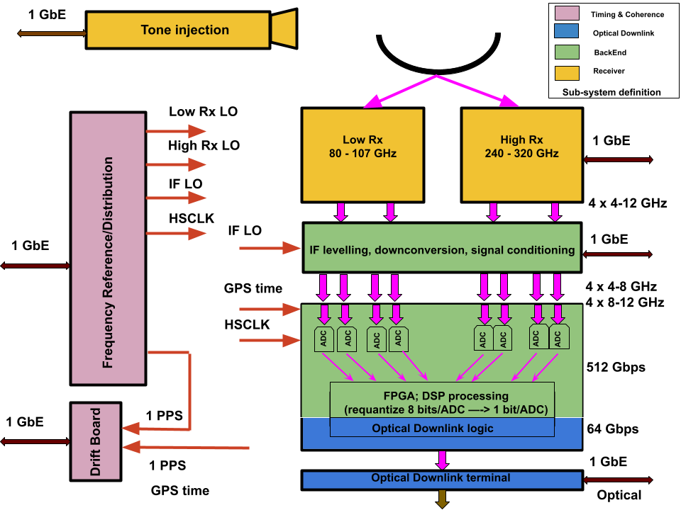
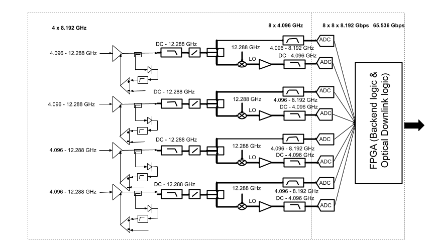
The cryogenic receivers operating at 1mm and 3mm output 4 IFs, each approximately 8 GHz wide which are DSB and single sideband respectively and dual polarization from 4-12 GHz. The reception and generation of the signals propagating through the entire instrument signal chain and the back end electronics is shown in the block diagram, Figure 5. A more detailed schematic of the back end electronics sub-system is shown in Figure 6. This preliminary design is the most feasible option at this point given considerations of requirements, performance, cost and space qualification. We expect it to undergo small revisions as the design matures, however we do not expect any substantial changes.
Using round numbers for convenience where appropriate, the lower sub-band is referred to as 4-8 GHz, the upper sub-band as 8-12 GHz, the total IF range as 4-12 GHz, and the instantaneous full single receive band as 8 GHz. Where needed these are expanding to the exact frequencies documented in figure 6.
4.4 BHEX BDC
The BHEX analog signal processing system includes a heterodyne system that performs a frequency translation from IF to baseband for parts of the band, and conditions it for digitization. The DBE is a fast digitizer sampling at 8.192 Gigasamples per second (Gsps), interfaced to digital logic implemented on a Field Programmable Gate Array (FPGA). 1-bit data output rates for each 16 GHz band with Nyquist sampling corresponds to 32 Gbps for a single frequency, or 64 Gbps for two simultaneous bands.
The analog signal processing stage breaks up the 8 GHz IF into two equally wide 4 GHz wide sub-bands for digitization by the subsequent stage and conditions it. The very first stage in this signal chain is the Automatic Gain Control (AGC) section which levels the amplitude to a predetermined value to keep the downstream signal chain unaffected by receiver output power variations. A Nyquist prefilter prevents aliasing, and slope equalization corrects for gain variations across the passband These features are implemented for all IF outputs following the AGC. Two sub-bands are generated from the contiguous IF of 4-12 GHz using band pass and low pass filters. The 4-8 GHz sub-band can be direct RF sampled. The 8-12 GHz cannot be direct RF sampled and is therefore downconverted to DC-4 GHz. The depicted configuration also introduces a spectral inversion. The mixing process causes requiring the addition of a gain to the heterodyne system.
4.5 BHEX DBE
The conditioned sub-bands are digitized by eight analog to digital converters which are sampled at 8.192 Gsps. This specific number derives from an inter-operability requirement with the EHT array. The native resolution of the TI ADC is 12-bits, however it is configurable to sample with 8-bits which is more than adequate for our purposes. The 4-8 GHz sub-band is direct RF sampled in the second Nyquist zone of the sampler. The 8-12 GHz sub-band which is now the downconverted DC-4 GHz sub-band is sampled in the first Nyquist zone. The proposed analog to digital converter for BHEx has been identified after a component trade study as described in section 4.1.1. This has been determined to be the most optimal converter in terms of a combination of interrelated factors, including conversion rate, input bandwidth, high-rate data transfer options, power dissipation, and availability in a spaceflight version (radiation hardness, hermetic package, etc.). The trade studies for ADC’s also included pushing the State of the Art, by including newly-developed microcircuits.
4.6 FPGA Digital Signal Processing (DSP)
The digitized data from all the samplers are routed to an AMD Versal AI core VC1902 FPGA which is the most suitable FPGA for this application. A trade study to finalize the choice of the critical FPGA of the back end. As with the choice of converters, this FPGA is available in a spaceflight version which makes it eminently suitable. The The FPGA firmware consists of the following primary digital signal processing modules as listed and described below:
-
1.
The converter interfaces with the FPGA using a standardized multigigabit serial data standard called JESD204. This protocol is developing as the interface of choice with the selected converter employing the third revision of the protocol named JESD204C.
-
2.
The 8-bit data is re-quantized down to 1 bit to reduce the data rates from a staggering 512 Gbps to a manageable 64 Gbps.
-
3.
The data are converted into UDP packets and relevant header information is attached to the packets in the standard VDIF format which is an EHT requirement.
-
4.
The UDP packets are handed off to the next sub-system over the predetermined interface.
The ngDBE FPGA firmware described in section 3.4 has been developed to an advanced level and has many of the features required by the above BHEX firmware. Porting from the Ultrascale+ FPGA used in ngDBE to the Versal FPGA used in BHEX is expected to be fairly straightforward with some adaptations to hardware environment needed. It is likely that BHEX will use a stripped down feature set. For example BHEX will only transmit one bit samples to reduce the size of data payloads on the optical downlink. Other simplifications aim to reduce firmware complexity and FPGA power consumption. Simplifications under consideration include the elimination of polyphase filter bank (PFB) channelization and digital equalization, though the final decision on these trades is expected to be made with consideration of quantitative estimates or measurements of the actual power consumption and attendant savings.
4.7 Buffer Memory
With the 16 GB as a placeholder, installing smaller, or even larger DRAM doesn’t have to change the site or package size. System considerations including the number of terrestrial optical downlink terminals and a tolerable bit error level may mean that no no buffer at all is needed. The buffer memory site on the “terrestrial equivalent” TRL advancement hardware might then later be eliminated in a flight qualified version.
“High Bandwidth Memory” (HBM) is an on-chip option on modern FPGAs, available in Ultrascale+ and Versal, and can have substantial depth. Certainly there are 8 GB versions available. However HBM is not an option in flight qualified Versal FPGAs. So there is no possibility to provide the buffer on-FPGA, and therefore the buffer size is not going to drive the 1 vs. 2 FPGA decision. Combining the DBE and downlink Versal and firmware is a likely outcome.
4.8 Power Estimation
The known power consumption of the ngDBE firmware is a conservative active power estimate. Given the improved smaller feature size FinFET technology of Versal relative to Ultrascale+ (7 nm and 16 nm respectively) such an estimate is sure to be conservative. DBE power is a relatively small contributor to overall mission power requirements—compared to cryogenics, for example—so small variations in our estimate are of little consequence.
5 Summary and Path Forward
This paper has described the BHEX system in the context of existing terrestrial VLBI systems, and pre-design studies of the BHEX system requirements and component options. Following system engineering process, requirements tables and interface specifications to upstream and downstream systems have been developed. Top level design of the electronics hardware is described with top level, logic, and schematic diagrams. Selection trade studies for main component parts are nearing completion, and have identified analog-to-digital converters from Texas Instruments, and the preferred FPGA in the Versal family from AMD.
The next stage is detailed design and construction of a TRL-advancement prototype of the BHEX BDC and DBE using terrestrial grade parts which are available in functionally identical space grade equivalents. Existing FPGA firmware developed for the terrestrial ngDBE will be adapted for BHEX and tested for fault tolerance. Testing of the terrestrial equivalent prototype with other subsystem elements—receiver upstream, optical downlink downstream, and under coherent frequency reference discipline—aims to verify functionality. Combining careful selection of parts available in space grade versions with planned environmental testing at the University of Arizona in late 2024 aims to retire risk and further advance the BHEX back end TRL. The objective is to prepare for a Small Explorer (SMEX) mission proposal in 2025.
Acknowledgements.
Technical and concept studies for BHEX have been supported by the Smithsonian Astrophysical Observatory, by the Internal Research and Development (IRAD) program at NASA Goddard Space Flight Center, and by the University of Arizona. We acknowledge financial support from the Brinson Foundation, the Gordon and Betty Moore Foundation (GBMF-10423), the National Science Foundation (AST-2307887, AST-1935980, and AST-2034306). This project/publication is funded in part by the Gordon and Betty Moore Foundation (Grant #8273.01). It was also made possible through the support of a grant from the John Templeton Foundation (Grant #62286). The opinions expressed in this publication are those of the author(s) and do not necessarily reflect the views of these Foundations. BHEX is funded in part by generous support from Mr. Michael Tuteur and Amy Tuteur, MD. BHEX is supported by initial funding from Fred Ehrsam.References
- [1] Wang, J., Boroson, D., Schieler, C., Bilyeu, B., Shtyrkova, K., Caplan, D., Johnson, M., Weintraub, J., Srinivasan, R., Haworth, K., Houston, J., Blackburn, L., Richards, E., and Marrone, D. P., “High rate laser communications for the black hole explorer,” Submitted to the SPIE Conference Series (May 2024).
- [2] Johnson, M. D., Akiyama, K., Baturin, R., Bilyeu, B., Blackburn, L., Boroson, D., Cárdenas-Avendaño, A., Chael, A., Chang, D., Chan, C.-k., Cheimets, P., Chou, C., Doeleman, S. S., Farah, J., Galison, P., Gamble, R., Gammie, C. F., Gelles, Z., Gómez, J. L., Gralla, S. E., Grimes, P., Gurvits, L. I., Hadar, S., Haworth, K., Hada, K., Hecht, M. H., Honma, M., Houston, J., Hudson, B., Issaoun, S., Jia, H., Jorstad, S., Kauffmann, J., Kovalev, Y. Y., Kurczynski, P., Lafon, R., Lupsasca, A., Lehmensiek, R., Ma, C.-P., Marrone, D. P., Marscher, A. P., Melnick, G., Narayan, R., Niinuma, K., Noble, S. C., Palmer, E. J., Palumbo, D., Paritsky, L., Peretz, E., Pesce, D., Petrov, L., Plavin, A., Quataert, E., Rana, H., Ricarte, A., Roelofs, F., Shtyrkova, K., Sinclair, L. C., Small, J., Tirupati Kumara, S., Srinivasan, R., Strominger, A., Tiede, P., Tong, E., Wang, J., Weintroub, J., Wielgus, M., Wong, G., and Zhang, X. A., “The black hole explorer: Motivation and vision,” Submitted to the SPIE Conference Series (May 2024).
- [3] Event Horizon Telescope Collaboration, “First M87 Event Horizon Telescope Results. I. The Shadow of the Supermassive Black Hole,” ApJ 875, L1 (Apr 2019).
- [4] Event Horizon Telescope Collaboration, “First Sagittarius A* Event Horizon Telescope Results. I. The Shadow of the Supermassive Black Hole in the Center of the Milky Way,” ApJ 930, L12 (may 2022).
- [5] Tong, E. C., Akiyama, K., Grimes, P., Honma, M., Houston, J., Johnson, M., Marrone, D. P., Rana, H., and Uzawa, Y., “Receivers for The Black Hole Explorer (BHEX) mission,” Submitted to the SPIE Conference Series (May 2024).
- [6] Wang, J. P., Bilyeu, B., Boroson, D., Caplan, D., Robinson, B., Schieler, C., Johnson, M., Blackburn, L., Doeleman, S., and Haworth, K., “High-rate 256+ Gbit/s laser communications for enhanced high-resolution imaging using space-based very long baseline interferometry (VLBI),” in [Society of Photo-Optical Instrumentation Engineers (SPIE) Conference Series ], Hemmati, H. and Robinson, B. S., eds., Society of Photo-Optical Instrumentation Engineers (SPIE) Conference Series 12413, 1241308 (Mar. 2023).
- [7] Srinivasan, R., Richards, E., Weintroub, J., Test, J., Freeman, M., Haworth, K., Johnson, M., Cheimets, P., Houston, J., Wang, J., Bilyeu, B., Fernandez, M., Mamani, E., Pola, A. L., Gendelman, M., and Marrone, D. P., “The black hole explorer back-end electronics,” Submitted to the SPIE Conference Series (May 2024).
- [8] Akiyama, K., Niinuma, K., Hada, K., Doi, A., Hagiwara, Y., Higuchi, A. E., Honma, M., Kawashima, T., Kolev, D., Koyama, S., Masui, S., Ohsuga, K., Sano, H., Takami, H., Tsunetoe, Y., Uzawa, Y., Akahori, T., Akiyama, Y., Galison, P., Hayashi, T. J., Hirota, T., Inoue, M., Iwata, Y., Johnson, M. D., Kino, M., Kofuji, Y., Mizuno, Y., Moriyama, K., Nagai, H., Nakamura, K., Notsu, S., Ono, F., Oya, Y., Oyama, T., Rana, H., Saida, H., Saito, R., Saito, Y., Sasada, M., Sawada-Satoh, S., Takahashi, M. M., Takamura, M., Tong, E., Tsuji, H., Yoshioka, S., and Watanabe, Y., “The japanese vision for the black hole explorer mission,” Submitted to the SPIE Conference Series (May 2024).
- [9] Marrone, D. P., Houston, J., Akiyama, K., Bilyeu, B., Boroson, D., Grimes, P., Haworth, K., Lehmensiek, R., Peretz, E., Rana, H., Sinclair, L. C., Sridharan, T. K., Srinivasan, R., Tong, E., Wang, J., Weintroub, J., and Johnson, M. D., “The black hole explorer: Instrument system overview,” Submitted to the SPIE Conference Series (May 2024).
- [10] Peretz, E., Kurczynski, P., Johnson, M., Houston, J., Sridharan, T. K., Wang, J., Galison, P., Gamble, R., Marrone, D. P., Noble, S., Melnick, G., Petrov, L., Rana, H., Haworth, K., Doeleman, S. S., Issaoun, S., Hadar, S., Lupsasca, A., Tong, E., Akiyama, K., Srinivasan, R., Boroson, D., Yang, G., Hoerbelt, T., Small, J., Honma, M., Bilyeu, B., Canavan, E., Shtyrkova, K., Lafon, R., Paritsky, L., Sinclair, L. C., Silver, M., Gurvits, L. I., Kovalev, Y., and Lehmensiek, R., “The black hole explorer: Astrophysics mission concept engineering study report,” Submitted to the SPIE Conference Series (May 2024).
- [11] Lupsasca, A., Cárdenas-Avendaño, A., Palumbo, D. C., and Johnson, M. D., “The black hole explorer: Photon ring detection and shape measurement,” Submitted to the SPIE Conference Series (May 2024).
- [12] Galison, P., Lupsasca, A., and Johnson, M., “The black hole explorer: Using the photon ring to visualize spacetime around the black hole,” Submitted to the SPIE Conference Series (May 2024).
- [13] Issaoun, S., Akiyama, K., Alonso, K., Blackburn, L., Boroson, D., Galison, P., Haworth, K., Houston, J., Johnson, M. D., Kovalev, Y. Y., Kurczynski, P., Lafon, R., Marrone, D. P., Palumbo, D., Peretz, E., Pesce, D., Petrov, L., Plavin, A., and Wang, J., “The black hole explorer: Operating a hybrid observatory,” Submitted to the SPIE Conference Series (May 2024).
- [14] Kawashima, T., Tsunetoe, Y., and Ohsuga, K., “Black hole spacetime and properties of accretion flows and jets probed by black hole explorer,” Submitted to the SPIE Conference Series (May 2024).
- [15] Tomio, H., Numata, K., Yang, G., Attar, A., Lu, W., Xu, X., Leopardi, H. F., Gramling, C., Sridharan, T. K., and Kurczynski, P., “Ultra-low noise laser and optical frequency comb-based timing system for the black hole explorer (bhex) mission,” Submitted to the SPIE Conference Series (May 2024).
- [16] Sridharan, T. K., Lehmensiek, R., Cheimets, P., Freeman, M., Houston, J., Johnson, M., Marrone, D. P., and Silver, M., “The black hole explorer (bhex): Preliminary antenna design,” Submitted to the SPIE Conference Series (May 2024).
- [17] Rana, H., Akiyama, K., Canavan, E. R., DiPirro, M. J., Freeman, M., Galison, P., Grimes, P. K., Hada, K., Honma, M., Houston, J., Johnson, M., Kimball, M. O., Marrone, D. P., Niinuma, K., and Tong, E., “The black hole explorer (bhex) cryocooling instrument,” Submitted to the SPIE Conference Series (May 2024).
- [18] Vertatschitsch, L., Primiani, R., Young, A., Weintroub, J., Crew, G. B., McWhirter, S. R., Beaudoin, C., Doeleman, S., and Blackburn, L., “R2DBE: A Wideband Digital Backend for the Event Horizon Telescope,” PASP 127, 1226 (Dec. 2015).
- [19] Primiani, R. A., Young, K. H., Young, A., Patel, N., Wilson, R. W., Vertatschitsch, L., Chitwood, B. B., Srinivasan, R., MacMahon, D., and Weintroub, J., “SWARM: A 32 GHz Correlator and VLBI Beamformer for the Submillimeter Array,” Journal of Astronomical Instrumentation 5, 1641006–810 (Dec. 2016).
- [20] Doeleman, S. S., Barrett, J., Blackburn, L., Bouman, K. L., Broderick, A. E., Chaves, R., Fish, V. L., Fitzpatrick, G., Freeman, M., Fuentes, A., Gómez, J. L., Haworth, K., Houston, J., Issaoun, S., Johnson, M. D., Kettenis, M., Loinard, L., Nagar, N., Narayanan, G., Oppenheimer, A., Palumbo, D. C. M., Patel, N., Pesce, D. W., Raymond, A. W., Roelofs, F., Srinivasan, R., Tiede, P., Weintroub, J., and Wielgus, M., “Reference Array and Design Consideration for the Next-Generation Event Horizon Telescope,” Galaxies 11, 107 (Oct. 2023).
- [21] Event Horizon Telescope Collaboration, “First M87 Event Horizon Telescope Results. VII. Polarization of the Ring,” ApJ 910, L12 (Mar. 2021).