Substratebias driven Sputter deposited phase dominated Tungsten film for Spintronic applications
Abstract
-Tungsten (-W), a A15 cubic phase of Tungsten exhibits giant spin hall angle as compared to its bcc-phase -Tungsten (-W), making high quality -W film desirable for spin-based application. We report on the substrate bias driven on-demand growth of -W film on SiO2 coated silicon (SiO2/Si) using DC sputtering. GIXRD plots and SEM images are used to show a systematic change on the structure and grain size of the deposited films with the application of substrate bias. It is observed that zero bias film are amorphous in nature and changes phase from to or mixed ( + ) depending upon the sign and magnitude of the substrate bias. We performed One-Dimensional Power spectrum density of the AFM images which revealed that the pure -W film grown at a positive bias of +50V has the minimum roughness as compared to films grown at different substrate bias. We further confirm the metallic surface homogeneity using the room temperature STM. Our results shows that the substrate bias which controls the energy of the deposited atom, is a crucial parameter for an on demand growth of -W, an important material for spintronic applications.
Heavy metal (HM) thinfilms are critical building blocks in spintronics technology, providing the means for efficient spin manipulation and transport, which are essential for the development of next-generation electronic and computing devicesPeng et al. (2019); Ramaswamy et al. (2018). Owing to the large spin-orbit coupling, HM are efficient in converting charge current into spin currentHirsch (1999); Li et al. (2005). Moreover in heterostructure with magnetic layer, HM leads to generation of spin-orbit torques for magnetic switching as well as induces interfacial Dzyaloshinskii-Moriya interaction (DMI) that stabilizes exotic spin textures such as chiral domain walls as well as Skyrmions in magnetic layersZhu et al. (2019); Li et al. (2016); Miron et al. (2011); Torrejon et al. (2014); Ma et al. (2016). Heavy metals like platinum (Pt), tungsten (W), palladium (Pd), and others have been extensively studied over the last few decades to understand their functionalities and potential applications in spintronicsWoo et al. (2014); Hao et al. (2015); Pai et al. (2012); Vudya Sethu et al. (2021); Jamali et al. (2013); Liu et al. (2012).
Tungsten can exist in two major forms: -tungsten (-W), which has a body-centered cubic (BCC) crystal structure, and -tungsten which is characterized by an A15 crystal structure and exhibits higher resistivity as compared to -WWeerasekera et al. (1994); Lee et al. (2016); Petroff et al. (1973). Tungsten, as a heavy metal, has indeed attracted significant attention in spintronic research owing to the giant spin Hall effect observed in its metastable phase knows as -tungsten (-W)Hao et al. (2015); Pai et al. (2012); Demasius et al. (2016). Despite its potential, achieving a pure -phase thinfilm proves challenging, and the precise factors leading to the formation of the -phase remain unclear. Prior studies have attributed the formation of -phase to the incorporation of oxygen impurities during growthWeerasekera et al. (1994); Shen and Mai (2000); Chattaraj et al. (2020). Moreover, it is also argued that the phase transition from to phase happens around a critical thickness close to the spin diffusion length in tungstenHao et al. (2015); Pai et al. (2012); Choi (2017); Rossnagel et al. (2002).
In this work, we report on achieving controlled phase transition from to -W in films with thicknesses much larger than the spin diffusion length using substrate bias during DC sputtering. The phases of the deposited films were confirmed based on X-ray diffraction and resistivity measurement. The surface morphology studied using AFM, SEM and STM clearly demonstrate the influence of DC bias on the nucleation and growth kinetics of tungsten grains on the substrate surface. The films evolve from an amorphous cauliflower like structure at zero bias condition to more structured grains with the application of positive or negative bias to the substrate.
A series of tungsten films were grown using DC magnetron sputtering on SiO2 coated silicon (Si/SiO2) substrates. The silicon substrates (Si/SiO2) underwent a cleaning process involving ultrasonication for 10 minutes in acetone, isopropyl alcohol (IPA), and DI water, respectively followed by drying with nitrogen gas before being mounted on an electrical-floated substrate holder in the vacuum chamber. A 2-inch cathode target of Tungsten (99.95% purity), procured from Testbourne, UK, was maintained at a distance of 10cm from the substrate holder. The base pressure for the deposition was torr. For sputtering we obtain plasma with a Ar gas flowrate of 18 standard cubic centimetres per minute (sccm) controlled by a mass flow controller (MFC) maintaining a working pressure of 1 mTorr. Before starting the deposition, the W target was pre-sputtered for 5 mins to remove contamination from the target surface. The sputtering time was 30 mins. All films were deposited under similar condition except the applied substrate bias voltage, which was systematically varied from -100 V to +100 V. Thus, we have a set of 5 tungsten film deposited at substrate bias of : -100 V, -50 V, 0 V, +50 V, and +100 V.
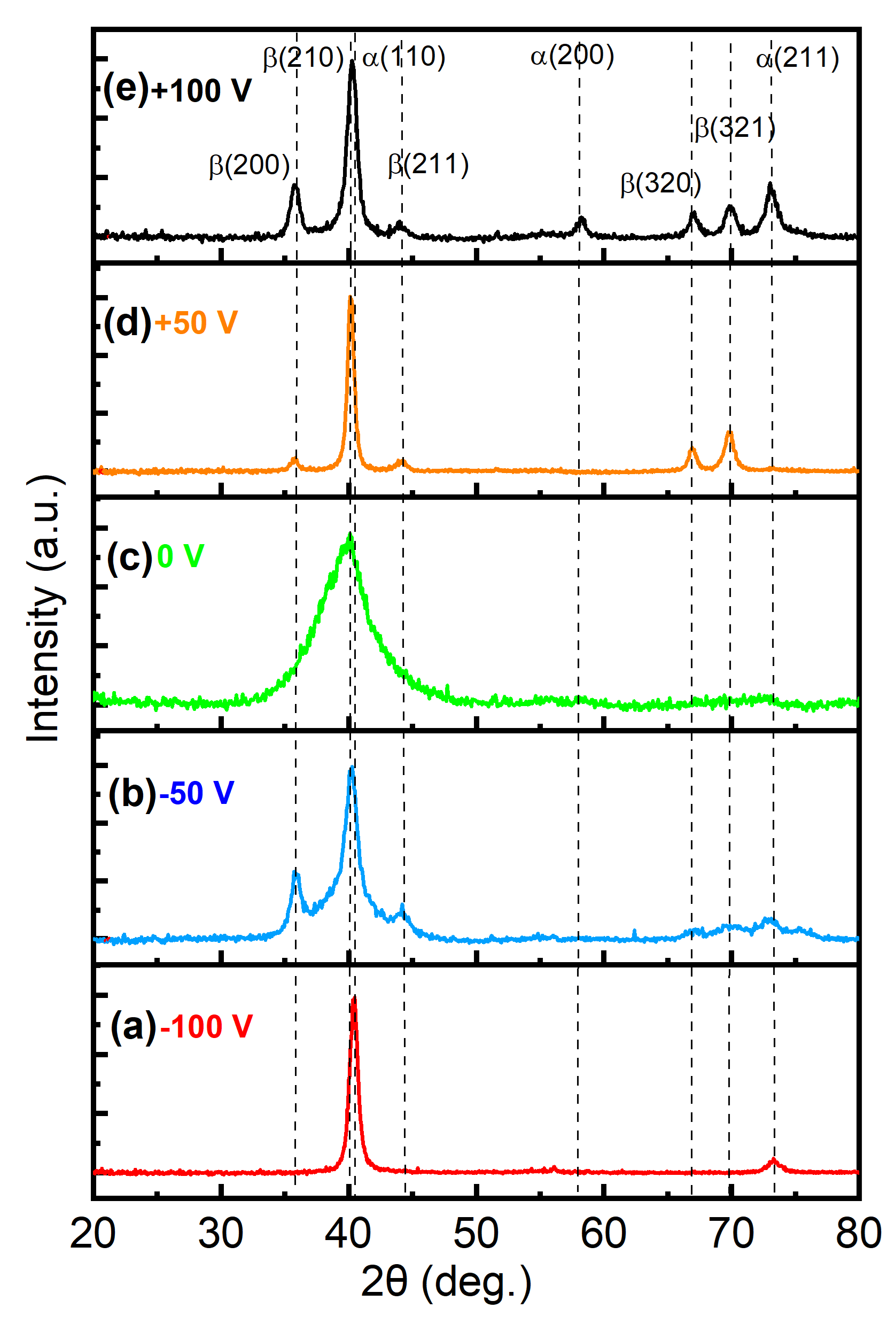
The crystal structure of the as-grown films of W under different substrate bias condition was studied using X-ray diffraction. Figure 1 shows the Grazing Incidence X-ray Diffraction (GIXRD) data within the 2 range of 20∘ to 80∘ acquired utilizing Cu K- radiation ( = 1.54Å). At zero-bias (Fig.1(c)) a broad peak is observed around 2 = 40∘ which indicates the amorphous nature of the deposited film. As the negative bias of -50V is applied during growth (Fig.1(b)), we observe a semi-crystalline film where the broad peak at 2 = 40∘ starts to resolve into fine structures as well as some additional broad peaks appear around 2 = 70∘. However, these peak position confirms that the grown film at -50V bias has a mixed phase of and -W. Further increasing the negative bias voltage to -100V (Fig.1(a)), we observe sharp GIXRD peaks highlighting the crystalline nature of the film with peak position matching the pure -W and showing preferential orientation along -(110)Petroff et al. (1973); Ahn et al. (2023). Based on the peak position we obtain a lattice constant of 3.155 ÅWeerasekera et al. (1994). Now, with positive bias of +50V (Fig.1(d)), a crystalline film is formed with the peak position matching the pure -W phase with a lattice constant of 5.084 ÅWeerasekera et al. (1994); Petroff et al. (1973); Ahn et al. (2023). This demonstrate a controlled growth of -W film in an oxygen-free atmosphere. As the bias voltage is increased to +100V (Fig.1(e)), the film is crystalline but shows a mixed phase of and -W. The GIXRD data demonstrate that the resulting phase of the tungsten film strongly depends on the substrate bias voltage. The substrate bias besides controlling the crystallinity, can also be used to tune the orientation of the deposited film as well as on-demand growth of pure -W film.
SEM images in Figure 2 shows the surface morphology of the deposited W film on Si/SiO2 substrate under different substrate bias condition. At zero (Fig.2(c)) as well as at -50V (Fig.2(b))bias voltage, cauliflower like structure is observed. With the increase of negative bias to -100V (Fig.2(a)), the morphology evolves into polyhedron grains of dimensions 100nm. For positive bias of +50V (Fig.2(d)), the uniform polyhedron grains of dimensions 40nm is observed. However, the films deposited at +100V (Fig.2(e)) exhibited needle like structure characterised by grain sizes of nearly 100nm. Thus, the tungsten film with the pure phase (+50V) has the smallest grain sizeLee et al. (2016).
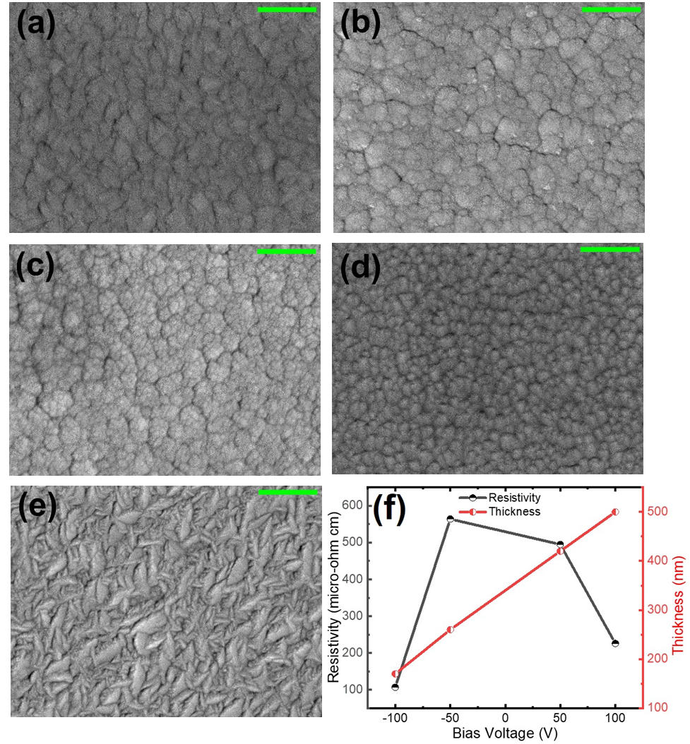
Previous electron transport properties has established that phase of W has lower resistivity as compared to pure phasePetroff et al. (1973). Figure 2(f) shows the resistivity of the deposited films in this study measured using Four-probe method. The film grown at -100V has the lowest resistivity of around 100-cm owing to the larger grain size and pure phase observed for this filmAhn et al. (2023). At the substrate bias of +50V, the film has higher resistivity of around 500-cm which can be explained due to the pure phase as well as smaller grain size that increases the overall scattering of electronsPetroff et al. (1973); Ahn et al. (2023). For the film grown at -50V (570-cm) as well as at zero bias (1200-cm(not shown in the Fig.2(f))), the resistivity is found to be higher than the phase due to the semi-crystalline and/or amorphous nature of these film as confirmed from XRD. Finally, the +100V film has lower resistivity as compared to the film grown at +50V due the larger grain size as well as the mixed and -W phase observed in this film.
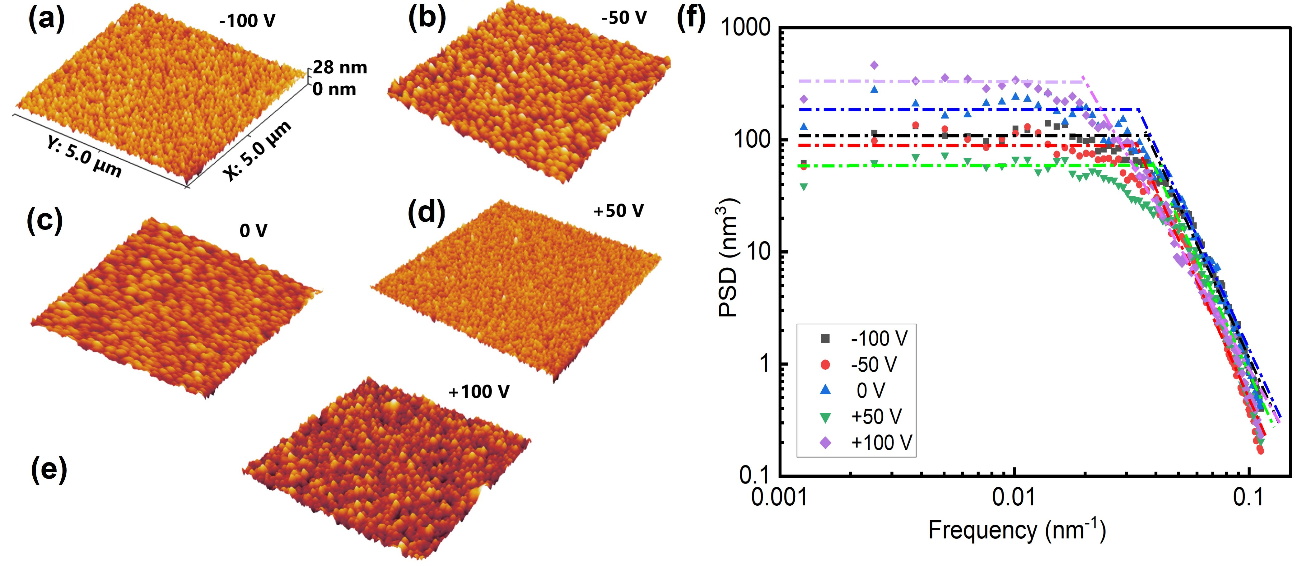
Thus we have shown that substrate bias can be used to grow desirable phase of W films important for the spintronic application. Beside the phase, the surface roughness of the HM plays crucial role for defining interfacial properties essential for spin Hall Effect or spin orbit torque based applicationsHait et al. (2022); Fan et al. (2014). To analyse the effect of substrate bias on the roughness of the grown film, we performed power spectral density (PSD) analysis of the AFM data. Figure 3 shows the AFM data with scanning range of 5m 5m for films grown with different substrate bias. Thinfilm grown by sputtering are generally self-affine surfaces exhibiting statistical scaling properties over different length scales, and PSD analysis helps quantify these properties. PSD is evaluated from the Fourier transform of the autocorrelation function of power signals across wide spatial frequency range. In this paper, one dimensional approach has been adopted for the computation of PSD function, which follows the equationBabich et al. (2022)
| (1) |
where is the spatial frequency and is the Fourier coefficient of the line profile defined as:
| (2) |
and are the number of points in a profile and number of profiles, respectively. is a pixel dimension along the line, and is the value of the height at the point in the line-profile.
Figure 3(f) represents the log-log plot of the 1D-PSD profile as a function of spatial frequency for different AFM images shown in Fig.3. All 1D-PSD profiles represents a typical self-affine surface characterised by a low frequency plateau and a linearly varying high frequency regionWang et al. (2019). The intensity of the plateau region corresponds to the roughness associated the transition point between plateau and linearly varying region also called the inflection point represents the inverse of the correlation lengthBabich et al. (2022); Eftekhari et al. (2022). PSD profile clearly shows that for the film grown with +50V substrate bias corresponding to the -phase of the film has the lowest intensity for the plateau region highlighting the minimum associated roughness. Table 1 shows the roughness obtained using k-correlation model and the corresponding correlation length obtained from knee point in the 1D-PSD profile. Lowest correlation length for the +50V voltage corresponds to the smallest grain size observed in the SEM images.
| DC bias voltage (V) | +100 | +50 | 0 | -50 | -100 |
| RMS roughness (nm) | 0.9 | 0.6 | 1.0 | 0.7 | 0.8 |
| Correlation length (nm) | 53 | 26 | 33 | 30 | 28 |
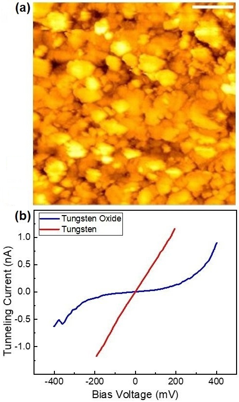
Finally, we further characterised the deposited film using Scanning Tunnelling Microscope (STM) to demonstrate the stable homogeneous metallic surface throughout the grown film. Figure 4(a) shows the STM image for a +50V deposited film obtained at ambient condition under constant current mode where a current of 0.2nA was maintained with an application of Tip-to-Sample voltage of -0.3V. See supplementary information for STM image for all other films grown at different bias condition. The constant current STM images gives topography matching the features seen in SEM or AFM. Typical Tunnelling current vs applied Tip-Sample voltage averaged over the scan area for a film grown at substrate bias of +50V is show as red-line in Fig.4(b). A linear behaviour of the Tunnelling current with the applied Tip-Sample voltage is a signature of chemically homogeneous surface with metallic electronic densityBesenbacher (1996). This further confirms the high quality of the deposited -W films using a positive substrate bias of +50V. The blue-curve in Figure 4(b) show a Tunnelling current vs voltage characteristic for a similar film grown at +50V but subsequently annealed in air at . After annealing the film is oxidised giving rise to a typical semiconducting I-V characteristic for Tungsten OxideSantucci et al. (2000). Thus STM I-V characteristics can be easily used to differentiate between homogeneous metallic phase or a partially oxidised surface containing oxide phase embedded in metallic matrix.
Thus we have demonstrated a controlled/on-demand sputter growth of -W with variation of substrate bias. The -phase is stable even for thick film (430nm) grown in this study in contrary to the previous report observing -phase only below a critical thickness of 22nm. Moreover, some previous study also claim that or phase of the tungsten film depends upon the incorporation of oxygen content during the deposition of the film. However, our results demonstrate that oxygen does not play a role in obtaining -phase as all the films were grown under similar condition except the variation in applied substrate bias. Substrate bias in sputtering plays a crucial role in controlling the energy of deposited atoms, thereby influencing the properties of the thin films produced. We claim that an optimum energy is needed for the growth of -phase which can be controlled with the application substrate bias if all other sputtering conditions remain unchanged. Further theoretical study is needed to understand the growth dynamics under the influence of substrate bias during sputter growth of Tungsten film.
Acknowledgement
This work was financially supported by Science and Engineering Research Board (SERB) Start-Up Research Grant (SRG/2021/002186) and University Grants Commission (UGC) Start-up research grant (F.30-569/2021).
Author Declaration
Conflict of Interest:The authors have no conflicts to disclose.
Data Availability
The data that support the findings of this study are available from the corresponding author upon reasonable request.
References
- Peng et al. (2019) S. Peng, D. Zhu, J. Zhou, B. Zhang, A. Cao, M. Wang, W. Cai, K. Cao, and W. Zhao, Advanced Electronic Materials 5, 1900134 (2019).
- Ramaswamy et al. (2018) R. Ramaswamy, J. M. Lee, K. Cai, and H. Yang, Applied Physics Reviews 5 (2018).
- Hirsch (1999) J. Hirsch, Physical review letters 83, 1834 (1999).
- Li et al. (2005) J. Li, L. Hu, and S.-Q. Shen, Physical Review B 71, 241305 (2005).
- Zhu et al. (2019) L. Zhu, D. Ralph, and R. Buhrman, Physical review letters 122, 077201 (2019).
- Li et al. (2016) P. Li, T. Liu, H. Chang, A. Kalitsov, W. Zhang, G. Csaba, W. Li, D. Richardson, A. DeMann, G. Rimal, et al., Nature communications 7, 12688 (2016).
- Miron et al. (2011) I. M. Miron, K. Garello, G. Gaudin, P.-J. Zermatten, M. V. Costache, S. Auffret, S. Bandiera, B. Rodmacq, A. Schuhl, and P. Gambardella, Nature 476, 189 (2011).
- Torrejon et al. (2014) J. Torrejon, J. Kim, J. Sinha, S. Mitani, M. Hayashi, M. Yamanouchi, and H. Ohno, Nature communications 5, 4655 (2014).
- Ma et al. (2016) X. Ma, G. Yu, X. Li, T. Wang, D. Wu, K. S. Olsson, Z. Chu, K. An, J. Q. Xiao, K. L. Wang, et al., Physical Review B 94, 180408 (2016).
- Woo et al. (2014) S. Woo, M. Mann, A. J. Tan, L. Caretta, and G. S. Beach, Applied Physics Letters 105 (2014).
- Hao et al. (2015) Q. Hao, W. Chen, and G. Xiao, Applied Physics Letters 106 (2015).
- Pai et al. (2012) C.-F. Pai, L. Liu, Y. Li, H. Tseng, D. Ralph, and R. Buhrman, Applied Physics Letters 101 (2012).
- Vudya Sethu et al. (2021) K. K. Vudya Sethu, S. Ghosh, S. Couet, J. Swerts, B. Sorée, J. De Boeck, G. S. Kar, and K. Garello, Physical Review Applied 16, 064009 (2021).
- Jamali et al. (2013) M. Jamali, K. Narayanapillai, X. Qiu, L. M. Loong, A. Manchon, and H. Yang, Physical review letters 111, 246602 (2013).
- Liu et al. (2012) L. Liu, C.-F. Pai, Y. Li, H. Tseng, D. Ralph, and R. Buhrman, Science 336, 555 (2012).
- Weerasekera et al. (1994) I. Weerasekera, S. I. Shah, D. V. Baxter, and K. Unruh, Applied Physics Letters 64, 3231 (1994).
- Lee et al. (2016) J.-S. Lee, J. Cho, and C.-Y. You, Journal of Vacuum Science & Technology A 34 (2016).
- Petroff et al. (1973) P. Petroff, T. Sheng, A. Sinha, G. Rozgonyi, and F. Alexander, Journal of Applied Physics 44, 2545 (1973).
- Demasius et al. (2016) K.-U. Demasius, T. Phung, W. Zhang, B. P. Hughes, S.-H. Yang, A. Kellock, W. Han, A. Pushp, and S. S. Parkin, Nature communications 7, 10644 (2016).
- Shen and Mai (2000) Y. Shen and Y. Mai, Materials Science and Engineering: A 284, 176 (2000).
- Chattaraj et al. (2020) A. Chattaraj, M. Balal, A. K. Yadav, S. R. Barman, A. K. Sinha, S. N. Jha, S. Joulie, V. Serin, A. Claverie, V. Kumar, et al., Scientific Reports 10, 14718 (2020).
- Choi (2017) D. Choi, Microelectronic Engineering 183, 19 (2017).
- Rossnagel et al. (2002) S. M. Rossnagel, I. C. Noyan, and C. Cabral Jr, Journal of Vacuum Science & Technology B: Microelectronics and Nanometer Structures Processing, Measurement, and Phenomena 20, 2047 (2002).
- Ahn et al. (2023) S. M. Ahn, G. S. Jang, D. Y. Kim, and N.-M. Hwang, Electronic Materials Letters 19, 298 (2023).
- Hait et al. (2022) S. Hait, S. Husain, V. Barwal, L. Pandey, N. Sharma, N. K. Gupta, N. Kumar, and S. Chaudhary, Surfaces and Interfaces 33, 102259 (2022).
- Fan et al. (2014) X. Fan, H. Celik, J. Wu, C. Ni, K.-J. Lee, V. O. Lorenz, and J. Q. Xiao, Nature communications 5, 3042 (2014).
- Babich et al. (2022) E. Babich, S. Scherbak, E. Lubyankina, V. Zhurikhina, and A. Lipovskii, Sensors 22, 593 (2022).
- Wang et al. (2019) X. Wang, R. Zang, J. Gao, C. Liu, L. Wang, W. Gong, X. Zha, X. Chen, F. Huang, K. Javaid, et al., Advanced Materials Interfaces 6, 1900031 (2019).
- Eftekhari et al. (2022) L. Eftekhari, D. Raoufi, M. J. Eshraghi, and M. Ghasemi, Semiconductor Science and Technology 37, 105011 (2022).
- Besenbacher (1996) F. Besenbacher, Reports on Progress in Physics 59, 1737 (1996).
- Santucci et al. (2000) S. Santucci, C. Cantalini, M. Crivellari, L. Lozzi, L. Ottaviano, and M. Passacantando, Journal of Vacuum Science & Technology A: Vacuum, Surfaces, and Films 18, 1077 (2000).