Gate voltage modulation of the superconducting state in a degenerate semiconductor
Abstract
In this work, we demonstrate that the modulation of carrier density can alter the superconducting transition temperature by up to mK in epitaxial Indium Nitride on Gallium Nitride, accounting for the % of the transition temperature in ungated conditions. Our samples are likely free from strong localization effects and significant granularity, as indicated by , suggesting that the primary determinant of the transition temperature in InN is carrier density, rather than disorder scattering. The observed behavior is consistent with BCS s-wave superconductivity, corroborated by the superconducting parameters we measured. Furthermore, we observed a % bipolar suppression of the supercurrent in our experiments.
The bare interaction between two particles in a many-body system is necessarily modified by the presence of the other particles and excitations. This modification or screening is a function of particle density, which in metallic systems is very difficult to vary. Metals have carrier densities and even a monolayer of metal will have an areal density of at least . These can not be modulated by any conventional solid-state gate in a Field Effect Transistor (FET) configuration. This limitation arises because achieving even 1 % change in carrier density demands an unsustainable electric field. Even when utilizing very thin (thickness ) high- dielectrics, the breakdown field (approximately ) constrains the maximum achievable areal density modulation to be on the order of , where represents the gate voltage. In contrast, non-degenerate semiconductor channels offer the flexibility for density modulation due to their significantly lower bulk concentration, typically ranging from ( to ). Historically, this is the key reason superconducting pairing, ferromagnetic exchange etc. could not be gate-controlled because these usually occur in metals, alloys or oxides which have carrier densities much higher than . In recent years ionic liquid gating technique [1, 2, 3, 4, 5, 6, 7] has brought ferro and antiferromagnetic interactions and potential superconducting interactions to gate tunable regime [3, 8, 9] to a certain extent. It is interesting to ask whether an effective attractive interaction between electrons near the Fermi surface can persist in systems with significantly lower electron densities, characteristic of semiconductors (typically - ). Certain semiconductors, such as GeTe, B-doped diamond, B-doped Si and InN do show superconductivity. For instance, InN films exhibit a transition at temperatures around , heavily alloyed GeTe, a transition is seen around 0.3 K [10, 11]. Diamond and Si, require carrier densities above for superconductivity [12, 13]. Interestingly, the carrier density required for superconductivity in InN is notably lower, falling within the range of ( - ) [14, 15, 16], which is times less than conventional metals.
In this work, through controlled modulation of the carrier density by ionic liquid gating, we achieved a reversible change of the superconducting transition temperature () by with V, corresponding to approximately of the ungated . In these devices, carrier densities were successfully changed by nearly , and the critical current by more than compared to their ungated values. The areal capacitance between the gate and the channel was corroborated through independent methods, specifically, Hall effect measurements and electrochemical impedance spectroscopy (EIS) [17, 6]. It is important to note that previous investigations into the field effect on superconductors employed solid dielectric [18] and ferroelectric [19] gates, yielding minimal effects. More recently, a shift of approximately () was observed in Nb thin films subjected to applied gate voltages ranging from - V to V [20]. On NbN thin films, a of around was achieved with applied gate voltages of V [5, 21].
Our prior experiments on angle-dependent critical field [22] revealed that even in epitaxially grown films with a thickness of upto , superconducting electrons are inherently confined to a surface layer with a thickness of —a dimension smaller than the coherence length . Additionally, the significant density of surface states pins the surface Fermi level within the conduction band, eliminating the presence of a Schottky barrier at the surface and, concurrently, making hole-doping of the material exceptionally challenging [23].
However, it is precisely this combination of low bulk carrier density and the potential for a substantial response to perturbations in the surface states that renders an intriguing candidate for ionic-liquid gating where the strongest perturbation occurs close to the surface and gradually diminishes within a few Thomas-Fermi screening lengths as one moves into the bulk of the material.
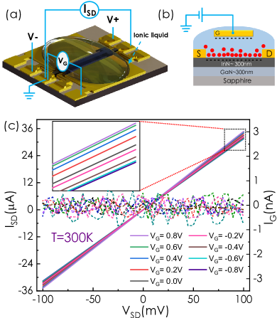
The InN samples were grown on sapphire substrates by plasma-assisted molecular beam epitaxy (PA-MBE) on c-oriented sapphire [24, 25, 26, 22] with negligible oxygen impurity demonstrated by the absence of oxygen O1s core level transition in XPS [24]. Patterned channels (Fig. 1(a)) on these were lithographically fabricated using as a hard mask layer followed by chlorine-based dry etching and subsequent removal of the hard-mask by . The devices had effective channel area of 1150 100 and thickness of 300 nm (Fig. 1(b)). Au/Ti (80 nm/20 nm) contacts were used for source (S) and drain (D) contacts. The gate electrode is much larger in area than the channel, eliminating the necessity of a reference electrode [6]. We used DEME-TFSI as the ionic liquid (IL). Contacts were covered with silicone gel during application of the IL. (See supplementary for detailed fabrication steps.). The ionic conductivity of DEME-TFSI are much higher than most other electrolytes [1]. The ionic liquid was cured in high vacuum at for hrs. All low-temperature measurements were carried out in a vacuum of mbar or better. Fig. 1(c), shows typical output characteristics (i.e. vs measurements) conducted at different gate voltages (), ranging from V to V with a step increment of V. The gate leakage remains times smaller than . The observed trends and direct Hall voltage measurements at , (as well as ), confirm that the carrier density is stable and indeed changes in a predictable way, allowing clear determination of the electron density () and mobility () from four terminal measurements. We recorded a change in carrier density with applied gate voltages, a finding of considerable relevance within the context of high carrier density systems [3, 27, 4, 28].
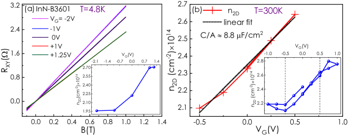
At a temperature of , we observe at = 0 V, yielding a mean free path (see Table 1). The capacitance determined from our measurements, approximately 8.8 as depicted in Fig. 2(b), surpasses what is achievable in MOSFET or HEMT-type devices. All low temperature measurements were performed below the glass transition temperature () of the ionic liquid (refer to supplementary data for the behavior of an ionic liquid gate). It is crucial to note that changing the gate voltage will have the desired effect only if done at . In our experiments, we always allowed the sample to warm up to room temperature for setting .
| () | ||||||||||
| -2 | 6.53 | 7.69 | 2.177 | 6.68 | 9.07 | 5.24 | 0.44229 | 38.82 | 0.0767 | |
| -1 | 6.56 | 7.71 | 2.174 | 6.69 | 9.30 | 5.38 | 0.44215 | 39.09 | 0.0745 | |
| 0 | 7.41 | 8.02 | 2.146 | 6.97 | 9.84 | 5.93 | 0.44090 | 40.73 | 0.0699 | |
| +1 | 9.00 | 8.56 | 2.087 | 7.44 | 9.52 | 6.12 | 0.43844 | 42.76 | 0.0649 | |
| +1.25 | 9.03 | 8.57 | 2.072 | 7.45 | 9.35 | 6.02 | 0.43779 | 43.06 | 0.0647 | |
| () | ||||||||||
| -3.25 | 5.11 | 7.09 | 2.074 | 6.15 | 6.15 | 3.27 | 0.43788 | 31.8 | 0.1214 | |
| 0 | 6.82 | 7.80 | 2.012 | 6.78 | 8.60 | 5.03 | 0.43519 | 37.2 | 0.0949 | |
| +0.5 | 7.07 | 7.90 | 2.004 | 6.86 | 8.26 | 4.90 | 0.43484 | 37.4 | 0.0937 | |
| +3.25 | 1.870 | 0.42887 |
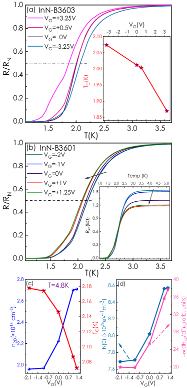
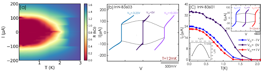
The superconducting critical temperature was measured in InN devices subjected to ionic liquid gating. The findings presented here stem from two such devices i.e. B3601 and B3603 (from two different wafers), demonstrating tunable superconducting parameters with variations in of and shown in Fig. 3 (a) & (b) respectively. The transition temperature of InN is primarily governed by carrier density rather than any disorder scattering () [29][30]. It has to be noted that we are able to both enhance and supress the in the same device. This cannot be explained by assuming a thin perturbed layer near the surface and a relatively unperturbed bulk superconductor in parallel. In such a case the resistive can be enhanced by a surface layer with a higher “short circuiting” the bulk, but cannot be suppressed by a layer with a lower , since the bulk superconductor would then act as a shorting path. Furthermore we see no evidence of a two step resistive transition that would indicate the presence of two parallel conducting layers. The perturbation of the superconducting state that we see thus is likely to be a state spanning the entire superconducting region of the stack.
We find reasonable agreement of the measured variation of the superconducting parameters with the expectations from a s-wave BCS superconductor having a simple free electron (density ) Fermi surface. The zero temperature coherence length for BCS s-wave superconductor is [31],
| (1) |
where, is the Fermi velocity and is the superconducting energy gap at , should vary as
| (2) |
The value of can be conveniently calculated from the critical field data (Fig. 4), the carrier density and are directly measured. This relation thus gives a good check on the consistency of the measurements, that does not require the exact constant of proportionality between and to be known. The calculated and measured values of differ by about which can be attributed to the disorder correction arising from a relatively small mean free path , that forces the observed to reduce to [32] [Chap 6]. Given that we have a correction of the order of what we observe is certainly expected. However given that , we do not expect any strong localisation effects or significant effects of granularity. This is also supported by hysteresis-free characteristics in the critical current measurements as shown in Fig. 5.
We thus consider free electron estimation of the density of states of at the Fermi level to be reasonable. This can be used to infer the variation of the strength of the attractive interaction , near the Fermi surface via the determination of by inverting the Eliashberg-McMillan eq.,
| (3) |
where is the Coulomb pseudopotential [33], which accounts for the electron-electron repulsive interaction and 370 K is the Debye temperature [34]. The coupling constant found here (1) suggests that behaves like a weak to medium coupling superconductor. Clearly, at lower carrier densities the pairing interaction strength gets stronger resulting in a higher as depicted in Fig. 3(c). The zero temperature coherence lengths calculated from the extrapolated values of the critical field ( Table-1), also mirror this increase of showing the superconducting state is stronger at lower carrier densities.
Furthermore, it is known that DOS is proportional to the slope of the upper critical field [35, 36, 37], i.e.
| (4) |
The calculated is shown in the right panel of Fig. 3(d) and compared with the free electron values exhibiting a very good agreement.
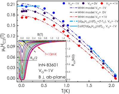
Next we looked into the temperature dependence of critical field. The magnetic field value (normal to the surface) at which the resistance of the superconductor attains half of its normal state value (the mean field value) is taken as critical field ( ). curves were fitted using the well-known Werthammer-Helfand-Hohenberg (WHH) model [35, 38] to understand the role of spin-orbit coupling (SOC), if present in the system, on the superconducting phase. WHH model gives the eq. 5.
| (5) |
where, , , is the Maki parameter, the dimensionless magnetic field == and is the spin-orbit scattering constant. The analysis reveals a small Maki parameter and virtually no impact of the spin-orbit term within the measured range of carrier densities (see Table 1). That is further confirmed by evaluating the limiting orbital field, , using the expression (T=0) . The calculated values closely correspond to the experimental data, as demonstrated for a gate voltage of (sky blue line) in the Fig. 4. In cases where spin-orbit coupling is strong, one obtains a high value of Maki parameter ( 2-3), as observed in our earlier work [39].
However there is one significant aspect in which an indicator of the strength of the superconducting state follows an opposing trend. In general the Landau-Ginzburg calculation of the critical current () of a thin film [32] [Chap 6] would predict a variation and hence approximately increase with . However we find that the application of a gate voltage either positive or negative substantially suppresses the critical current by as much as (see Fig. 5(b)). Many recent experiments demonstrated gate controlled critical current suppression in superconducting films [40, 41, 42, 43, 44]. A set of experiments suggest that critical current suppression is occurring due to Cooper pair breaking due to gate field [41, 40, 42]. Most likely the effect is due to modification of the electron distribution in the channel in response to the additional electric field arising from the gate. It is possible that the wavefunction as it either gets pulled towards the surface or as it gets pushed into the non-superconducting bulk region in fact sees regions with smaller normal-state mean free path and subsequent surface scattering and granularity effects leading to the suppression of the critical current.
The ability to change carrier density in a material to such an extent that the Fermi surface runs through a large volume of the Brillouin zone, potentially changing its shape from simple spherical or elliptical to more complex geometries incorporating nodes, necks, nesting vectors etc. does not exist as of now. For example in a simple tight binding on a square lattice, the Fermi surface changes from a simple circle to a square at half filling and then opens up. Development of techniques and materials in which potentially very large density modulations are possible are important as electron interaction driven phenomena inherently depend on the shape of the Fermi surface. In this paper, we have shown an example that can be a step forward in this direction.
Acknowledgements: We acknowledge support from Department of Science and Technology, Government of India under project: RD/0120-DSTIC01-001, Science and Engineering Research Board (SERB), Government of India under project: CRG/2018/001405. BCB acknowledges financial support through DST-INSPIRE fellowship of Govt. of India. We thank Amit P Shah (TIFR, Mumbai) for his assistance with the dry etch process and Prof. Saibal Sarkar (Department of Energy Science and Engineering, IIT Bombay) for providing access to deposit films. We thank Dr. Parushottam Majhi for useful discussions.
References
- Misra et al. [2007] R. Misra, M. McCarthy, and A. F. Hebard, Applied Physics Letters 90, 052905 (2007).
- Daghero et al. [2012] D. Daghero, F. Paolucci, A. Sola, M. Tortello, G. Ummarino, M. Agosto, R. Gonnelli, J. R. Nair, and C. Gerbaldi, Physical review letters 108, 066807 (2012).
- Petach et al. [2014] T. A. Petach, M. Lee, R. C. Davis, A. Mehta, and D. Goldhaber-Gordon, Physical Review B 90, 081108 (2014).
- Ueno et al. [2011] K. Ueno, S. Nakamura, H. Shimotani, H. Yuan, N. Kimura, T. Nojima, H. Aoki, Y. Iwasa, and M. Kawasaki, Nature nanotechnology 6, 408 (2011).
- Piatti et al. [2017] E. Piatti, D. Daghero, G. Ummarino, F. Laviano, J. Nair, R. Cristiano, A. Casaburi, C. Portesi, A. Sola, and R. Gonnelli, Physical Review B 95, 140501 (2017).
- Yuan et al. [2010] H. Yuan, H. Shimotani, J. Ye, S. Yoon, H. Aliah, A. Tsukazaki, M. Kawasaki, and Y. Iwasa, Journal of the American Chemical Society 132, 18402 (2010).
- Nakagawa et al. [2021] Y. Nakagawa, Y. Kasahara, T. Nomoto, R. Arita, T. Nojima, and Y. Iwasa, Science 372, 190 (2021).
- Walter et al. [2020] J. Walter, B. Voigt, E. Day-Roberts, K. Heltemes, R. M. Fernandes, T. Birol, and C. Leighton, Science advances 6, eabb7721 (2020).
- Ueno et al. [2008] K. Ueno, S. Nakamura, H. Shimotani, A. Ohtomo, N. Kimura, T. Nojima, H. Aoki, Y. Iwasa, and M. Kawasaki, Nature materials 7, 855 (2008).
- Hein et al. [1964] R. Hein, J. Gibson, R. Mazelsky, R. Miller, and J. Hulm, Physical Review Letters 12, 320 (1964).
- Smith and Stiles [1977] J. Smith and P. Stiles, Journal of Low Temperature Physics 26, 101 (1977).
- Ekimov et al. [2004] E. Ekimov, V. Sidorov, E. Bauer, N. Mel’Nik, N. Curro, J. Thompson, and S. Stishov, nature 428, 542 (2004).
- Bustarret et al. [2006] E. Bustarret, C. Marcenat, P. Achatz, J. Kačmarčik, F. Lévy, A. Huxley, L. Ortéga, E. Bourgeois, X. Blase, D. Débarre, et al., Nature 444, 465 (2006).
- Miura et al. [1997] N. Miura, H. Ishii, A. Yamada, M. Konagai, Y. Yamauchi, and A. Yamamoto, Japanese journal of applied physics 36, L256 (1997).
- Inushima et al. [2001] T. Inushima, V. Vecksin, S. Ivanov, V. Davydov, T. Sakon, and M. Motokawa, physica status solidi (b) 228, 9 (2001).
- Inushima et al. [2006] T. Inushima, N. Kato, D. K. Maude, H. Lu, W. Schaff, R. Tauk, Y. Meziani, S. Ruffenack, O. Briot, W. Knap, et al., physica status solidi (b) 243, 1679 (2006).
- Yuan et al. [2009] H. Yuan, H. Shimotani, A. Tsukazaki, A. Ohtomo, M. Kawasaki, and Y. Iwasa, Advanced Functional Materials 19, 1046 (2009).
- Glover III and Sherrill [1960] R. Glover III and M. Sherrill, Physical Review Letters 5, 248 (1960).
- Stadler [1965] H. Stadler, Physical Review Letters 14, 979 (1965).
- Choi et al. [2014] J. Choi, R. Pradheesh, H. Kim, H. Im, Y. Chong, and D.-H. Chae, Applied Physics Letters 105 (2014).
- Piatti et al. [2016] E. Piatti, A. Sola, D. Daghero, G. A. Ummarino, F. Laviano, J. R. Nair, C. Gerbaldi, R. Cristiano, A. Casaburi, and R. S. Gonnelli, Journal of Superconductivity and Novel Magnetism 29, 587 (2016).
- Pal et al. [2018] B. Pal, B. P. Joshi, H. Chakraborti, A. K. Jain, B. K. Barick, K. Ghosh, A. Laha, S. Dhar, and K. D. Gupta, in AIP Conference Proceedings, Vol. 1942 (AIP Publishing, 2018).
- Jones et al. [2006] R. Jones, K. Yu, S. Li, W. Walukiewicz, J. Ager, E. Haller, H. Lu, and W. Schaff, Physical Review Letters 96, 125505 (2006).
- Ghosh et al. [2017] K. Ghosh, J. S. Rathore, and A. Laha, Superlattices and Microstructures 101, 405 (2017).
- Barick et al. [2016] B. K. Barick, N. Prasad, R. K. Saroj, and S. Dhar, Journal of Vacuum Science & Technology A 34 (2016).
- Barick et al. [2018] B. Barick, R. K. Saroj, N. Prasad, D. Sutar, and S. Dhar, Journal of Crystal Growth 490, 104 (2018).
- Sagmeister et al. [2006] M. Sagmeister, U. Brossmann, S. Landgraf, and R. Würschum, Physical review letters 96, 156601 (2006).
- Prassides [2011] K. Prassides, Nature nanotechnology 6, 400 (2011).
- Dubi et al. [2007] Y. Dubi, Y. Meir, and Y. Avishai, Nature 449, 876 (2007).
- Ghosal et al. [1998] A. Ghosal, M. Randeria, and N. Trivedi, Physical review letters 81, 3940 (1998).
- Tinkham [2004] M. Tinkham, Introduction to superconductivity (Courier Corporation, 2004).
- De Gennes [2018] P.-G. De Gennes, Superconductivity of metals and alloys (CRC press, 2018).
- McMillan [1968] W. McMillan, Physical Review 167, 331 (1968).
- Davydov et al. [1999] V. Y. Davydov, V. Emtsev, I. Goncharuk, A. Smirnov, V. Petrikov, V. Mamutin, V. Vekshin, S. Ivanov, M. Smirnov, and T. Inushima, Applied physics letters 75, 3297 (1999).
- Werthamer et al. [1966] N. Werthamer, E. Helfand, and P. Hohenberg, Physical Review 147, 295 (1966).
- Guo et al. [2004] Y. Guo, Y.-F. Zhang, X.-Y. Bao, T.-Z. Han, Z. Tang, L.-X. Zhang, W.-G. Zhu, E. Wang, Q. Niu, Z. Qiu, et al., Science 306, 1915 (2004).
- Chockalingam et al. [2008] S. Chockalingam, M. Chand, J. Jesudasan, V. Tripathi, and P. Raychaudhuri, Physical Review B 77, 214503 (2008).
- Helfand and Werthamer [1966] E. Helfand and N. Werthamer, Physical Review 147, 288 (1966).
- Chakraborti et al. [2022] H. Chakraborti, B. P. Joshi, C. K. Barman, A. K. Jain, B. Pal, B. C. Barik, T. Maiti, R. Schott, A. D. Wieck, M. Prasad, et al., Applied Physics Letters 120 (2022).
- Rocci et al. [2020] M. Rocci, G. De Simoni, C. Puglia, D. D. Esposti, E. Strambini, V. Zannier, L. Sorba, and F. Giazotto, ACS nano 14, 12621 (2020).
- De Simoni et al. [2018] G. De Simoni, F. Paolucci, P. Solinas, E. Strambini, and F. Giazotto, Nature nanotechnology 13, 802 (2018).
- Paolucci et al. [2021] F. Paolucci, F. Crisá, G. De Simoni, L. Bours, C. Puglia, E. Strambini, S. Roddaro, and F. Giazotto, Nano letters 21, 10309 (2021).
- Golokolenov et al. [2021] I. Golokolenov, A. Guthrie, S. Kafanov, Y. A. Pashkin, and V. Tsepelin, Nature Communications 12, 2747 (2021).
- Alegria et al. [2021] L. D. Alegria, C. G. Bøttcher, A. K. Saydjari, A. T. Pierce, S. H. Lee, S. P. Harvey, U. Vool, and A. Yacoby, Nature Nanotechnology 16, 404 (2021).
See pages - of SM.pdf