Effective removal of global tilt from topography images of vicinal surfaces with narrow terraces
Abstract
The main feature of vicinal surfaces of crystals characterized by the Miller indices , is rather small width (less than 10 nm) and substantially large length (more than 200 nm) of atomically-flat terraces on sample surface. This makes difficult to apply standard methods of image processing and correct visualization of crystalline lattice at the terraces and multiatomic steps. Here we consider two procedures allowing us to minimize effects of both small-scale noise and global tilt of sample: (i) analysis of the difference of two Gaussian blurred images, and (ii) subtraction of the plane, whose parameters are determined by optimization of the histogram of the visible heights, from raw topography image. It is shown that both methods provide non-distorted images demonstrating atomic structures on vicinal Si(5 5 6) and Si(5 5 7) surfaces.
∗ Corresponding author, e-mail address: aladyshkin@ipmras.ru
I Introduction
Scanning tunneling microscopy (STM) is unique experimental technique providing detailed information about local structural and electronic properties of surfaces of solids. Binnig-82 ; Chen-93 ; Voigtlaender-15 However raw topography images are usually distorted due to global tilt of sample, non-orthogonality of fast- and slow-scanning directions of piezo-scanner, creep of piezo ceramics leading to non-controlled drift of scanning area etc. As a consequence, raw topography images require justified corrections. Global tilt of the sample with respect to the reference coordinate system can be routinely removed by subtraction of an approximate plane, parameters of which can be determined by considering any of atomically-flat terraces of rather large size. Distortions in the lateral directions caused by creep and thermal drift can be compensated afterwards provided that scanning area incorporated some fragments of crystalline lattice with well-known structure like Si(1 1 1), Si(1 1 1) or graphite honeycomb lattice. Such the correction procedures are incorporated in commercial and free-distributed applications like WsXM,wsxm-ref Gwyddion gwyddion-ref and others.
This paper is devoted to the problem of reliable elimination of the global tilt for samples with vicinal surfaces. Vicinal or high-Miller-index stepped surface Oura-03 is crystalline surface, which is misoriented from closely-packed low-Miller-index plane by a small angle (see comment Comment ). As a result, such surface can be viewed as a periodic combination of atomically-flat low-Miller-index terraces and mono- or multiatomic steps between them. Vicinal Si() surfaces seem to be perspective semiconducting substrates for fabrication of ordered low-dimensional systems with unique electronic structure, transport and magnetic properties.Erwin-10 ; Losio-01 ; Ahn-PRL-03 ; Lipton-Duffin-08 ; Tegenkamp-05 ; Morikawa-10 ; Brand-15 ; Quentin-20 ; Nita-22 Such array of terraces and steps can be considered both as natural cheap and reproducible quantum standards of distances and heights and as perspective substrates for deposition of ultra-thin metallic films and design of quasi-one-dimensional metallic wires. Losio-01 ; Ahn-PRL-03 ; Lipton-Duffin-08 ; Tegenkamp-05 ; Morikawa-10 ; Brand-15 ; Quentin-20 It was demonstrated Kirakosian-APL-01 that the formation of atomically-precise ordered array of Si(1 1 1) terraces and quantized steps, whose heights are equal to three interplane distances (so called triple steps), is possible on Si(5 5 7) surface with typical lateral dimensions of the order of nm.
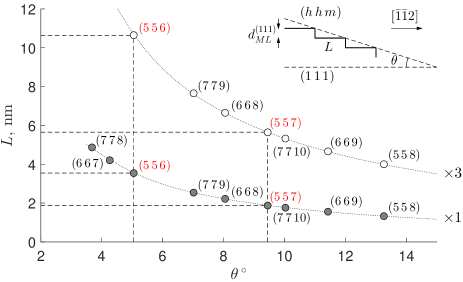
The main problem in processing topography images of clean vicinal surfaces is related to the fact that the atomically-flat terraces are rather narrow, what introduces substantial uncertainty in estimating the parameters of the approximate plane and thus complicates accurate elimination of the global tilt using standard procedures. Indeed, the period of series of identical multiatomic steps can be calculated using the following relationship (see inset in figure 1)
| (1) |
where is the interplane distance (or thickness of a monolayer) for a family of nearest closely-packed terraces, is the multiplicity factor. The dependence on for several types of vicinal surfaces of Si single crystals is presented in figure 1. It is easy to see that the widths of the (1 1 1) terraces between monatomic steps on vicinal surfaces Si(5 5 6) and Si(5 5 7) are quite small (3.55 nm and 1.88 nm, respectively).
Despite the standard procedure of subtraction of the plane from raw topography image for Si single crystals with narrow terraces is badly conditioned, some authors have successfully applied this method for visualization of atomic structure of vicinal surfaces.Chaika-APL-09 Some authors seemingly considered misaligned topography images expecting that the presence of tilted terraces on topography images does not affect their scientific conclusions.Teys-06 ; Zhachuk-09 ; Zhachuk-14 ; Chaika-SurfSci-09 ; Kim-10 ; PerezLeon-16 ; PerezLeon-17 ; Oh-08 Kirakosian et al. Kirakosian-APL-01 have applied procedure of numerical differentiation of topography signal along the fast-scanning direction to visualize atomic structure on step-like Si(5 5 7) surface. However, this approach apparently converts raw topography data into a picture with distorted contrast, which cannot be referred to actual crystalline lattice. Numerical differentiation of the STM images was also used in other studies.Chaika-JAP-09 In order to balance contrast along the multiatomic steps, Pérez León et al. PerezLeon-17 have subtracted linear fit for each line in raw topography image. Apparently, this method works only if the step edges on the rotated topography image are parallel to horizontal direction.
Some methods suitable for the considered problem were developed by scientists working in fields of image processing/recognition and computer vision (see, e.g., Ref.Gonsales-04 ). The approach known as the difference-of-gaussians Gonsales-04 ; Kovasznayl-53 ; Marr-80 ; Lindeberg-15 is frequently used for automatic detection of defects, lines and edges on halftone and pseudocolor images. Recently this approach was used for electron microscopyKrivanek-15 ; Misra-20 and atomic-force microscopyMarsh-15 image processing. To the best of our knowledge, this simple and handy method was never applied for problems of scanning tunneling microscopy in general and for the processing of topography of vicinal surfaces in particular. One of our goals is to introduce this well-known method to the surface-science community dealing with complicated topography images of non-flat surfaces with steps, facets, bubbles etc (see also Aladyshkin-submitted ). To illustrate better capabilities of the difference-of-gaussians approach we present the analysis of raw topography images of vicinal Si(5 5 6) and Si(5 5 7) surfaces with one-dimensional arrays of triple steps.Kirakosian-APL-01 ; Chaika-APL-09 ; Teys-06 ; Zhachuk-09 ; Zhachuk-14 ; Chaika-SurfSci-09 ; Oh-08 ; Chaika-JAP-09 ; Henzler-03
The second part of the paper is devoted to the description of a histogram-based method of alignment of raw topography images. The idea is quite simple: one can determine the proper parameters of the plane, which should be subtracted from raw data, by minimizing the widths of the peaks for the probability density function , characterizing the statistical distribution of the visible heights for partly aligned images. We demonstrate that this algorithm can be easily realized in any programming language. This approach allows us to analyze both two-dimensional periodicity for atomically-flat terraces and precisely estimate the heights of multiatomic steps. We hope that this new method will be convenient for automatic analysis of large datasets of raw topography images.
II Experimental procedure
Experimental investigations of crystalline structure of vicinal Si(5 5 6) and Si(5 5 7) surfaces were carried out in an ultrahigh vacuum (UHV) scanning tunneling microscope GPI-300 (scan) operating at a base vacuum pressure of mbar. All STM measurements were performed at room temperature in the regime of constant tunneling current and fixed electrical potential of the sample with respect to a grounded probe. Electrochemically etched poly- and single crystalline W tips were used as STM probes after in situ electron bombardment and ion etching in UHV chamber.Chaika-SciRep-14 Free-distributed applications WsXM wsxm-ref and Gwyddion gwyddion-ref as well as original programs written by authors in Matlab and Python were used for processing of topography images.
Si samples with typical dimensions of 0.5 mmmm mm were made from polished -type single-crystal Si(5 5 6) and Si(5 5 7) wafers (P-doped, resistivity of the order of cm at 300 K). These samples were first outgassed at moderate temperatures (C) for 15-20 hours inside UHV chamber in order to remove contaminations from sample and contact plates without damaging natural oxide layer at the sample surface. For preparing clean surfaces with periodic step array we used the procedure of in situ direct-current annealing (current is oriented perpendicular to steps and it flows in step-up direction). This procedure allows us to reproducibly fabricate periodic array of triple steps at the sample surface of large (micron-size) areas (figure 2). Note that prolonged annealing at higher temperatures at the final stage leads to substantial increase in widths of atomically-flat Si(1 1 1) terraces and formation of macrosteps in some surface areas similar to that described by Latyshev and Aseev.Latyshev-98
III Results and discussion
III.1 1. Extraction of periodic signal associated with surface reconstructions
We start with a trivial remark that the convolution of an arbitrary function with a Gaussian function
| (2) |
plays pole of a low-pass filter, which effectively weakens Fourier components in the spectrum of with large values exceeding certain threshold value of the order of , where is the width of the Gaussian filter. In the other words, the Gaussian blurring suppresses small-scale noisy components without affecting medium-scale and large-scale components.
Let us consider a function of two variables , which can be associated with raw topography image, acquired by scanning tunneling microscopy. Generally speaking, this function can have (i) small-scale noisy component, (ii) periodic two-dimensional (2D) component due to a presence of crystalline lattice, and (iii) large-scale inhomogeneities due to global tilt of the sample, multiatomic steps on surface, internal stress etc.
We introduce the difference of two blurred images prepared by the convolutions of raw topographic image and two Gaussian functions of various widths and
| (3) |
It is easy to show that the procedure (3) corresponds to band-pass filtering in -space and it is equivalent to numerical calculation of the Laplacian of the blurred function. Aladyshkin-submitted This difference-of-gaussians method is frequently used in image processing for automatic detection of edges, defects etc.Gonsales-04 ; Kovasznayl-53 ; Marr-80 ; Lindeberg-15 We apply this approach to get rid of noisy component and global slope in topographical images and thus to highlight both periodic 2D corrugation associated with surface reconstructions on terraces. In addition, this method makes possible to study irregular atomic structure at multiple steps which would be hidden in usual topography STM images because of large step height substantially exceeding typical atomic corrugations at steps and terraces. The strategy of choosing the parameters and is rather simple: should be of the order of pixel size, while should be larger than but smaller than typical length scale of structural inhomogeneities.
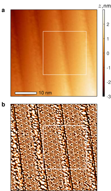
Examples of extraction of the periodic components, associated with 2D reconstructions on the Si(1 1 1) terraces, from raw topography images for the Si(5 5 6) surface by means of the difference-of-gaussians procedure (3) are presented in figures 3b and 4. Since the observed period of the steps on the Si(5 5 6) surface is close to 10 nm (figure 3b), we conclude that these steps should be triple ones.
We would like to emphasize that the procedure (3) is rather robust and it seems to be not very sensitive to particular values of the smoothing parameters and . Indeed, increasing in the value (for the fixed parameter) leads to change in contrast for the map of the differential signal without modification of the periodic components related to the reconstruction on the terraces and the periodicity of the step array (figure 4). We can only mention that changing the to ratio one can enhance/lessen various details in topography images that can be practically used for direct visualization and precise analysis of STM data obtained on vicinal surfaces. For example, the differential signal obtained at to ratios equal to 2:1 and 5:1 (figure 4a,b) can be used for simultaneous visualization of the terrace and step atomic rows with comparable contrast despite the large height difference related to the presence of multiple steps on the surface. This cannot be achieved using plane or other standard correction procedures generally used for STM image processing. Contrary to typical differentiated STM images (e. g., ), maps of the differential signal reproduce well all details of the atomic structure with exactly the same positions of maxima and minima as it could be observed on perfectly aligned topography image (figures 3b and 4). Thus, the difference-of-gaussians maps provide correct visualization of topography images projected onto scanning plane irrespective to particular large-scale tilt in various areas of considered surface.
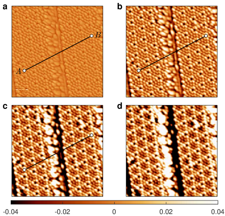
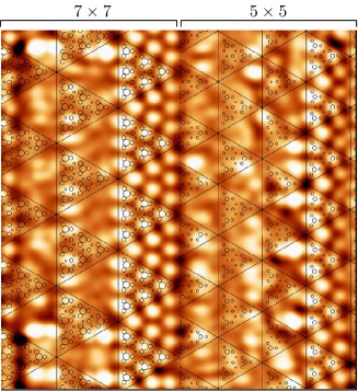
For Si() surfaces with reconstructed terraces, the map without global tilt can be easily utilized for image correction (e. g., by means of affine transformations) based on the well-known lattice parameters and experimentally measured values. Afterwards, the corrected images can be used for precise determination of distances between features of interest and periodicity of the step array. This can hardly be done using tilted topography images because only a fraction of the image can be visualized after contrast level adjustments while some image areas remain invisible. For example, the atomic structure of vicinal Si(5 5 7) surface with regular array of triple steps was disputed in literature Kirakosian-APL-01 ; Teys-06 ; Zhachuk-09 ; Oh-08 ; Chaika-APL-09 despite the high-quality topography images were acquired by different groups. Using the atomically-resolved differential map of the regular triple step array on Si(5 5 7) wafers (figure 2) we remove uncontrollable STM image distortions using the well-known parameters of the unit cell. An example of the affine-corrected map obtained for the Si(5 5 7) surface with triple step array is presented on figure 5. The left part of this image shows rather good coincidence between the adatom positions on the reconstructed terrace observed experimentally and model structure Oura-03 . At the same time, the right part of the image in figure 5 demonstrates the presence of -reconstruction on the flat terrace between triple steps Chaika-APL-09 . The model Oura-03 overlaid onto the right part of the map also shows coincidence of the experimentally measured features with the model atomic structure. Using this map, we define the periodicity of the Si(557) triple step array from either left or right part of the image having different step structure and terrace reconstructions. The distance between neighboring grooves is the same for both structures ’Si(1 1 1) terrace + triple step’ and ’Si(1 1 1) terrace + triple step’ with precision of one interatomic-row distance in the direction perpendicular to the step edges.
III.2 2. Removal of a background signal associated with global tilt of the sample
The procedure of semi-automatic removal of the global tilt described below consists of three stages. The program is written in Matlab programming language, typical execution time is about 10 s.
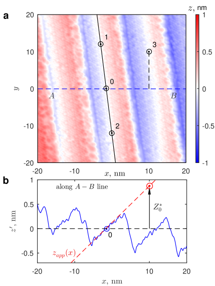
At the first stage we determine three reference points (e. g., by clicks of a mouse) in such a way that the points 1 and 2 should be positioned at the same atomically-flat terrace, while the point 3 can be located at any place excluding the line (see figure 6a). Using the coordinates of the reference points , and one can calculate the parameters of the plane
| (4) |
passing through these points, where
| (5) |
The result of the subtraction of the plane (4) from raw topography image (figure 3a)
| (6) |
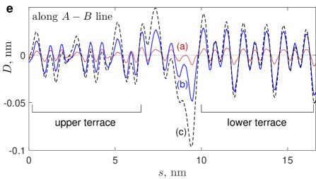
is shown in figure 6a. We will refer to as tilted topography image. If there are no small-scale corrugation, noise and outliers, the line for the tilted image apparently belongs to the plane . It is important to note that the procedure (5)–(6) minimizes the global slope in the direction along the atomically-flat terraces.
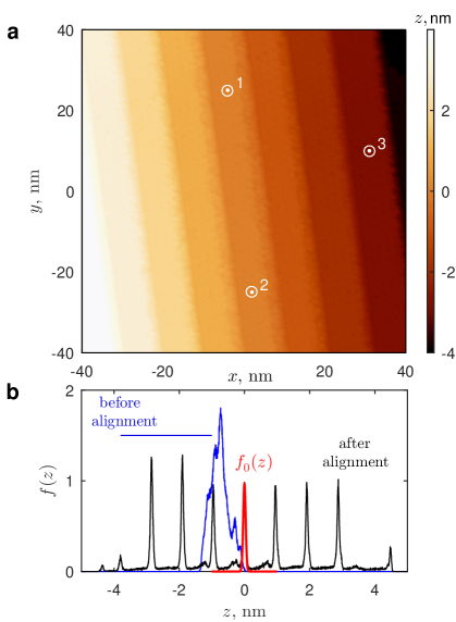
At the second stage we estimate an offset, what is needed to shift the reference point in the vertical direction in order to get an aligned topography image with horizontal terraces. We define the point 0 as a middle point of the line segment and then plot the profile of the tilted surface along the fast-scanning direction (i. e. along the axis) through this point (figure 6b). We introduce local linear extrapolation
| (7) |
The dependence of is shown in figure 6b by dashed line and it evidences for the pronounced global tilt of the topography image along the axis at the angle of 4.3∘. We can define the auxiliary parameter as the difference between the extrapolated value for the dependence at the reference point 3 and zero level (red dot in figure 6b). It is clear that the repeated subtraction of a plane defined by the points , and from the titled image , prepared at the first stage, is able to return us a topography image without noticeable slope in the direction. Unfortunately, this method seems to be ineffective for noisy topography images containing atomically-flat terraces of nanometer-size widths because of substantial uncertainty in estimating the position of the offset .
In order to overcome this issue, at the third stage we numerically solve single-parameter optimization problem:
(i) for each value, taken in the vicinity of , one can introduce a trial plane defined by the points , , and .
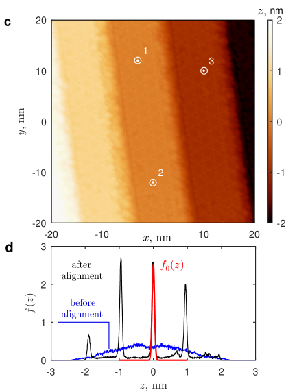
(ii) after subtraction this trial plane from the tilted topography image prepared at the first stage, one can compose a histogram , which characterizes the distribution of visible heights for such partly aligned topographical image. The probability distribution function for properly aligned image should have a series of narrow peaks (see figure 6d), and one of these peaks should be definitely positioned at (so called zero peak). The zero peak can be fitted by a Gaussian function
| (8) |
where and are fitting parameters. Similar histogram-based analysis was already applied for precise determination of the height of monatomic steps on Si(1 1 1) surface and subsequent fine calibration of a piezo-scanner Aladyshkin-23 .
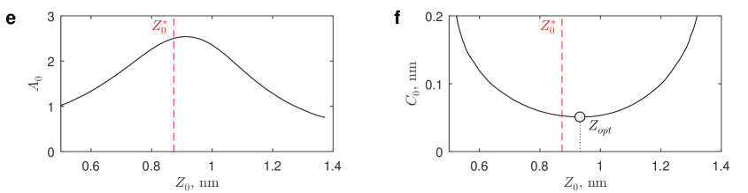
(iii) after sweeping , one can get the dependences of the amplitude and the width of the zero peak on the parameter (figures 6e and 6f, respectively).
We define the optimum offset value as the value at which the zero peak has the minimal width. The results of the additional subtraction of the optimal plane running through the points (), () and (), from the tilted image (figure 6a)
| (9) |
is presented in figures 6c;
| (10) |
Thus, we are able to compose the aligned topography image, which has constant (with experimental accuracy) magnitude at each atomically-flat terrace. The aligned topography image for larger scanning area of the Si(5 5 6) surface is shown in 7a.
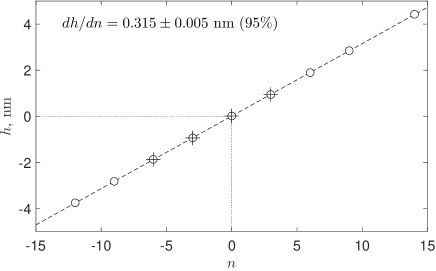
As expected, the probability density functions for these images have series of narrow maxima (figures 6d and 7b), whose width (nm) is substantially smaller than the interval between neighbor maxima (nm). Statistical analysis of the mutual arrangement of the peaks at these histograms, illustrating relative heights of the multiatomic steps of the aligned Si(5 5 6) surfaces, is presented in figure 8. We conclude that the most part of the steps at the Si(5 5 6) surfaces are triple steps, which have mean height close to the theoretical value nm, where nm is the thickness of monolayer for the Si(1 1 1) surface.
The difference of the aligned topographic image (without global tilt both along - and -directions) and background signal, associated with the series of quantized steps on the sample surface, can be introduced as follows
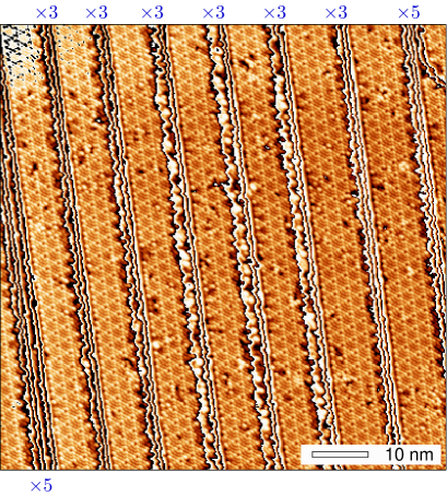
| (11) |
where symbol denotes the function which rounds each element in the argument to the nearest integer. Example of applying the procedure (11) to the aligned image in figure 7a is shown in figure 9. It is easy to see that this transformation allows to visualize the crystalline lattices at each terrace and determine multiplicity factors for each multiatomic steps at the surface. The latter factor is apparently equal to the number of almost parallel lines running along the steps. Such histogram-based optimization procedure is very useful for experimental studies oriented to the precise determination of the parameters of mono- and multiatomic steps, for example, for the investigation of the bias dependence of the visible height of the monatomic steps in thin Pb(1 1 1) films Aladyshkin-23 . Similarly to the images obtained using the difference-of-gaussians approach (figure 5), such aligned image can be affine corrected and further utilized for precise determination of the step periodicity and lateral shifts of the surface unit cells in neighboring terraces.
IV Conclusion
We report on successful implementation of two simple algorithms allowing us to eliminate global slope of sample and to visualize crystalline structure on vicinal Si(5 5 6) and Si(5 5 7) surfaces with rather narrow atomically-flat terraces. The first method (also known as difference of gaussians) is simply remove local slope, associated by large-scale inhomogeneities, from raw topography image. As a result, small-scale corrugations for all tilted terraces become shifted to the plane regardless on actual height and slope of particular terrace, what can be very useful for visualization of lower-lying features in topography images and further detailed analysis by fast Fourier transform. The second method is based on single-parameter optimization problem in seeking the coefficients of the optimal plane, which characterizes the global slope of the sample, by considering the histogram of visible heights and minimizing the width of the peaks on this histogram. After the subtraction of the optimal plane from raw topography image, one can prepare aligned image with horizontal terraces. Further analysis applied to the aligned images makes possible to visualize crystalline structure on vicinal surfaces, precisely define the distances between step edges, and determine miltiplicity factor for all multiatomic steps on the sample surface.
V Acknowledgements
This work was funded by the Russian State Contracts for the Osipyan Institute of Solid-State Physics RAS (sample preparation and measurements) and for the Institute for Physics of Microstructures RAS (no. FFUF-2024-0020, programming and data analysis).
References
References
- (1) G. Binnig, H. Rohrer, Ch. Gerber, and E. Weibel, Tunneling through a controllable vacuum gap // Appl. Phys. Lett., vol. 40, 178 (1982); doi: 10.1063/1.92999.
- (2) C. J. Chen, Introduction to scanning tunneling microscopy. Oxford University Press, New York, 412 p (1993).
- (3) B. Voigtländer, Scanning Probe Microscopy: Atomic Force Microscopy and Scanning Tunneling Microscopy, Springer-Verlag GmbH Berlin Heidelberg, 382 p. (2015).
- (4) I. Horcas, R. Fernandez, J.M. Gomez-Rodriguez, J. Colchero, J. Gomez-Herrero and A. M. Baro, WSXM: A software for scanning probe microscopy and a tool for nanotechnology // Rev. Sci. Instrum. vol. 78, 013705 (2007); doi: 10.1063/1.2432410; http://wsxm.eu.
- (5) D. Nečas and P. Klapetek, Gwyddion: an open-source software for SPM data analysis // Central European Journal of Physics, vol. 10, 181–188 (2012); doi: 10.2478/s11534-011-0096-2; http://gwyddion.net.
- (6) K. Oura, V. G. Lifshits, A. V. Zotov, A. A. Saranin, M. Katayama, Surface Science: An Introduction, Springer-Verlag, 452 p. (2003)
-
(7)
The angle between two planes,
characterized by the Miller indices (, , ) and (, , ), can be determited from the relationship
- (8) S. C. Erwin and F. J. Himpsel, Intrinsic magnetism at silicon surfaces // Nat. Commun., vol. 1, 58 (2010); doi: 10.1038/ncomms1056.
- (9) R. Losio, K. N. Altmann, A. Kirakosian, J.-L. Lin, D. Y. Petrovykh, and F. J. Himpsel, Band splitting for Si(5 5 7)-Au: Is it spin-charge separation? // Phys. Rev. Lett., vol. 86, 4632 (2001); doi: 10.1103/PhysRevLett.86.4632.
- (10) J. R. Ahn, H. W. Yeom, H. S. Yoon, and I.-W. Lyo, Metal-insulator transition in Au atomic chains on Si with two proximal bands // Phys. Rev. Lett., vol. 91, 196403 (2003); doi: 10.1103/PhysRevLett.91.196403.
- (11) J. A. Lipton-Duffin, A. G. Mark, J. M. MacLeod, and A. B. McLean, Si(5 5 7)-Ag: A metallic quasi-one-dimensional system // Phys. Rev. B, vol. 77, 125419 (2008); doi: 10.1103/PhysRevB.77.125419.
- (12) C. Tegenkamp, Z. Kallassy, H. Pfnür, H.-L. Günter, V. Zielasek, and M. Henzler, Switching between one and two dimensions: Conductivity of Pb-induced chain structures on Si(5 5 7) // Phys. Rev. Lett., vol. 95, 176804 (2005); doi: 10.1103/PhysRevLett.95.176804.
- (13) H. Morikawa, K. S. Kim, Y. Kitaoka, T. Hirahara, S. Hasegawa, H. W. Yeom, Conductance transition and interwire ordering of Pb nanowires on Si(5 5 7) //Phys. Rev. B, vol. 82, 045423 (2010); doi: 10.1103/PhysRevB.82.045423.
- (14) C. Brand, H. Pfnür, G. Landolt, S. Muff, J. H. Dil, T. Das and C. Tegenkamp, Observation of correlated spin–orbit order in a strongly anisotropic quantum wire system // Nat. Commun., vol. 6, 8118 (2015); doi: 10.1038/ncomms9118.
- (15) M. Quentin, T. T. Nhung Nguyen, H. Pfnür, and C. Tegenkamp, Electronic correlation effects in Pb quantum wires on Si(5 5 7) // Phys. Rev. B, vol. 102, 035438 (2020); doi: 10.1103/PhysRevB.102.035438.
- (16) P. Nita, M. Dachniewicz, M. Jałochowski, K. Palotas, and M. Krawiec, Template driven self-assembly of the pentacene structure on the Si(5 5 3)-Pb surface // J. Phys. Chem. C, vol. 126, 17738-17745 (2022); doi: 10.1021/acs.jpcc.2c05308.
- (17) A. Kirakosian, R. Bennewitz, J. N. Crain, Th. Fauster, J.-L. Lin, D. Y. Petrovykh, and F. J. Himpsel, Atomically accurate Si grating with 5.73 nm period // Appl. Phys. Lett., vol. 79, 1608 (2001); doi: 10.1063/1.1401788.
- (18) A. N. Chaika, V. N. Semenov, V. G. Glebovskiy and S. I. Bozhko, Scanning tunneling microscopy with single crystalline W[0 0 1] tips: High resolution studies of Si(5 5 7) surface // Appl. Phys. Lett., vol. 95, 173107 (2009); doi: 10.1063/1.3254240.
- (19) S. A. Teys, K. N. Romanyuk, R. A. Zhachuk, and B. Z. Olshanetsky, Orientation and structure of triple step staircase on vicinal Si(1 1 1) surfaces // Surf. Sci., vol. 600, 4878 (2006); doi: 10.1016/j.susc.2006.08.009.
- (20) R. Zhachuk, S. Pereira, Comment on ’Atomic structure model of the reconstructed Si(557) surface with a triple step structure: Adatom-parallel dimer model’ // Phys. Rev. B, vol. 79, 077401 (2009); doi: 10.1103/PhysRevB.79.077401.
- (21) R. Zhachuk, S. Teys, J. Coutinho, M.J. Rayson, P.R. Briddon, Static and dynamic buckling of reconstructions at triple steps on Si(1 1 1) surfaces // Appl. Phys. Lett., vol. 105, 171602 (2014); doi: 10.1063/1.4900783.
- (22) A. N. Chaika, D. A. Fokin, S. I. Bozhko, A. M. Ionov, F. Debontridder, T. Cren, D. Roditchev, Atomic structure of a regular Si(2 2 3) triple step staircase // Surf. Sci. 603, vol. 752 (2009); doi: 10.1016/j.susc.2009.01.007.
- (23) M. K. Kim, D.-H. Oh, J. Baik, C. Jeon, I. Song, J. H. Nam, S. H. Woo, C.-Y. Park, and J. R. Ahn, Control of a quasi-one-dimensional phase of a Si nanostructure: Vicinal Si(5 5 7) surfaces // Phys. Rev. B, vol. 81, 085312 (2010); doi: 10.1103/PhysRevB.81.085312.
- (24) C. Pérez León, H. Drees, S. M. Wippermann, M. Marz, and R. Hoffmann-Vogel, Atomic-scale imaging of the surface dipole distribution of stepped surfaces // J. Phys. Chem. Lett., vol. 7, 426 (2016); doi: 10.1021/acs.jpclett.5b02650.
- (25) C. Pérez León, H. Drees, S. M. Wippermann, M. Marz, and R. Hoffmann-Vogel, Atomically resolved scanning force studies of vicinal Si(1 1 1) // Phys. Rev. B, vol. 95, 245412 (2017); doi: 10.1103/PhysRevB.95.245412.
- (26) D.-H. Oh, M. K. Kim, J. H. Nam, I. Song, C.-Y. Park, S. H. Woo, H.-N. Hwang, C. C. Hwang, and J. R. Ahn, Atomic structure model of the reconstructed Si(5 5 7) surface with a triple step structure: Adatom-parallel dimer model // Phys. Rev. B, vol. 77, 155430 (2008); 10.1103/PhysRevB.77.155430.
- (27) A. N. Chaika, D. A. Fokin, S. I. Bozhko, A. M. Ionov, F. Debontridder, V. Dubost, T. Cren, D. Roditchev, Regular stepped structures on clean Si() surfaces // J. Appl. Phys., vol. 105, 034304 (2009); doi: 10.1063/1.3072667.
- (28) R. C. Gonlases, R. E. Woods, S. L. Eddins, Digital image processing using MATLAB, 2nd ed., Tata McGraw Hill Education Private Limited, New Delhi, 728 p. (2010).
- (29) I. S. G. Kovasznayl, H. M. Joseph, Processing of Two-Dimensional Patterns by Scanning Techniques // Science, v. 118, 475-477 (1953); doi: 10.1126/science.118.3069.47.
- (30) D. Marr and E. Hildreth, Theory of Edge Detection // Proc. R. Soc. Lond. B, vol. 207, 187-217 (1980); doi: 10.1098/rspb.1980.0020.
- (31) T. Lindeberg, Image Matching Using Generalized Scale-Space Interest Points // J. Math. Imaging Vis., vol. 52, 3–36 (2015) ; doi: 10.1007/s10851-014-0541-0.
- (32) O. L. Krivanek, M.F. Chisholm, V. Nicolosi, T. J. Pennycook, G. J. Corbin, N. Dellby, M. F. Murfitt, C. S. Own, Z. S. Szilagyi, M. P. Oxley, S. T. Pantelides, S. J. Pennycook, Atom-by-atom structural and chemical analysis by annular dark-field electron microscopy // Nature, v. 464, 571–574 (2010); https://doi.org/10.1038/nature08879.
- (33) S. Misra, Y. Wu, Machine learning assisted segmentation of scanning electron microscopy images of organic-rich shales with feature extraction and feature ranking, chapter 10 in book: S. Misra, H. Li, J. He, Machine Learning for Subsurface Characterization, Elsevier, Gulf Professional Publishing, p. 289-314 (2020); ISBN 978-0-12-817736-5; doi:10.1016/B978-0-12-817736-5.00010-7.
- (34) B. P. Marsh, N. Chada, R. R. S. Gari, K. P. Sigdel, G. M. King, The Hessian Blob Algorithm: Precise Particle Detection in Atomic Force Microscopy Imagery // Sci. Rep., v. 8, 978 (2018); doi: 10.1038/s41598-018-19379-x.
- (35) M. Henzler, R. Zhachuk, The step structure of the Si(5 5 7) surface // Thin Solid Films, vol. 428, 129 (2003); 10.1016/S0040-6090(02)01236-1.
- (36) A. N. Chaika, N. N. Orlova, V. N. Semenov, E. Yu. Postnova, S. A. Krasnikov, M. G. Lazarev, S. V. Chekmazov, V. Yu. Aristov, V. G. Glebovsky, S. I. Bozhko and I. V. Shvets, Fabrication of [0 0 1]-oriented tungsten tips for high resolution scanning tunneling microscopy // Sci. Rep., vol. 4, 3742 (2014); doi: 10.1038/srep03742.
- (37) A. Yu. Aladyshkin, A. N. Chaika, V. N. Semenov, A. S. Aladyshkina, S. I. Bozhko, A. M. Ionov, Visualization of atomic structures on faceted and non-flat surfaces by difference-of-gaussians approach, submitted (2024).
- (38) A. V. Latyshev, A. L. Aseev, Monatomic steps on silicon surfaces // Phys. Usp., vol. 41, 1015–1023 (1998); doi: 10.1070/PU1998v041n10ABEH000462.
- (39) A. Yu. Aladyshkin, Oscillatory bias dependence of the visible height of the monatomic Pb(1 1 1) steps: consequence of the quantum-size effect in thin metallic films // J. Phys. Chem. C, vol. 127, 13295–13301 (2023); doi: 10.1021/acs.jpcc.3c02415.