Bright electrically contacted circular Bragg grating resonators with deterministically integrated quantum dots
Abstract
Cavity-enhanced emission of electrically controlled semiconductor quantum dots is essential in developing bright quantum devices for real-world quantum photonic applications. Combining the circular Bragg grating (CBG) approach with a PIN-diode structure, we propose and implement an innovative concept for ridge-based electrically-contacted CBG resonators. Through fine-tuning of device parameters in numerical simulations and deterministic nanoprocessing, we produced electrically controlled single quantum dot CBG resonators with excellent electro-optical emission properties. These include multiple wavelength-tunable emission lines and a photon extraction efficiency (PEE) of up to (30.4±3.4)%, where refined numerical optimization based on experimental findings suggests a substantial improvement, promising PEE >50%. Additionally, the developed quantum light sources yield single-photon purity reaching (98.8±0.2)% [post-selected: (99.5±0.3)%] and a photon indistinguishability of (25.8±2.1)% [post-selected: (92.8±4.8)%]. Our results pave the way for high-performance quantum devices with combined cavity enhancement and deterministic charge-environment controls, advancing the development of photonic quantum information systems such as complex quantum repeater networks.
TU Berlin] Institute of Solid State Physics, Technische Universität Berlin, Hardenbergstraße 36, Berlin 10623, Germany Paderborn] Department of Physics, Paderborn University, Warburger Str. 100, 33098 Paderborn, Germany Berlin] Institute of Solid State Physics, Technische Universität Berlin, Hardenbergstraße 36, Berlin 10623, Germany Paderborn] Department of Physics, Paderborn University, Warburger Str. 100, 33098 Paderborn, Germany TU Berlin] Institute of Solid State Physics, Technische Universität Berlin, Hardenbergstraße 36, Berlin 10623, Germany Paderborn] Department of Physics, Paderborn University, Warburger Str. 100, 33098 Paderborn, Germany TU Berlin] Institute of Solid State Physics, Technische Universität Berlin, Hardenbergstraße 36, Berlin 10623, Germany
![[Uncaptioned image]](/html/2406.08057/assets/Abstract2.png)
1 Introduction
In the field of photonic quanatum information processing the concept of quantum repeaters 1 has emerged as a cornerstone of advanced quantum communication, serving as a key element to extend the communication range limited in simple point-to-point concepts by absorption to distances below about 100 km, and thereby enabling high bit-rate long-range transmission 2. Implementing quantum repeater networks requires on-demand single-photon sources with high single-photon purity and indistinguishability, as well as wavelength tunability and electrically controllable spin-photon interfaces 3, 4. These stringent criteria have driven extensive research efforts, encompassing the exploration of suitable material systems and tailoring practical device designs for real-world applications 5. In this context, semiconductor quantum dots (QDs) have been the most outstanding candidates for single-photon sources in quantum information technology scenarios 6. Not only do they exhibit excellent quantum optical properties, but based on semiconductor materials, they also allow for device integration using advanced deterministic nanofabrication techniques, thus opening up possibilities to maximize their optical performance 7.
For applications in photonic quantum information technology, external control over the electronic states of QDs is of great importance, for instance, to bring QDs in remote quantum light sources into spectral resonance which is needed to enable entanglement distribution via Bell-state measurements in quantum repeater networks 8, 9. In this aspect, researchers have reported results on electrical charge control of QDs embedded within field-effect structures such as PIN diodes 10, 11, 12, 13, and applied quantum-confined Stark effect 14 for spectral fine-tuning 15, 16, 17.
Parallel studies have focused on enhancing the photon extraction efficiency (PEE) of QD quantum light sources, for instance, via nanophotonic cavities. Among these cavities, circular Bragg grating (CBG) resonators have gained prominence due to their broadband emission enhancement in combination with pronounced light-matter interaction in the Purcell regime of cavity quantum electrodynamics 18, 19, 4. A CBG resonator is typically fabricated by etching a series of circular trenches around a central disk with the embedded targeted QD, creating a high refractive index contrast to realize tight lateral confinement of the light field 20, 21. When a CBG resonator is paired with a back-side mirror, such as gold or a distributed Bragg reflector (DBR), redirecting the emitted photons upward, the vertical collection efficiency can be significantly boosted to PEE values exceeding 60% in experiments 19, 4. However, due to the described geometry of a CBG resonator, a QD integrated inside such a structure is fundamentally electrically isolated. As a consequence, while the CBG-QD devices have performed well as on-demand devices under optical pumping 19, 4, the experimental demonstration of electrically-contacted CBG resonators has remained elusive 22. Notably, electrically-contacted QD molecule devices with a PIN-diode design and surface CBG resonators were demonstrated, achieving experimental PEEs up to 24%, limited by only a partial utilization of the CBG concept 13.
To solve the issue of implementing high brightness CBG single-photon sources with electrical control of integrated QDs, recent design efforts have explored ridge-based CBG approaches 23, 24. In these methods, instead of etching complete circular trenches around QDs as done on optically pumped structures, narrow ridges are unetched to retain the connection of doped layers in the central mesa to the area outside of the resonator where metallic pads can be flexibly prepared for external electrical control (see schematic drawings in Figure 1). However, to date, only numerical designs and theoretical discussions of the optical performance of such modified CBGs have been reported 25, 22, 26.
Therefore, taking an important step forward, we present the first proof-of-concept experimental results on electrically-controlled QDs in CBG resonators. We first discuss aspects of designing an electrically-contacted CBG (eCBG) along with numerical simulations to maximize its PEE, then discuss the device fabrication and the optical characterization. The design utilizes a DBR as the back-side mirror to simplify the device fabrication process, instead of using a gold mirror, which requires a post-growth flip-chip process 19, 4. In this scenario, the heterostructure including DBR, QDs, and the PIN diode can be grown epitaxially in a single process using metal-organic chemical vapor deposition or molecular beam epitaxy. The deterministic nanofabrication process utilizes marker-based electron-beam lithography (EBL) in combination with low-temperature cathodoluminescence (CL) mapping to determine the positions and spectral features of suitable QDs before device integration. To investigate the electro-optical performance of the fabricated eCBG devices and assess the quantum optical properties of the deterministically integrated QDs, bias-voltage dependent micro-photoluminescence (PL) measurements and time-resolved photon correlation measurements are performed.
2 Results and discussion
2.1 Device Design
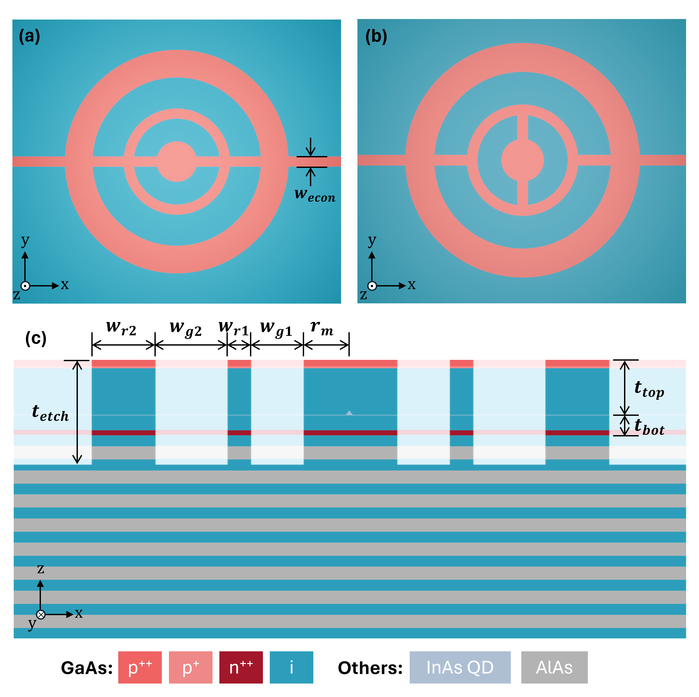
Designing a nanophotonic device involves careful consideration of the interplay between the geometry of individual structural elements in the proximity of the photon source (in this case, a QD) and their respective refractive indices. When modifying the well-known optically pumped CBG resonator concept into a ridge-based eCBG, the introduction of contact ridges which can lead to scattering and lateral photon losses is the primary factor influencing, and potentially reducing, the PEE. In this context, two aspects related to the electrical contacts are considered in particular: the electrical contact path length and the width of the ridge.
From the electrical perspective, the ridge should ideally have the shortest path length connecting the central mesa to the external areas to minimize the electrical resistance. This condition constitutes our first proposed design featuring direct-ridge electrical connections, illustrated in Figure 1a. In this design, when considering the optical perspective, such a straight ridge could provide an undesired optical loss channel for emitted photons from the central mesa via waveguiding, thereby deteriorating the lateral confinement. In fact, as a countermeasure, labyrinth-like structures have been proposed, where the connections between rings were sectioned and rotated 25. As a comparative experimental case study, another design featuring mazy-ridge electrical connections to reduce the effect of lateral waveguides is also proposed here and depicted in Figure 1b. To keep the electrical path as short as possible, both designs feature only two rings, and in the mazy-ridge design, only the connections inside the first ring are rotated.
A similar trade-off scenario applies to the width of the ridge as well. For electrical purposes, the ridge width should ideally be as large as possible to minimize the resistance, but as the ridge becomes wider, it could support the propagation of waveguiding modes 27, 28, degrading the optical performance of the device. While the optical performance could be predicted and optimized via numerical simulations, the sensible prediction for the electrical behavior of nanoscale structures requires experimental insights, for instance, on the width of depleted layers at the etched surfaces. In fact, our eCBGs are patterned and fabricated utilizing inductively coupled plasma reactive-ion etching (ICP-RIE), which usually results in residual surface defects with deteriorated electrical conductivity 29. As a consequence, a functional ridge must be wide enough to accommodate an electrically active region, sided by defective surfaces. For this, the minimum ridge width was initially selected as 100 nm, and the maximum ridge width was intuitively limited by the effective wavelength of typical InGaAs QD emissions (>900 nm) in GaAs medium, which is about 250 nm.
Based on the considerations mentioned above, numerical optimizations were performed to identify the optimal device parameters depicted in Figure 1c, by applying a Bayesian optimization algorithm to maximize the PEE at the numerical aperture (NA) of 0.81, which is the NA of the optics later used in the experiments. The field distributions and PEE were calculated by a three-dimensional (3D) finite-element method (FEM) in JCMsuite 30 based on the direct-ridge configuration, exploiting two vertical mirror planes (one along the main ridge axis and one perpendicular to it) to reduce the demanding computational time and resources for full 3D simulations. To sensibly limit the computation time for optimizations, the overall size of the simulated structures was bound by setting search ranges for the mesa radius (), ring widths (), gap widths (), and top/bottom-spacer () within 100 and 500 nm. The QD was modeled using two point-like dipoles oriented along the x- and y-axis emitting at the wavelength of 930 nm, and the absorption effect of dopants in p- and n-doped GaAs was neglected in the simulation at this wavelength.
| Structure | Device parameters [nm] | Sim. PEE [%] | ||||
|---|---|---|---|---|---|---|
| Direct-ridge | 100 | 243 | 268, 369 | 120, 327 | 630 | 43.2 |
| Mazy-ridge | 100 | 243 | 268, 369 | 120, 327 | 630 | 42.1 |
The device parameters obtained from the numerical optimization and the calculated PEEs for both designs are listed in Table 1. In this device design, the top spacer () and bottom spacer (), which distance the QDs from the surface and the DBR, were determined to be 333 nm and 119 nm, respectively. The uppermost part of the top spacer was chosen as a 50 nm p-doped layer, while the lowermost part of the bottom spacer was chosen as a 30 nm n-doped layer. It is important to point out that the optimal value for the highest PEE was found at the lower boundary of the defined search domain, which was 100 nm, implying a narrow ridge width was favored. This numerical study, which predicts PEEs of 43.2% and 42.1% for the two considered eCBG configurations, confirmed the assumptions mentioned earlier regarding the ridge width and implied that the main limiting criterion for a functional ridge width is the electrical conductivity which needed to be investigated experimentally.
2.2 Deterministic Fabrication
Following the aforementioned optimized design parameters, the heterostructure was epitaxially grown using MBE as follows. Firstly, at a substrate temperature of 605 °C, a 100 nm GaAs buffer layer was deposited on an undoped GaAs (100) wafer, followed by the growth of a DBR consisting of ten pairs of AlAs and GaAs layers with nominal thicknesses of 79 nm and 67 nm, respectively. Subsequently, a 30 nm Si-doped GaAs layer with a doping concentration of cm-3 was grown at 555 °C. Then, the substrate temperature was returned to 605 °C, and an 86 nm GaAs layer was deposited. Afterward, a 3-minute pause was introduced during which the substrate temperature was lowered from 605 °C to 505 °C, and the arsenic pressure was gradually reduced from mbar to mbar. After a 2-minute temperature stabilization period, 3 nm of GaAs were deposited. Indium was then deposited in a pulsed mode (4 s deposition, 4 s pause) over 20.5 deposition cycles. During the initial 10.5 cycles, the substrate rotation was halted to create an indium gradient along the [110] direction. The rotation was resumed for the remaining 10 cycles at a speed of 10 rpm. The QDs were then partially capped with 2.6 nm of GaAs at 485 °C. Following this, the temperature was rapidly increased to 60 5°C, and a 280 nm GaAs layer was grown. Lastly, a top gate structure consisting of 10 nm and 40 nm C-doped GaAs layers, with doping concentrations of cm-3 and cm-3, respectively, was deposited at 555 °C. All temperatures mentioned were determined using band-edge thermometry.
Following the epitaxial growth, a sample piece of (55) mm2 with low QD density (about cm-2) was selected, on which electrical contacts and \chAu markers were prepared via four EBL steps. The first lithography was performed to pattern areas at the sample corners, which were then etched by 410 nm using ICP-RIE to remove the top p-doped layer and prepare for n-pads. Then, within the etched areas, n-contact pads were patterned and deposited with thicknesses of 10 nm \chNi, 50 nm Au0.88Ge0.12, and 40 nm Au. After that, the sample was rapidly annealed at 420 °C for 90 s with a 500 K/min ramping rate under \chN2 atmosphere. For the third EBL, p-contacts and markers were patterned, and 10 nm \chTi and 90 nm \chAu were deposited. Lastly, all p- and n-contacts were deposited with an additional 250 nm \chAu, to achieve the total pad thickness of 350 nm to ensure the durability of the pads during the wire bonding procedure.
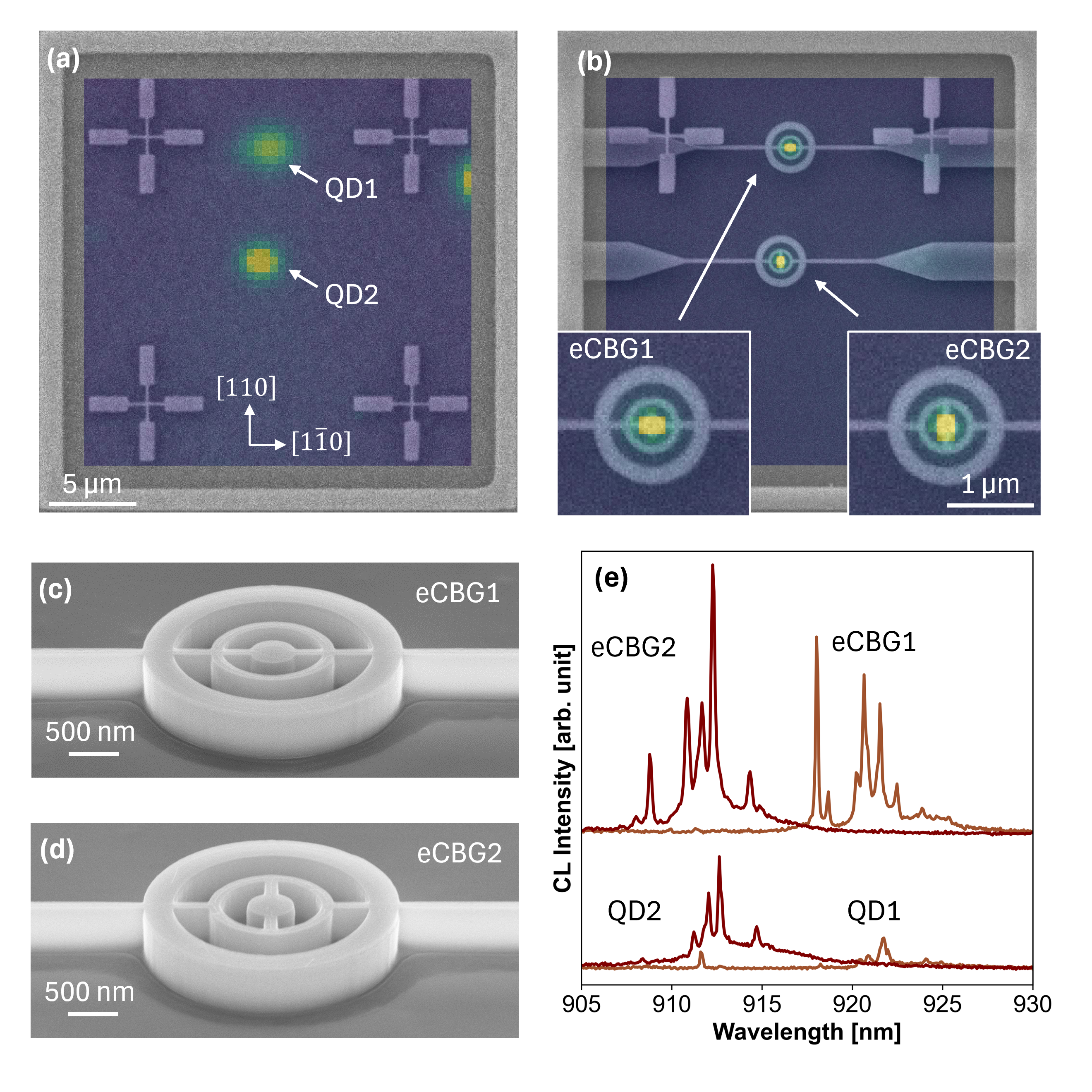
Suitable QDs were identified based on their emission wavelength and separation from other QDs on the sample with pre-patterned markers by scanning each marker field using CL mapping at 20 K without applying any bias voltage (open-circuit). A map consisting of an array of CL spectra and a scanning electron microscope (SEM) image, as illustrated using an exemplary field in Figure 2a, provides spectral and spatial information about suitable QDs, which can be pre-selected for device fabrication. After identifying the QDs, marker-based EBL 31 and ICP-RIE were performed to pattern eCBGs at the determined QD positions. As the definitive minimum ridge width for an electrically active eCBG was unknown, the ridge width was intentionally varied from 100 to 130 nm on different patterned structures without changing any other parameters.
The enhancement from the eCBG integration on the QDs could be observed via a one-to-one comparison by performing another CL mapping on the same marker field after the integration, as depicted in Figure 2b, showing that devices were patterned on the determined QDs. Note that the QD emission spectra could be observed on all 14 patterned devices regardless of their patterned ridge widths as they were visible in open-circuit states. In the marker field, two QDs (namely QD1 and QD2) were integrated into a direct-ridge structure (eCBG1) and a mazy-ridge structure (eCBG2) whose SEM images are illustrated in Figure 2c and d, respectively. The images indicate smooth etched surfaces and well-defined fabrication conditions. Figure 2e shows the CL spectra of both QDs before and after device integration using the same excitation and collection parameters. It is important to note that the intensity between QDs could not be compared fairly as the CL mapping was performed using a parabolic mirror, which resulted in a non-uniform intensity profile throughout the map. Qualitatively, the post-integration spectra of both QDs clearly indicate strongly enhanced extraction efficiency and improved signal-to-noise ratio.
2.3 Electric-field Dependent Photoluminescence Measurements
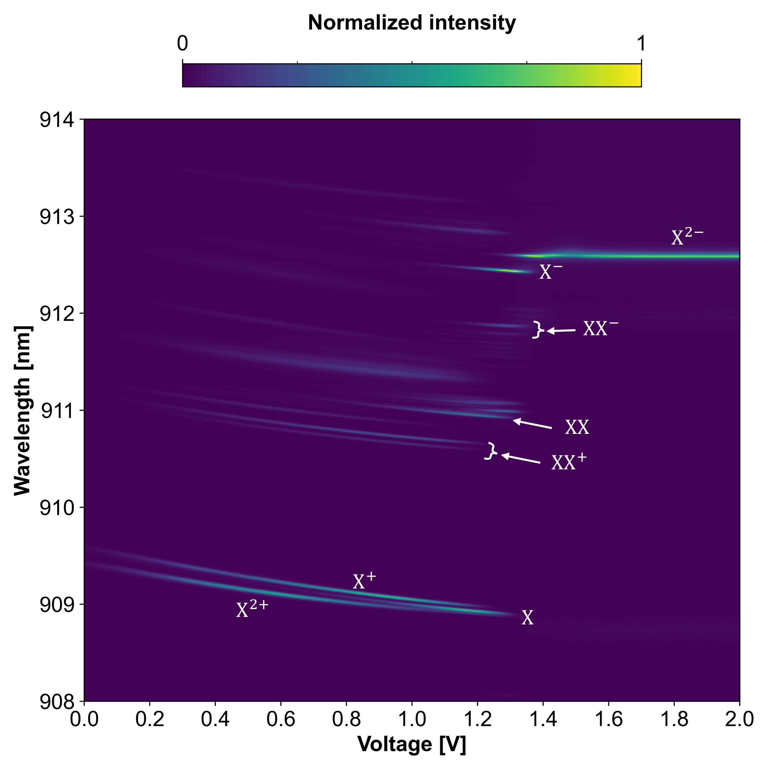
After the deterministic fabrication, electrical connections between an external voltage source and the diode structures of the fabricated devices were made through wire bonding between a chip carrier and deposited metallic contact pads. The chip carrier was then installed in the optical setup described in Section 4.1 for bias-voltage dependent PL measurements. The eCBGs were investigated under pulsed (80 MHz) ps-mode excitation via wetting layer at 865 nm using a Ti:Sapphire laser. By varying the external bias voltage () between 0 and 3 V, we observed that the fabricated direct-ridge eCBGs whose ridges were narrower than (1105) nm exhibited no voltage dependency on their optical spectra, as well as the mazy-ridge eCBGs whose ridges were narrower than (1205) nm. Both eCBG1 and eCBG2, as well as other eCBGs that consisted of wider ridges than these values, showed clear and similar bias-voltage dependency, as illustrated using eCBG2 as an example in Figure 3.
The PL contour plot displays different QD emission lines observed at different . Most lines, which appeared below about 1.4 V, featured the quantum-confined Stark effect by which the emission wavelengths shifted gradually over the change, whereas the emission lines appearing above 1.4 V remained energetically constant. This behavior can be explained by the electronic band-bending of the PIN diode structure, which was initially caused by the built-in electric field () 14. At zero bias, the electronic bands were strongly bent by the field which promotes the quantum tunneling rate of electrons from the wetting layer to GaAs, reducing carrier capturing into the QD, hence, the low PL emission rates were observed at 0 V 32, 33. As the increased, the band-bending and electron tunneling weakened, enabling the carrier capturing in the QD and subsequent carrier recombination, hence the emission lines became visible while shifting energetically 33, 15. Notably, bias-induced energetic shifts of up to 0.7 meV were observed in the studied devices. When the externally applied electric field became as equally strong as the , which was at around = 1.4 V), flat-band conditions were achieved, and no quantum confined Stark tuning could be observed anymore.
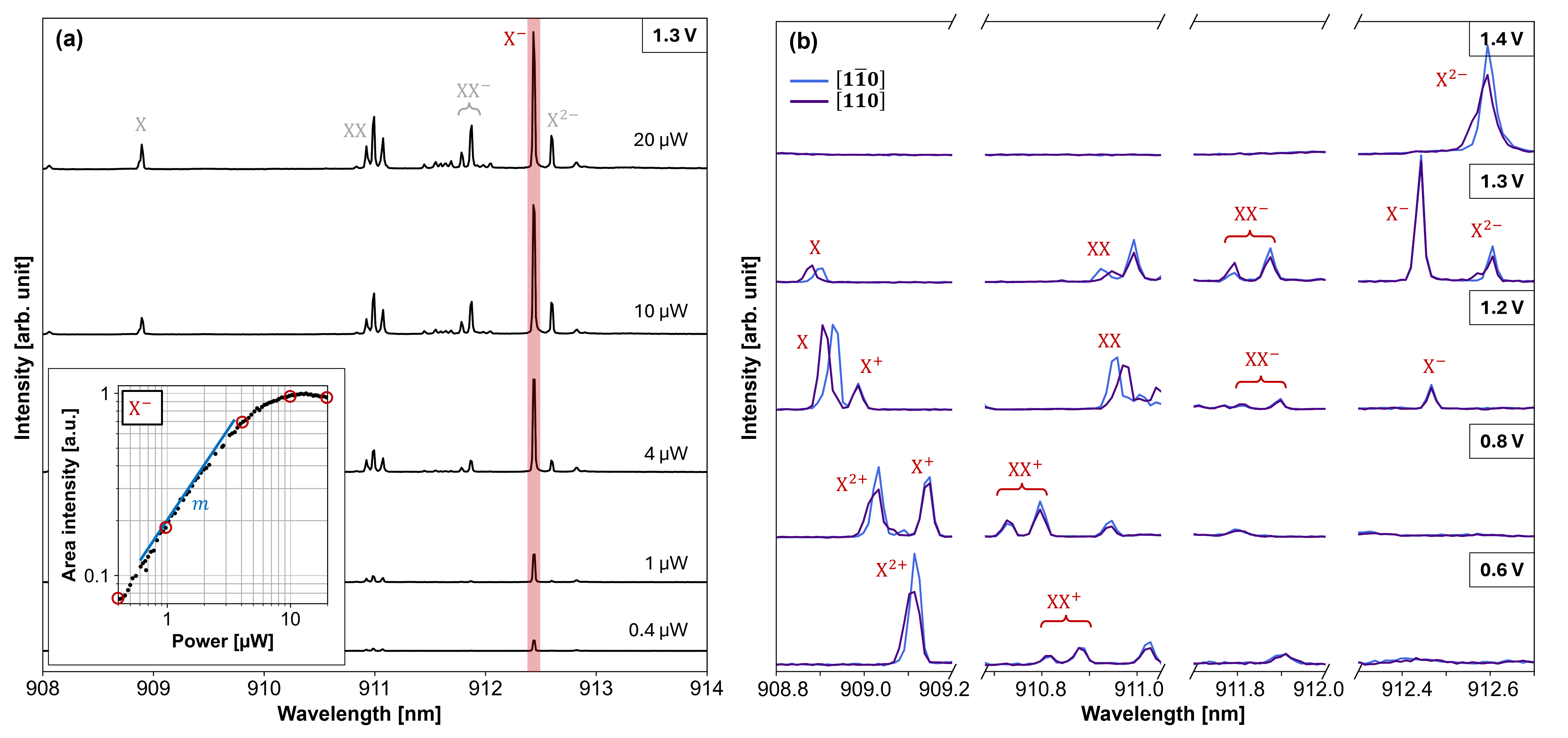
The nature of observed emission lines was determined by performing power- and polarization-dependent PL measurements at the corresponding . For the power-dependent measurements, the PL spectra were recorded at different optical excitation power. By selectively fitting the area intensity of each emission line and plotting them against the excitation power in a log-log scale, a power exponent () can be extracted from the slope of the linear section in the plot. Figure 4a shows an example of a power-dependent PL measurement at 1.3 V where an emission line (later determined as the emission line) was selectively fitted. The same process was done for other lines and the findings are listed in Table 2. With extracted ’s, excitonic and biexcitonic lines were categorized by their linear () and superlinear (>1) power dependencies, respectively 34. Complementarily, the information on polarization properties of these emission lines was necessary to determine their origins unambiguously, caused by the spin-related fine structures 35, 36, 37. For this, the polarization-dependent measurements were performed by inserting a rotatable -plate and a linear polarizer in the collection path of the PL setup. By changing the -plate angle, different polarization components of each emission line were recorded. Figure 4b shows the two polarization components of each emission line along and [110] orientations of the sample. For each line, the peak energy difference between the two polarization angles and the linewidth (full-width half-maximum measured at a certain polarization angle where the narrowest emission was observed) were determined and are also listed in Table 2. Combining the findings from these two measurements, the emission lines were determined as follows.
| Emission | Voltage [V] | [nm] | E [meV] | E [eV] | FWHM [eV] | |
|---|---|---|---|---|---|---|
| 0.6 | 909.11 | 1366.58 | 1.51±0.01 | 9.0±1.8 | 31.5±2.9 | |
| 0.8 | 909.14 | 1366.53 | 0.85±0.01 | None | 23.7±2.5 | |
| 0.8 | 910.73 | 1364.15 | 1.50±0.02 | None | 24.8±4.6 | |
| 0.8 | 910.80 | 1364.05 | 1.60±0.03 | None | 29.7±3.1 | |
| X | 1.2 | 908.92 | 1366.87 | 0.82±0.01 | 37.2±2.6 | 24.6±4.7 |
| XX | 1.2 | 910.96 | 1363.81 | 1.28±0.01 | 34.4±2.4 | 27.2±2.4 |
| 1.3 | 911.79 | 1362.57 | 1.69±0.04 | None | 28.9±3.1 | |
| 1.3 | 911.87 | 1362.44 | 1.78±0.02 | None | 29.4±1.2 | |
| 1.3 | 912.44 | 1361.60 | 0.97±0.01 | None | 16.6±1.1 | |
| 1.4 | 912.59 | 1361.37 | 1.29±0.01 | 7.7±1.4 | 46.0±1.2 |
Firstly, the most fundamental states of QD, exciton-biexciton (X-XX) emissions were observed at around 1.2 V exhibiting a strong polarization dependency with the opposite energetic deviation direction. The energy deviations indicate the X-XX fine-structure splittings of (37.22.6) for X and (34.42.4) eV for XX, respectively, which are typical values for an InGaAs QD 38. Secondly, when varying slightly to a lower value (0.8 V), three prominent lines were observed without any polarization-dependent energetic variation, consisting of a single line with and double lines with . This suggests that they originate from singly-charged excitonic and biexcitonic states. Moreover, the double lines exhibited clear polarization-dependent intensities, where each line was more prominent than the other at different polarization angles. This strongly supports that they originate from the relaxation of the charged biexcitonic state into the two triplet states of excited-trion, which typically generate elliptically-polarized photons 35, 39. Thirdly, when decreasing even further (<0.8 V), a new prominent line appeared having and showing a polarization-dependent emission. The emission was observed as a single line at a certain polarization angle, but the line broadened with a lower peak intensity when observed at different polarization angles. This suggests that the emission consists of two different lines, one without polarization dependency and another with polarization-dependent energetic variation, which could be attributed to the two triplet transitions from doubly-charged excitonic states 40, 36.
Another similar set of lines was observed as well when varying the voltage to the higher values (>1.2 V), indicating that they originate from the analogous spin states with the opposite charge sign. Note that, at lower voltages (<1.2 V) where the band-bending exists, the tunneling rate of electrons is more significantly promoted than that of holes, due to the smaller effective mass, suggesting the hole is more effectively captured into the QD and the prominent emission lines are expected to originate from the positively charged states 32, 33. On the other hand, at higher voltages (>1.2 V) where the tunneling weakens, the electron capturing in the QD becomes effective, suggesting that the emission lines in this regime originate from negatively charged states instead. Additionally, the redshifts of the higher negatively-charged emission lines also support the assumptions, in agreement with previously reported studies 40, 41, 42. Consequently, all the prominent emission lines in the voltage-dependent PL spectra were assigned, ranging from the positive doubly-charged line () at low voltages to the negative doubly-charged line () at high voltages, as shown in Figure 3.
Understanding the spin-related origins of the emission lines is crucial for application in, for instance, quantum repeater networks, which require well-defined light-matter interactions between the flying and stationary qubits 6. The results presented in this section demonstrate the determination of the origins of multiple QD emission lines and confirm the capability of the designed eCBG devices, allowing for deterministic controls of electronic states of QDs in the cavity. This feature can significantly enhance the performance of spin-photon interfaces, crucial for mediating photon entanglements in quantum repeater networks 43. The emission wavelength tunability of the QD in the cavity enabled by this design can also benefit the applications with quantum memories 44. Moreover, the design can be directly applied to QD molecules, which have promising applications in photonic cluster-state generation 45, 13, 46, 47.
2.4 Optical Enhancements
| Structure | Device parameters [nm] | PEE [%] | [nm] | |||||
|---|---|---|---|---|---|---|---|---|
| Simulated | Measured | |||||||
| Planar | - | - | - | - | 0 | 2.020.19 | 1.690.59 | 900 – 930 |
| eCBG1 | 122 | 240 | 250, 368 | 137, 324 | 633 | 24.53 | 12.61.4 | 918.1 |
| eCBG2 | 132 | 245 | 240, 368 | 137, 328 | 633 | 31.93 | 30.43.4 | 912.7 |
As mentioned in the previous section, the electrically functioning eCBGs were experimentally found to require wider ridges than the originally optimized value (100 nm). For a fair comparison between the simulation and experimental results, the actual geometry of the fabricated structures (eCBG1 and eCBG2) was measured using SEM, and the PEEs were re-simulated based on the measured structural parameters which are listed in Table 3. Note that the experimental PEE can deviate from the simulated value due to the possible mismatch of the QD position and the integrated eCBG 48, which could not be determined in this work, limited by the small diameter of the central mesa.
To obtain experimental PEEs, the PL setup efficiency was measured using a continuous-wave laser at the same wavelength as the QD emission, yielding the value of (7.30.8)%. Then, nine different QDs in the planar structure and the studied devices (eCBG1 and eCBG2) were electrically biased at 1.5 V to achieve the flat-band conditions for maximum electric-field dependent PL emissions 32, and the emission spectrum from each QD was recorded under pulsed (80 MHz) excitation at 800 nm using a Ti:Sapphire laser with the corresponding saturation optical pump power. The PEE was calculated using the formula:
where is the single-photon emission rate, is the setup efficiency, and is the excitation frequency. For eCBG1 and eCBG2, single-photon emission rates were measured to be (73218) kHz and (1.770.34) MHz, equivalent to PEEs of (12.61.4)%. and (30.43.4)%, respectively. For planar QDs, the average (and standard deviation) emission rate was found to be (98.626.1) kHz, which led to an average PEE of (1.690.59)%.
The comparison between the simulated and experimental PEE for eCBG2 shows impressive conformity, indicating accurate numerical modeling and good fabrication quality. The reliability of this comparison can be supported by the results from planar QDs, which also show good agreement between the simulation and the measured value. Deviated from the simulation, eCBG1 yielded noticeably lower efficiency, similar to the other two fabricated direct-ridge eCBGs with the same nominal parameters. The cause for the larger deviation of the experimental PEE from the simulated one for eCBG1 than that of eCBG2 may be multi-factored. Firstly, although all eCBGs were fabricated under identical conditions, since the actual eCBG-to-QD position offsets could not be determined, the effect of alignment mismatch cannot be completely ruled out. Secondly, the simulations were performed with a QD modeled as two equally contributing perpendicular point-like dipoles, which might not represent the actual QD emission well enough in the presence of ridge-like structures breaking the cylindrical symmetry. As a result, the simulation may have underestimated the undesired direct-ridge effect, causing a larger difference between simulated and experimental PEEs only for direct-ridge eCBGs. An additional finding described as follows supports this assumption further.
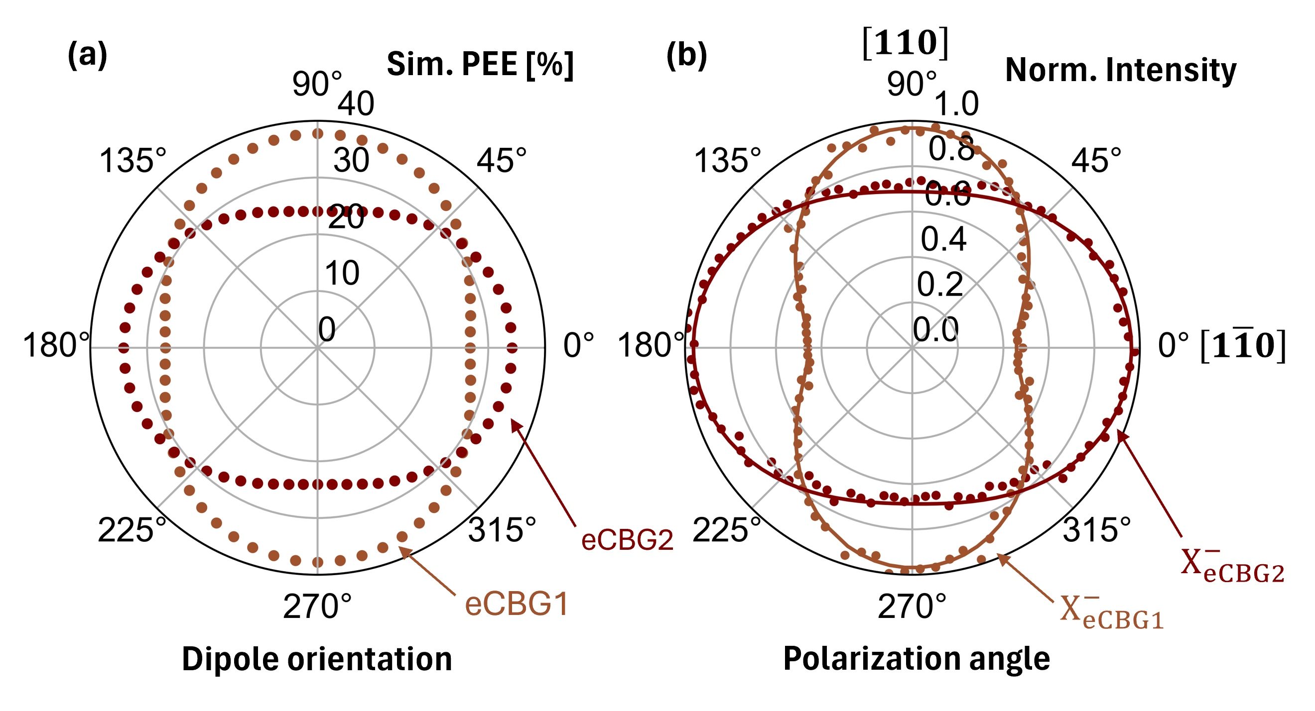
Due to the presence of the ridges in eCBGs, the polarization-dependent optical performance of the fabricated devices was intuitively anticipated. On the simulation side, the effect was predicted by calculating the PEE using a single in-plane dipole oriented at different angles related to the main ridge axis. The simulation results for eCBG1 and eCBG2, plotted in Figure 5a, illustrate good enhancements for the dipoles oscillating perpendicularly to the innermost ridge axis, whereas the enhancements deteriorated the most when the dipole was placed in parallel instead. The simulated PEEs could be normalized and calculated into a degree of linear polarization: , where are maximum and minimum intensity (equivalent to PEE). Interestingly, both eCBG1 and eCBG2 yielded the same simulated DLP of 17%, regardless of the difference in the ridge continuity. On the experimental side, the effect could be observed in polarization-dependent PL measurements mentioned in the previous section. To exemplify the effect, the emission line (912.44 nm) which is intrinsically circularly polarized was selected, and the fitted polarization-dependent intensity plots are shown in Figure 5b. Note that the polarization angle of 0° corresponded to the polarization components along the orientation of the sample, to which the main ridge axes of the fabricated devices were aligned. Qualitatively, the experimental plots closely match the simulation results well, clearly confirming the polarization-dependency of PEEs. The experimental DLPs were calculated in the same fashion as earlier, yielding (361)% and (171)% for eCBG1 and eCBG2, respectively. For eCBG1, the experimental result implies poorer enhancement of the emission along the main ridge axis than the simulation predicted, which was another piece of evidence signifying the underestimation of the direct-ridge effect on the optical enhancement of the eCBG. On the other hand, another perfect match between simulation and experimental results on eCBG2 could be observed for DLP values. Thus, we conclude that this polarization-dependency of PEEs is mostly affected by the innermost ridges, which suggests that the outer ridges can be modified (e.g. for larger widths) to support electrical conductivity without significantly degrading the optical property.
| Structure | Device parameters [nm] | Sim. PEE [%] | ||||
|---|---|---|---|---|---|---|
| Direct-ridge | 120 | 256 | 960, 607 | 257, 628 | 630 | 55.65 |
| Mazy-ridge | 120 | 256 | 960, 607 | 257, 628 | 630 | 56.54 |
To demonstrate the capability of improving the current designs, another numerical optimization was performed by setting to 120 nm and expanding the parameter search ranges for ring and gap widths up to 1000 nm. The newly optimized parameters yielded the PEE > 50%, listed in Table 4, promising a substantial improvement without changing the heterostructure parameters. With numerical refinement, the proposed design can be adapted with more pairs of back-side DBR to boost the PEE even further.
2.5 Single-photon Characteristics
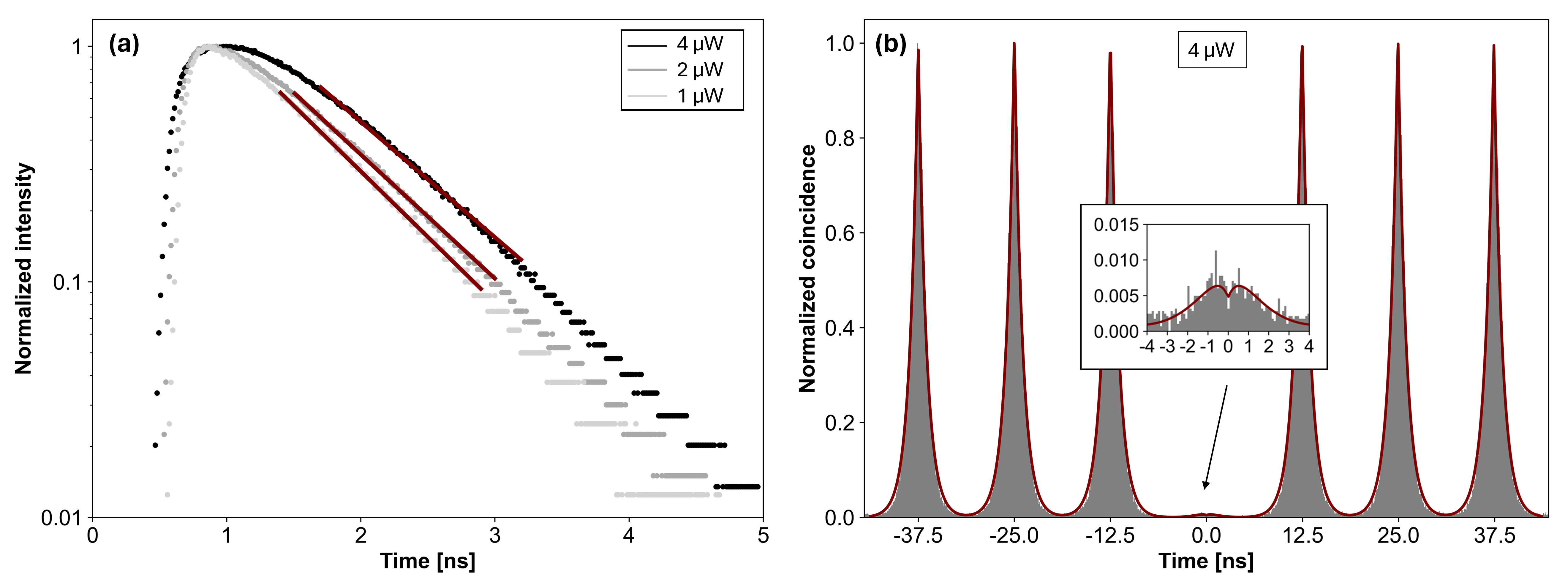
In addition to the optical performance of the fabricated devices, the quantum optical properties were also assessed by performing time-resolved PL measurements. For this, the emission line (912.44 nm) from eCBG2 was selected, as it appeared near the flat-band condition, resulting in a bright emission and a resolution-limited linewidth of (16.61.1) eV. The experiment was conducted under pulsed (80 MHz) ps-mode excitation at 865 nm using a Ti:Sapphire laser, and the detection path included a monochromator as a spectral filter and a photon correlation setup equipped with superconducting nanowire single-photon detectors (SNSPDs). Firstly, the time-resolved PL measurements were performed under different excitation powers, and the results are illustrated in Figure 6. Note that excitation powers of 1, 2, and 4 W corresponded to the emissions with 20, 40, and 70 of the saturation intensity, respectively, as previously shown in Figure 4a. The emission lifetimes were found to increase gradually from (0.780.01) to (0.890.01) ns, as the power increased from 1 to 4 W. For further measurements, the excitation power of 4 W was applied to maximize the emission rate.
Following the lifetime measurements, a Hanbury Brown and Twiss (HBT) setup 49 was used to assess the single-photon purity. The recorded photon correlation histogram, plotted in Figure 6, shows a very low coincidence rate observed near the zero-time delay, which can be expected from carrier-recapturing processes due to the non-resonant excitation scheme. Nevertheless, the emission features an excellent multi-photon suppression rate with a of (1.20.2)% and a post-selected of (0.50.3)%, which are equivalent to the non-post-selected and post-selected single-photon purities of (98.80.2)% and (99.50.3)%, respectively. Notably, the multi-photon suppression rate can be further improved by either reducing the excitation power, at the cost of a lower emission rate or by operating the device under resonant excitation 50.
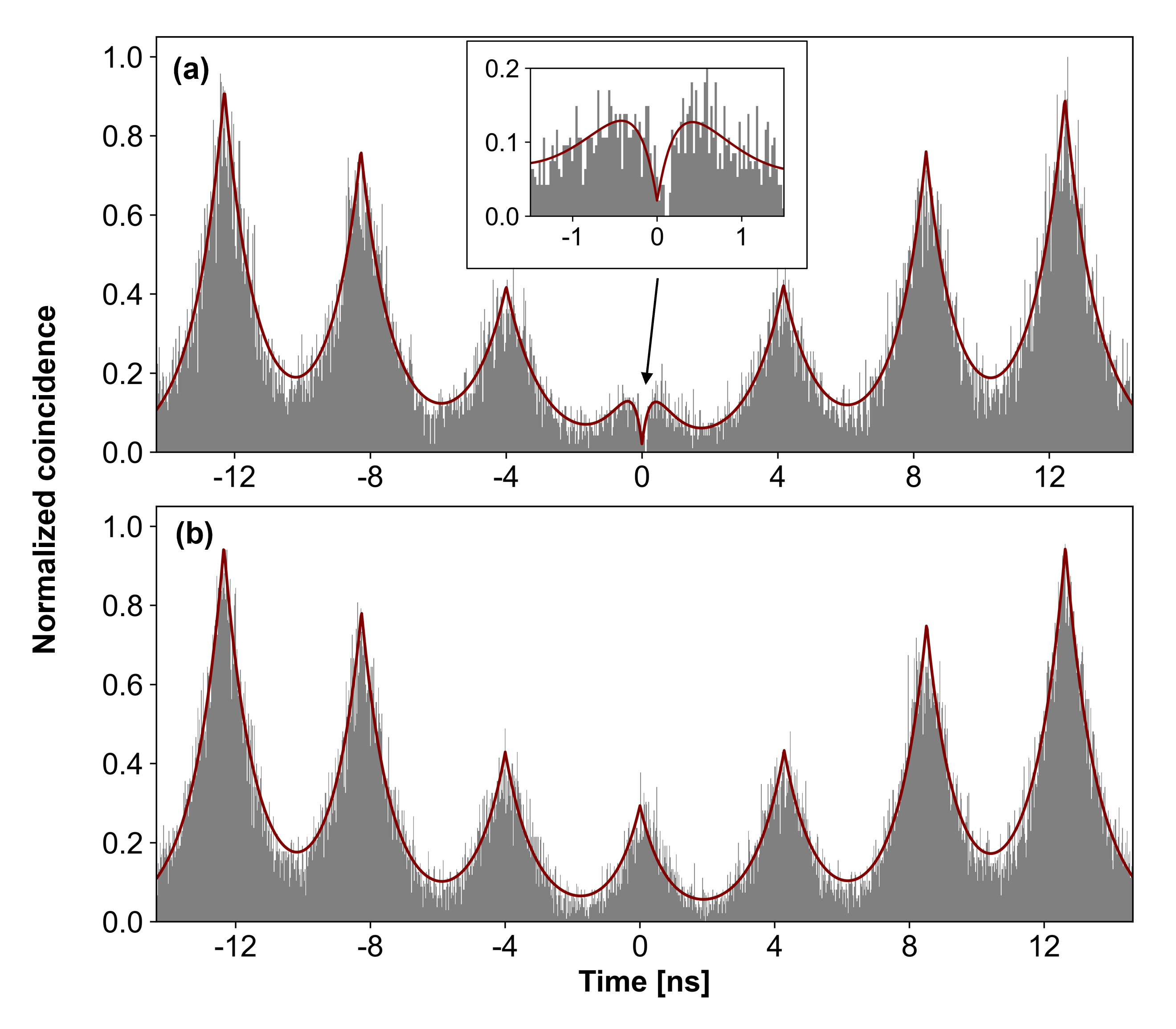
After determining the single-photon purity, the photon indistinguishability was assessed using a Hong-Ou-Mandel (HOM) correlation setup 51. In this case, a sequence of double excitation pulses with a 4 ns pulse separation was used, which was matched with a 4 ns fiber delay line in one interferometer arm in the HOM setup. The HOM interference histograms from parallel and orthogonal polarization configurations are plotted in Figure 7. The non-ideal raw visibility was obtained as = (25.82.1)%, evidenced by observed coincidences near the zero-time delay. These coincidences were observed, potentially because the QD had a non-enhanced recombination lifetime allowing the carriers to interact with the solid-state environment, and due to spectral diffusion induced by charge fluctuations at the etched surface near the QD 52. However, prominent indistinguishability could be observed at zero-time delay in the parallel polarization configuration, leading to the post-selected visibility = (92.84.8)%. This indicates that QD could intrinsically emit indistinguishable photons, suggesting that optimizing the design toward Purcell enhancement, as well as operating the device under resonant excitation and applying surface passivation, could improve the raw visibility of the device further.
3 Conclusion
In this report, we proposed and implemented an innovative concept for high-performance electrically controlled QD-CBG single-photon sources. By going beyond simple optically controlled structures, our work can To maximize the brightness of the quantum devices we explored two different ridge-based eCBG designs, based on the trade-off between electrical and optical performance. The sensitivity of the electrical path length and the ridge width to the performance prompted careful optimizations between numerical and experimental results. A direct-ridge configuration featured better electrical connection, requiring a slightly narrower minimum ridge width for an electrically functioning device, while optically performing poorer, especially for the polarization in parallel to the ridge axis. On the other hand, a mazy-ridge configuration featured a slightly longer electrical path length, requiring a wider minimum ridge width to function, but yielded superior optical enhancement. The determinsitically fabricated mazy-ridge eCBG-QD achieved a PEE of (30.4±3.4)%, in quantitative agreement with numerical simulations which promise substantial improvement with PEE >50 % when using re-optimized parameters based on the present experiment findings. The electrical operation of the eCBG-QD yields precise charge control and a quantum-confined Stark effect, providing robust capability to fine-tune the emission wavelength up to 0.7 nm and selectively enhance emission lines from specific QD states. The single-photon emission characteristics show impressive a single-photon purity of (98.8±0.2)% and post-selected visibility of (92.8±4.8)%. The results underscore the high potential of our advanced quantum device concept, which can pave the way for many applications of photonic quantum information technology requiring not only excellent optical and quantum optical properties but also tight electrical control of the integrated quantum emitters.
4 Experimental methods
4.1 Optical Setups
The PL measurements were performed on the sample cooled to 4 K in a closed-cycle cryostat using a Ti:Sapphire laser operating in pulsed ps-mode (80 MHz) at tunable wavelengths (800-865 nm). The emitted photons were collected with a cold aspheric objective lens (NA = 0.81). With a beam splitter, which separates excitation and collection paths, the collected beam was directed through a 900 nm long-pass filter to a monochromator with a 1500-line-per-nm grating and detected using a CCD camera. For time-resolved measurements, two different correlation setups, equipped with SNSPDs, were used: (1) HBT setup, where the spectrally filtered photons were sent through a 1:1 single-mode fiber beam splitter and detected with two SNSPDs were recorded, and (2) Hong-Ou-Mandel setup, where the spectrally filtered photons were sent through a polarization-maintaining beam splitter in combination with polarization-control paths (with and plates) and a 4 ns time delay on one arm, before sent back into a 1:1 beam splitter for two-photon interference effect and detected with two SNSPDs. In these correlation setups, the time correlation between two detected photons in each detector was recorded.
This work was financially supported by the German Federal Ministry of Education and Research (BMBF) through the project “QR.X – Quantenrepeater.Link” with funding IDs: 16KISQ012 and 16KISQ014. The authors further thank Johannes Schall, Ching-Wen Shih, Chirag Palekar, Lucas Rickert, Niels Heermeier, and Aris Koulas-Simos for technical support and guidance.
The data that support the findings of this study are available from the corresponding author upon a reasonable request.
References
- Briegel et al. 1998 Briegel, H.-J.; Dür, W.; Cirac, J. I.; Zoller, P. Quantum Repeaters: The Role of Imperfect Local Operations in Quantum Communication. Physical Review Letters 1998, 81, 5932–5935
- Sangouard et al. 2007 Sangouard, N.; Simon, C.; Minář, J.; Zbinden, H.; de Riedmatten, H.; Gisin, N. Long-distance entanglement distribution with single-photon sources. Physical Review A 2007, 76, 050301
- Lu and Pan 2014 Lu, C.-Y.; Pan, J.-W. Push-button photon entanglement. Nature Photonics 2014, 8, 174–176
- Wang et al. 2019 Wang, H. et al. On-Demand Semiconductor Source of Entangled Photons Which Simultaneously Has High Fidelity, Efficiency, and Indistinguishability. Physical Review Letters 2019, 122, 113602
- Aharonovich et al. 2016 Aharonovich, I.; Englund, D.; Toth, M. Solid-state single-photon emitters. Nature Photonics 2016, 10, 631–641
- Heindel et al. 2023 Heindel, T.; Kim, J.-H.; Gregersen, N.; Rastelli, A.; Reitzenstein, S. Quantum dots for photonic quantum information technology. Advances in Optics and Photonics 2023, 15, 613
- Rodt et al. 2020 Rodt, S.; Reitzenstein, S.; Heindel, T. Deterministically fabricated solid-state quantum-light sources. Journal of Physics: Condensed Matter 2020, 32, 153003
- Patel et al. 2010 Patel, R. B.; Bennett, A. J.; Farrer, I.; Nicoll, C. A.; Ritchie, D. A.; Shields, A. J. Two-photon interference of the emission from electrically tunable remote quantum dots. Nature Photonics 2010, 4, 632–635
- Zhai et al. 2022 Zhai, L.; Nguyen, G. N.; Spinnler, C.; Ritzmann, J.; Löbl, M. C.; Wieck, A. D.; Ludwig, A.; Javadi, A.; Warburton, R. J. Quantum Interference of Identical Photons from Remote GaAs Quantum Dots. Nature Nanotechnology 2022, 17, 829–833, arXiv:2106.03871 [cond-mat, physics:quant-ph]
- Warburton et al. 1997 Warburton, R. J.; Dürr, C. S.; Karrai, K.; Kotthaus, J. P.; Medeiros-Ribeiro, G.; Petroff, P. M. Charged Excitons in Self-Assembled Semiconductor Quantum Dots. Physical Review Letters 1997, 79, 5282–5285
- Hermannstädter et al. 2009 Hermannstädter, C.; Witzany, M.; Beirne, G. J.; Schulz, W.-M.; Eichfelder, M.; Rossbach, R.; Jetter, M.; Michler, P.; Wang, L.; Rastelli, A.; Schmidt, O. G. Polarization fine structure and enhanced single-photon emission of self-assembled lateral InGaAs quantum dot molecules embedded in a planar microcavity. Journal of Applied Physics 2009, 105, 122408
- Löbl et al. 2017 Löbl, M. C.; Söllner, I.; Javadi, A.; Pregnolato, T.; Schott, R.; Midolo, L.; Kuhlmann, A. V.; Stobbe, S.; Wieck, A. D.; Lodahl, P.; Ludwig, A.; Warburton, R. J. Narrow optical linewidths and spin pumping on charge-tunable close-to-surface self-assembled quantum dots in an ultrathin diode. Physical Review B 2017, 96, 165440
- Schall et al. 2021 Schall, J. et al. Bright Electrically Controllable Quantum-Dot-Molecule Devices Fabricated by In Situ Electron-Beam Lithography. Advanced Quantum Technologies 2021, 4, 2100002
- Miller et al. 1984 Miller, D. A. B.; Chemla, D. S.; Damen, T. C.; Gossard, A. C.; Wiegmann, W.; Wood, T. H.; Burrus, C. A. Band-Edge Electroabsorption in Quantum Well Structures: The Quantum-Confined Stark Effect. Physical Review Letters 1984, 53, 2173–2176
- Bennett et al. 2010 Bennett, A. J.; Patel, R. B.; Skiba-Szymanska, J.; Nicoll, C. A.; Farrer, I.; Ritchie, D. A.; Shields, A. J. Giant Stark effect in the emission of single semiconductor quantum dots. Applied Physics Letters 2010, 97, 031104
- Nowak et al. 2014 Nowak, A. K.; Portalupi, S. L.; Giesz, V.; Gazzano, O.; Dal Savio, C.; Braun, P.-F.; Karrai, K.; Arnold, C.; Lanco, L.; Sagnes, I.; Lemaître, A.; Senellart, P. Deterministic and electrically tunable bright single-photon source. Nature Communications 2014, 5, 3240
- Schnauber et al. 2021 Schnauber, P.; Große, J.; Kaganskiy, A.; Ott, M.; Anikin, P.; Schmidt, R.; Rodt, S.; Reitzenstein, S. Spectral control of deterministically fabricated quantum dot waveguide systems using the quantum confined Stark effect. APL Photonics 2021, 6, 050801
- Davanço et al. 2011 Davanço, M.; Rakher, M. T.; Schuh, D.; Badolato, A.; Srinivasan, K. A circular dielectric grating for vertical extraction of single quantum dot emission. Applied Physics Letters 2011, 99, 041102
- Liu et al. 2019 Liu, J.; Su, R.; Wei, Y.; Yao, B.; Silva, S. F. C. D.; Yu, Y.; Iles-Smith, J.; Srinivasan, K.; Rastelli, A.; Li, J.; Wang, X. A solid-state source of strongly entangled photon pairs with high brightness and indistinguishability. Nature Nanotechnology 2019, 14, 586–593
- Ates et al. 2012 Ates, S.; Sapienza, L.; Davanco, M.; Badolato, A.; Srinivasan, K. Bright Single-Photon Emission From a Quantum Dot in a Circular Bragg Grating Microcavity. IEEE Journal of Selected Topics in Quantum Electronics 2012, 18, 1711–1721
- Yao et al. 2018 Yao, B.; Su, R.; Wei, Y.; Liu, Z.; Zhao, T.; Liu, J. Design for Hybrid Circular Bragg Gratings for a Highly Efficient Quantum-Dot Single-Photon Source. Journal of the Korean Physical Society 2018, 73, 1502–1505
- Rickert et al. 2023 Rickert, L.; Betz, F.; Plock, M.; Burger, S.; Heindel, T. High-performance designs for fiber-pigtailed quantum-light sources based on quantum dots in electrically-controlled circular Bragg gratings. Optics Express 2023, 31, 14750
- Ji et al. 2021 Ji, S.; Tajiri, T.; Kiyama, H.; Oiwa, A.; Iwamoto, S. Design of bull’s-eye optical cavity toward efficient quantum media conversion using gate-defined quantum dot. Japanese Journal of Applied Physics 2021, 60, 102003
- Barbiero et al. 2022 Barbiero, A.; Huwer, J.; Skiba-Szymanska, J.; Müller, T.; Stevenson, R. M.; Shields, A. J. Design study for an efficient semiconductor quantum light source operating in the telecom C-band based on an electrically-driven circular Bragg grating. Optics Express 2022, 30, 10919
- Buchinger et al. 2023 Buchinger, Q.; Betzold, S.; Höfling, S.; Huber-Loyola, T. Optical properties of circular Bragg gratings with labyrinth geometry to enable electrical contacts. Applied Physics Letters 2023, 122, 111110
- Shih et al. 2023 Shih, C.-W.; Rodt, S.; Reitzenstein, S. Universal design method for bright quantum light sources based on circular Bragg grating cavities. Optics Express 2023, 31, 35552
- Schnauber et al. 2019 Schnauber, P.; Singh, A.; Schall, J.; Park, S. I.; Song, J. D.; Rodt, S.; Srinivasan, K.; Reitzenstein, S.; Davanco, M. Indistinguishable Photons from Deterministically Integrated Single Quantum Dots in Heterogeneous GaAs/Si N Quantum Photonic Circuits. Nano Letters 2019, 19, 7164–7172
- Hoehne et al. 2019 Hoehne, T.; Schnauber, P.; Rodt, S.; Reitzenstein, S.; Burger, S. Numerical Investigation of Light Emission from Quantum Dots Embedded into On-Chip, Low-Index-Contrast Optical Waveguides. physica status solidi (b) 2019, 256, 1800437
- Cole et al. 1992 Cole, M. W.; Salimian, S.; Cooper, C. B.; Lee, H. S.; Dutta, M. Reactive ion etching of GaAs with SiCl : A residual damage and electrical investigation. Scanning 1992, 14, 31–36
- Burger et al. 2015 Burger, S.; Zschiedrich, L.; Pomplun, J.; Herrmann, S.; Schmidt, F. hp-finite element method for simulating light scattering from complex 3D structures. 2015; p 94240Z, arXiv:1503.06617 [physics]
- Li et al. 2023 Li, S.; Yang, Y.; Schall, J.; Von Helversen, M.; Palekar, C.; Liu, H.; Roche, L.; Rodt, S.; Ni, H.; Zhang, Y.; Niu, Z.; Reitzenstein, S. Scalable Deterministic Integration of Two Quantum Dots into an On-Chip Quantum Circuit. ACS Photonics 2023, 10, 2846–2853
- Fry et al. 2000 Fry, P. W.; Finley, J. J.; Wilson, L. R.; Lemaître, A.; Mowbray, D. J.; Skolnick, M. S.; Hopkinson, M.; Hill, G.; Clark, J. C. Electric-field-dependent carrier capture and escape in self-assembled InAs/GaAs quantum dots. Applied Physics Letters 2000, 77, 4344–4346
- Oulton et al. 2002 Oulton, R.; Finley, J. J.; Ashmore, A. D.; Gregory, I. S.; Mowbray, D. J.; Skolnick, M. S.; Steer, M. J.; Liew, S.-L.; Migliorato, M. A.; Cullis, A. J. Manipulation of the homogeneous linewidth of an individual In(Ga)As quantum dot. Physical Review B 2002, 66, 045313
- Finley et al. 2001 Finley, J. J.; Ashmore, A. D.; Lemaître, A.; Mowbray, D. J.; Skolnick, M. S.; Itskevich, I. E.; Maksym, P. A.; Hopkinson, M.; Krauss, T. F. Charged and neutral exciton complexes in individual self-assembled In ( Ga ) As quantum dots. Physical Review B 2001, 63, 073307
- Akimov et al. 2005 Akimov, I. A.; Kavokin, K. V.; Hundt, A.; Henneberger, F. Electron-hole exchange interaction in a negatively charged quantum dot. Physical Review B 2005, 71, 075326
- Ediger et al. 2007 Ediger, M.; Bester, G.; Gerardot, B. D.; Badolato, A.; Petroff, P. M.; Karrai, K.; Zunger, A.; Warburton, R. J. Fine Structure of Negatively and Positively Charged Excitons in Semiconductor Quantum Dots: Electron-Hole Asymmetry. Physical Review Letters 2007, 98, 036808
- Warming et al. 2009 Warming, T.; Siebert, E.; Schliwa, A.; Stock, E.; Zimmermann, R.; Bimberg, D. Hole-hole and electron-hole exchange interactions in single InAs/GaAs quantum dots. Physical Review B 2009, 79, 125316
- Seguin et al. 2005 Seguin, R.; Schliwa, A.; Rodt, S.; Pötschke, K.; Pohl, U. W.; Bimberg, D. Size-Dependent Fine-Structure Splitting in Self-Organized InAs / GaAs Quantum Dots. Physical Review Letters 2005, 95, 257402
- Kavokin 2003 Kavokin, K. V. Fine structure of the quantum-dot trion. physica status solidi (a) 2003, 195, 592–595
- Urbaszek et al. 2003 Urbaszek, B.; Warburton, R. J.; Karrai, K.; Gerardot, B. D.; Petroff, P. M.; Garcia, J. M. Fine Structure of Highly Charged Excitons in Semiconductor Quantum Dots. Physical Review Letters 2003, 90, 247403
- Baier et al. 2001 Baier, M.; Findeis, F.; Zrenner, A.; Bichler, M.; Abstreiter, G. Optical spectroscopy of charged excitons in single quantum dot photodiodes. Physical Review B 2001, 64, 195326
- Warburton et al. 2000 Warburton, R. J.; Schäflein, C.; Haft, D.; Bickel, F.; Lorke, A.; Karrai, K.; Garcia, J. M.; Schoenfeld, W.; Petroff, P. M. Optical emission from a charge-tunable quantum ring. Nature 2000, 405, 926–929
- Luo et al. 2019 Luo, Z.; Sun, S.; Karasahin, A.; Bracker, A. S.; Carter, S. G.; Yakes, M. K.; Gammon, D.; Waks, E. A Spin–Photon Interface Using Charge-Tunable Quantum Dots Strongly Coupled to a Cavity. Nano Letters 2019, 19, 7072–7077
- Neuwirth et al. 2021 Neuwirth, J.; Basso Basset, F.; Rota, M. B.; Roccia, E.; Schimpf, C.; Jöns, K. D.; Rastelli, A.; Trotta, R. Quantum dot technology for quantum repeaters: from entangled photon generation toward the integration with quantum memories. Materials for Quantum Technology 2021, 1, 043001
- Azuma et al. 2015 Azuma, K.; Tamaki, K.; Lo, H.-K. All-photonic quantum repeaters. Nature Communications 2015, 6, 6787
- Bopp et al. 2022 Bopp, F. et al. Quantum Dot Molecule Devices with Optical Control of Charge Status and Electronic Control of Coupling. Advanced Quantum Technologies 2022, 5, 2200049
- Vezvaee et al. 2022 Vezvaee, A.; Hilaire, P.; Doty, M. F.; Economou, S. E. Deterministic generation of entangled photonic cluster states from quantum dot molecules. 2022; \urlhttp://arxiv.org/abs/2206.03647, arXiv:2206.03647 [quant-ph]
- Madigawa et al. 2024 Madigawa, A. A. et al. Assessing the Alignment Accuracy of State-of-the-Art Deterministic Fabrication Methods for Single Quantum Dot Devices. ACS Photonics 2024, 11, 1012–1023
- Hanbury Brown and Twiss 1956 Hanbury Brown, R.; Twiss, R. Q. The Question of Correlation between Photons in Coherent Light Rays. Nature 1956, 178, 1447–1448
- Ding et al. 2016 Ding, X.; He, Y.; Duan, Z.-C.; Gregersen, N.; Chen, M.-C.; Unsleber, S.; Maier, S.; Schneider, C.; Kamp, M.; Höfling, S.; Lu, C.-Y.; Pan, J.-W. On-Demand Single Photons with High Extraction Efficiency and Near-Unity Indistinguishability from a Resonantly Driven Quantum Dot in a Micropillar. Physical Review Letters 2016, 116, 020401
- Hong et al. 1987 Hong, C. K.; Ou, Z. Y.; Mandel, L. Measurement of subpicosecond time intervals between two photons by interference. Physical Review Letters 1987, 59, 2044–2046
- Manna et al. 2020 Manna, S.; Huang, H.; Da Silva, S. F. C.; Schimpf, C.; Rota, M. B.; Lehner, B.; Reindl, M.; Trotta, R.; Rastelli, A. Surface passivation and oxide encapsulation to improve optical properties of a single GaAs quantum dot close to the surface. Applied Surface Science 2020, 532, 147360