Impact of Neutron Irradiation on LGADs with a Carbon-Enriched Shallow Multiplication Layer: Degradation of Timing Performance and Gain
Abstract
In this radiation tolerance study, Low Gain Avalanche Detectors (LGADs) with a carbon-enriched broad and shallow multiplication layer were examined in comparison to identical non-carbonated LGADs. Manufactured at IMB-CNM, the sensors underwent neutron irradiation at the TRIGA reactor in Ljubljana, reaching a fluence of . The results revealed a smaller deactivation of boron and improved resistance to radiation in carbonated LGADs. The study demonstrated the potential benefits of carbon enrichment in mitigating radiation damage effects, particularly the acceptor removal mechanism, reducing the acceptor removal constant by more than a factor of two. Additionally, time resolution and collected charge degradation due to irradiation were observed, with carbonated samples exhibiting better radiation tolerance. A noise analysis focused on baseline noise and spurious pulses showed the presence of thermal-generated dark counts attributed to a too narrow distance between the gain layer end and the p-stop implant at the periphery of the pad for the characterized LGAD design; however, without significant impact of operation performance.
keywords:
Timing detectors , Radiation-hard detectors , Si detectors , carbon enriched gain-layer.[a]organization=Instituto de Física de Cantabria, IFCA (CSIC-UC), addressline=Av. los Castros, city=Santander, postcode=39005, country=Spain
[b]organization=Instituto de Microelectrónica de Barcelona, IMB-CNM (CSIC), addressline=C/ dels Til·lers Cerdanyola del Vallès, city=Barcelona, postcode=08193, country=Spain
[c]organization=Indian Institute of Technology Madras, addressline=Tamil Nadu, city=Chennai, postcode=600036, country=India
[d]organization=Organisation Europénne pour la Recherche Nucléaire, CERN, city=Geneva 23, postcode=CH-1211, country=Switzerland
1 Introduction
The high-luminosity upgrade of the Large Hadron Collider (HL-LHC) is scheduled to begin in early 2029 and will deliver an integrated luminosity of up to over a 10-year period [1]. The HL-LHC will operate at a stable luminosity of , with a possible maximum of . The main challenge of the HL-LHC will be the superposition of multiple proton-proton collisions per bunch crossing, known as pileup, in a small region. The multiple-collision region will extend to about RMS along the beam axis, with an average of and up to interactions per bunch crossing. In these conditions, disentangling the multiple collisions and correctly associating the reconstructed tracks to their primary production vertex will be a major challenge. To address this, MIP timing sub-detectors have been proposed [2, 3], which are targeting a track resolution of per track. These detectors are expected to significantly improve the performance of the ATLAS and CMS detectors by disentangling the high number of pileup events.
The CMS Endcap Timing layer (ETL) is a sub-detector proposed to be built using Low Gain Avalanche Detectors (LGAD) with a pixel size of \qtyproduct1.3 x 1.3\milli\squared. The ETL will cover the pseudorapidity range of , with a total surface area of . This sub-detector will be exposed to radiation levels up to at . However, for of the ETL area, the fluence is less than . Therefore, these two fluence points are the ones of interest for this radiation tolerance study.
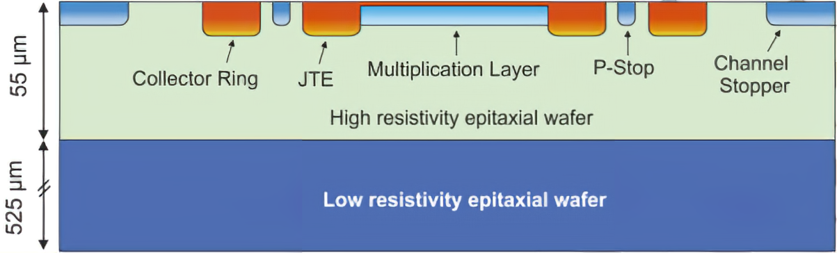
LGADs are semiconductor detectors designed for timing applications. They are constructed as avalanche diodes, with a highly-doped layer introduced to establish a region of very high electric field. This electric field is responsible for initiating the avalanche multiplication of primary electrons, generating additional electron-hole pairs. A schematic cross-section of a standard pad-like LGAD is illustrated in Figure 1. The LGAD structure is carefully engineered to achieve a moderate gain and operate effectively across a wide range of reverse bias voltages before reaching breakdown.
We present a radiation tolerance study performed on LGAD with a carbon-enriched multiplication layer. The LGAD sensors were manufactured at IMB-CNM (Institute of Microelectronics of Barcelona, Spain) [4], with the same processing as the one used in [6]222The sensor production mentioned in this reference has been developed without carbon enrichment. The LGADs are designed with a shallow gain layer doping profile which is characterized by a maximum of the doping concentration in the region close to the junction and a relative broad implant [5].
Its performance was compared against LGADs with identical layout and manufacturing processing, but without carbon enrichment. The LGADs were irradiated with neutrons at the TRIGA reactor in Ljubljana up to a fluence of . The degradation of its timing performance and charge collection with fluence is reported.
2 Samples Description
The IMB-CNM carried out a dedicated LGAD production for studying the effects of carbon on the broad multiplication layer that has been used up to now in its LGAD productions. The LGADs were manufactured on 6-inch diameter epitaxial wafers with active layer thickness and support wafer thickness. The Handle wafer has a resistivity of and the substrate resistivity is about . This Run was carried out on epitaxial wafers (Run#15246, 6LG3 process), and is the first run that implemented the carbon enrichment of the gain layer [7]. The run included matrices of different number of pads, 11 (single diodes), 22, 55, 1616 and 1632 where each pad is \qtyproduct1.3 x 1.3\squared.
Results shown in this work refer to wafers W8 and W10. The manufacturing parameters of these two wafers are described in table 1 including the gain layer depletion voltage measured before dicing the wafer, the boron dose and the Dry Oxidation Time (DOT). It is important to mention that the main difference between these two wafers is the implementation of carbon to the gain layer of wafer W8 in contrast with W10 that has a standard configuration consisting solely of boron implantation. Employing carbon co-implantation on the gain layer for the LGAD sensors manufacturing is effective in reducing the effects of the acceptor removal mechanism [8] which is an indicator of the degradation of the gain caused by radiation damage. In section 3.3 we show results on the acceptor removal effect on these carbonated sensors.
| Wafer | Carbonated | Standard |
|---|---|---|
| Gain layer depletion Voltage | 30 | 30 |
| Boron dose () | 1.9 | 1.9 |
| Carbon dose () | 10 | - |
| Dry oxidation time DOT (min) | 180 | 180 |
Measurements were conducted at Instituto de Física de Cantabria (IFCA) in order to characterize sensors from both wafers. Table 2 shows a summary of the sensors measured in the radioactive source setup. Two carbonated and three non-carbonated (standard) were kept as reference. For radioactive source measurements, samples are arranged in stacks of 3 sensors, where one non-irradiated sensor from W10 was used as a reference. Sensors were irradiated with neutrons to 3 different fluences: , and , in the TRIGA Mark II reactor333Capable of yield a maximum flux of around [12] in its central part. of the Jožef Stefan Institute (JSI) [9] at Ljubljana (Slovenia). The standard sensors at the highest fluence were not available for this study.
| Carbonated | Standard | Fluence () |
|---|---|---|
| 2 | 3 | 0 |
| 2 | 2 | |
| 2 | 2 | |
| 2 | - | 1.5 |
The total number of sensors measured in electrical characterization is higher than the ones measured in the radioactive source setup as we will see in section 3.
3 Electrical Characterization
The Current-Voltage (IV) and Capacitance-Voltage (CV) characteristics were measured in a probe station equipped with a thermal chuck. The measurements were performed before and after irradiation. Measurements of non-irradiated devices were conducted at room temperature, while the irradiated devices were measured at a temperature of . The ohmic contact side (backside) of the sensors was connected to ground, while the cathode and the guard-ring were connected to High-Voltage (HV). For the IV measurement, the guard-ring and main diode currents were determined independently using two different Keithley 2410 sourcemeters [10] that allows supply the High-Voltage for the diode and measure the currrent at the same time. For the CV measurement, the guard-ring and the main diode were connected to HV using Keithley 2410 sourcemeters and read by a Quadtech 1920 LCR-meter [11] connected through a decoupling box. The circuit model used to determine the capacitance was a parallel RC circuit and the measurements were carried out at () frequency before (after) irradiation. In total, 44 LGADs were measured in IV and approximately half of them in CV before irradiation.
3.1 Current-Voltage characteristic
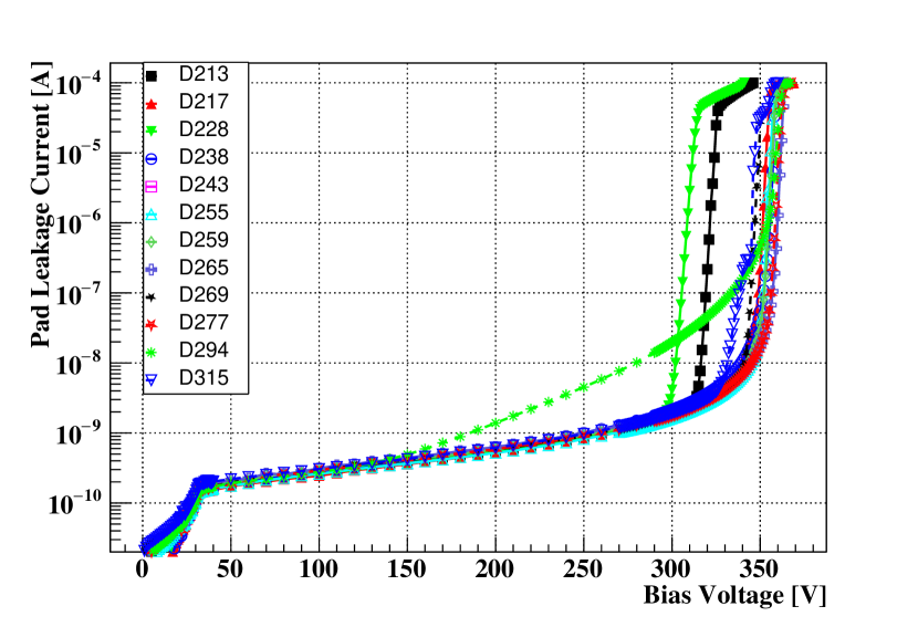
Figure 2 displays the main diode current versus reverse bias for both types of sensors before irradiation and at room temperature. Across most of the bias voltage range, the current for both types of sensors is below the nanoampere. The breakdown voltage was determined for both carbonated and standard sensors estimating the change in the slope by using the method described in section 3.3, and found to be in the range of to and to for carbonated and standard samples respectively. In general, the for both wafers has low dispersion, with an RMS value of approximately () for carbonated (standard) LGADs. The leakage current of carbonated sensors in the gain layer (GL) region (about ) is higher (around ) than the standard sensors (around ) as expected [14] since the carbon enhancement increases the defects in the gain-layer.

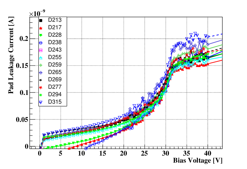
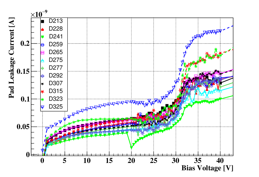
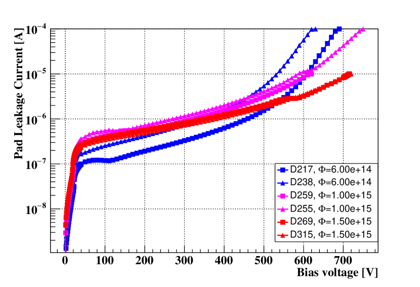
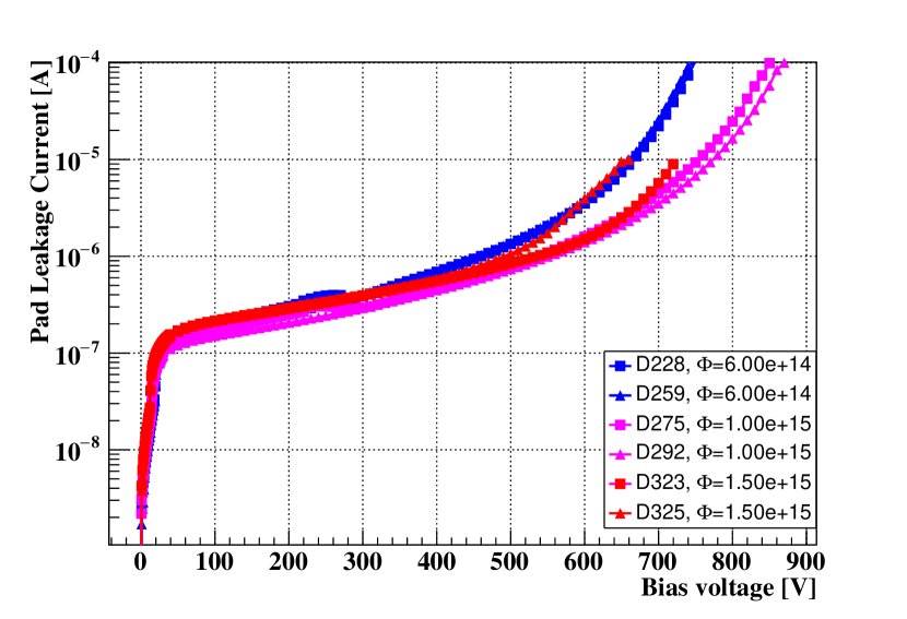
A second electrical characterization at was made after irradiation of the devices, from which two sensors of every type and fluence ( and ) are presented in Figure 3. In plot (a) the pad leakage current of the carbonated sensors can be observed as a function of the reverse bias. The shift to higher values for the regimes with increasing irradiation is clearly visible, starting from about for the lowest fluence and between to for the more irradiated, in contrast to the initial - range for the non-irradiated devices. The maximum applied voltage was not increased further to avoid fatal Single Even Burnouts (SEBs) [13]. In the case of the standard sensors on plot (b), their starts from for lowest fluence and about for the rest of fluences. In both cases, the increase of the indicates the degradation of the gain layer due to irradiation fluence. The displacement which is another important indicator of this degradation caused by the irradiation will be presented in section 3.3.
3.2 Capacitance-Voltage characteristic
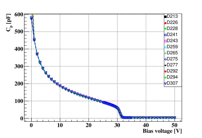
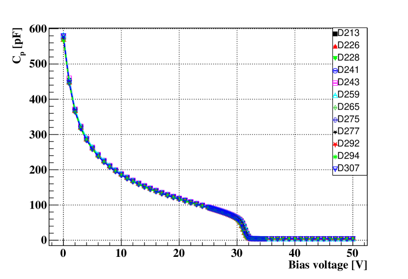
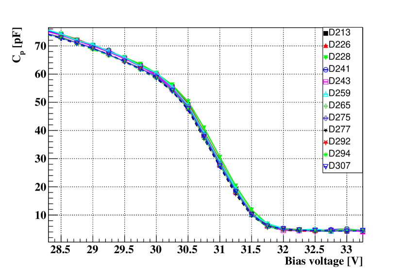
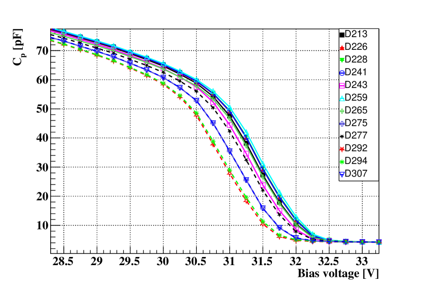
The capacitance of the bare sensors was measured before irradiation at room temperature with the guard-ring connected and at a frequency of on the LCR-meter. Plots (a) and (b) in Figure 4 show the curves of the capacitance versus the reverse bias applied for the carbonated and standard samples, respectively. High homogeneity and reproducibility are evident in these curves. The CV curves start with a smooth decrease in capacitance in the gain layer region that ends at approximately for both carbonated and standard samples, representing the depletion voltage . This is followed by another kink in the curve, indicating the depletion of the bulk, which ends with a final capacitance () of about for both types of wafers, at voltages above (carbonated) and (standard). This is consistent with the fact that all sensors have the same dimensions. Plots (c) and (d) show an enlarged view of the capacitance curves in the gain layer region, where it can be observed that, in general, the curves of all samples, carbonated and standard, follow a similar shape, but the of the samples is less dispersed in the presence of carbon.
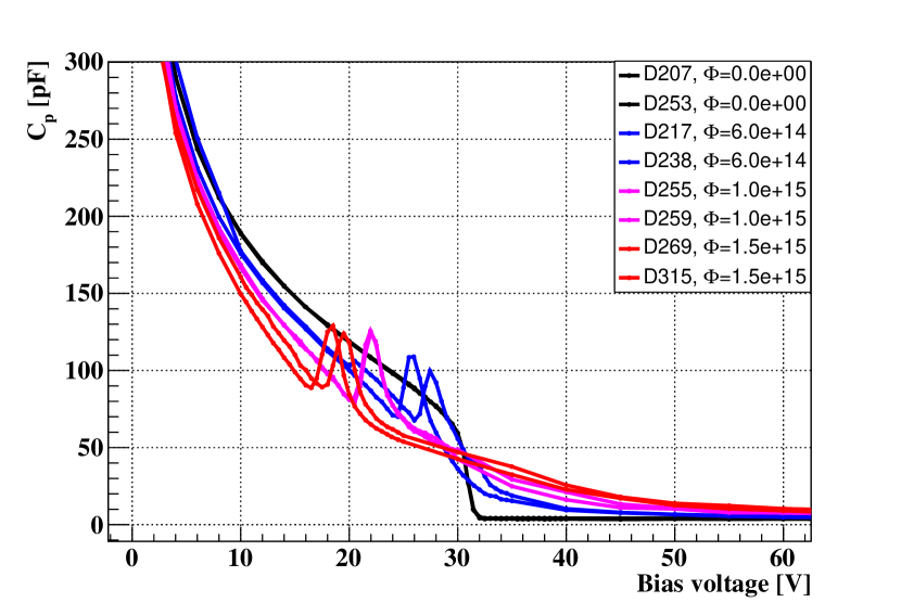
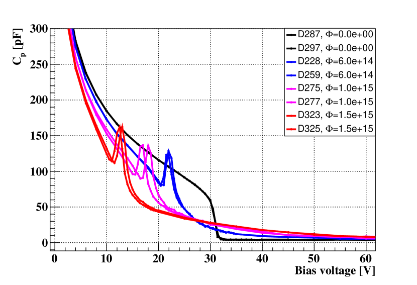
The pad capacitance after irradiation of the samples is depicted as a function of the applied bias in Figure 5. To better observe the region [15], these measurements were conducted at a temperature of with a low frequency of configured in the LCR-meter. The remaining LCR-meter settings remained consistent with those used before irradiation.
For the irradiated devices we can see an increase of the capacitance until a local maximum that has been concluded to be related with the presence of the multiplication layer [16]. In plot (a), the carbonated samples exhibit a noticeable degradation in the gain layer due to irradiation, resulting in a corresponding shift of proportional to the fluence (lower at higher fluences). Plot (b) displays the curves of the standard samples, where a reduction in is also evident as a consequence of irradiation. However, the values are lower compared to the carbonated samples. For instance, at the highest fluence, the for the carbonated sensor is approximately while for the standard sensor, it is around . From these CV characteristics, we have considered the as the last point before the increase of the capacitance, since this coincides with the extracted from IV characteristics.
3.3 Determination of Acceptor Removal Coefficient
It has been shown that LGAD sensors experience a reduction in gain after irradiation with charged hadrons or neutrons [18]. This reduction can be attributed to the initial acceptor removal mechanism, involving the gradual deactivation of acceptors forming the GL [19], specifically boron (B) in this case.
As irradiation deactivates the boron implanted in the GL of LGAD sensors, the reverse bias required to fully deplete this gain layer, denoted as , decreases compared to the pre-irradiation state. This reduction in provides an indication of the remaining active boron in the GL. Assuming uniform boron removal throughout the multiplication layer and at a consistent rate, we can express as proportional to the boron concentration using the following equation:
| (1) |
Here, is the acceptor removal coefficient, and represents the gain layer depletion voltage corresponding to the given fluence . The coefficient is an indicator of the degradation suffered by the multiplication layer and thus the lower value, the more radiation hard the sensor is.
After irradiation, a second electrical characterization was conducted to analyze the degradation of the gain layer, starting with the extraction of and determining the Acceptor Removal Coefficient. A crucial aspect of this study is examining the effect of carbon enrichment in the GL compared to the standard boron implantation and how it influences the acceptor removal coefficient for both types of sensors.
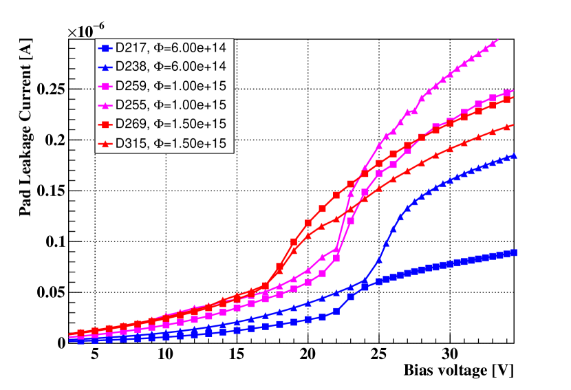
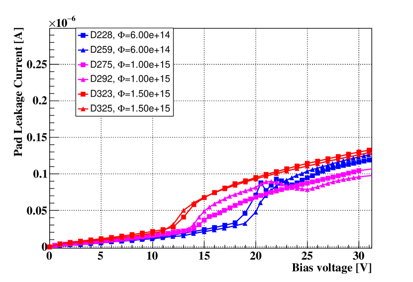
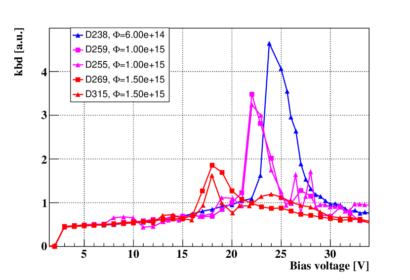
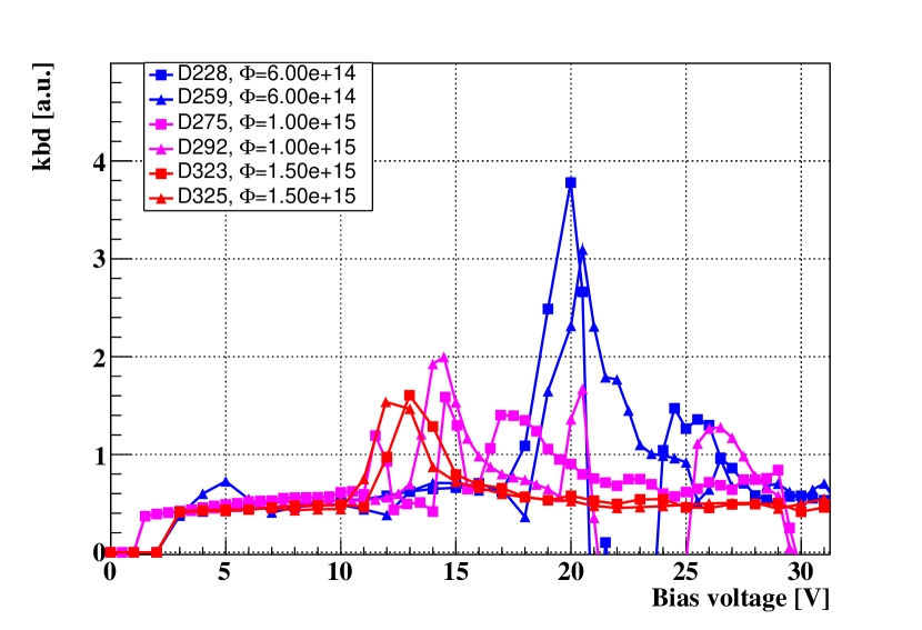
Figure 6 contains plots of IV curves, centered around the GL region, of the carbonated (a) and standard (b) sensors. In the bottom (plots (c) and (d)) we show a variable constructed as the derivative of the current weighted by the ratio of current over voltage:
| (2) |
This variable was first introduced in [20] as an automatic estimator of the breakdown voltage and is used here to identify the change in slope indicating the transition from the GL to the bulk [21]444Other methods to calculate the , see: [22]. The values extracted from the electrical characterization are shown in table 3. From these values the degradation of the GL can be calculated fitting the dependence of with fluence, according to Equation 1.
| from IV (V) | from CV (V) | |||
|---|---|---|---|---|
| Fluence () | Carbonated | Standard | Carbonated | Standard |
| 0 | ||||
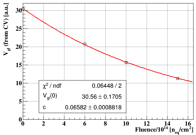
The resulting curve for versus fluence, along with its fit, is presented in Figure 7 for both carbonated and standard devices. The resulting coefficients are and , respectively. This outcome indicates that the addition of carbon in the co-implantation of the gain layer results in a smaller degradation of boron and, consequently, an improvement in the resistance to radiation in these LGADs. These results are also consistent with the evidence of better performance of carbonated sensors seen in the improvement in acceptor removal from other LGAD manufacturers. [17]

4 Radioactive Source Characterization
The radioactive source setup at IFCA consists of a metallic box enclosing a stack of three sensors. Each sensor is mounted on a simple passive PCB that provides electrical connections. The box is placed inside a climate chamber that allows for temperature cycles. An encapsulated Sr90 radioactive source with an activity of is positioned on top of the stack, ensuring no physical contact with the samples. The alignment of sensors in the stack is maintained by gluing the devices using a mechanical template. To measure the current induced, an external low-noise current amplifier (with a nominal gain of ) [23] is used for amplification. The readout is performed using an oscilloscope with a sampling rate of . The readout is triggered by a triple coincidence. The samples measured in the radioactive source setup are detailed in Table 2. The third detector in the stack was always a non-irradiated LGAD device, serving as a reference.
4.1 Charge Collection
The collected charge per particle is calculated as the integral of the voltage pulse (Figure 8 (a)). The total distribution of charge for a single detector, shown in Figure 8 (b), is fitted by the convolution of a Landau with a gaussian. The most probable value of this distribution is used as an estimation of the total collected charge.
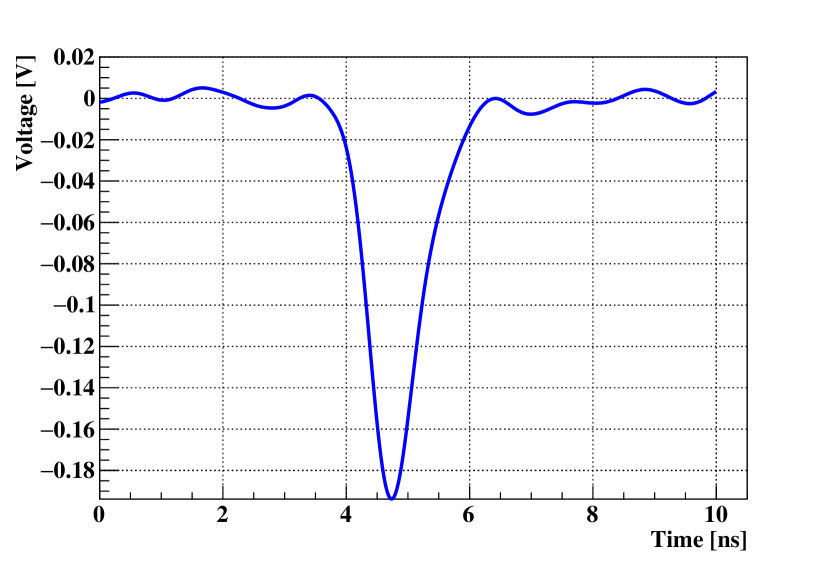
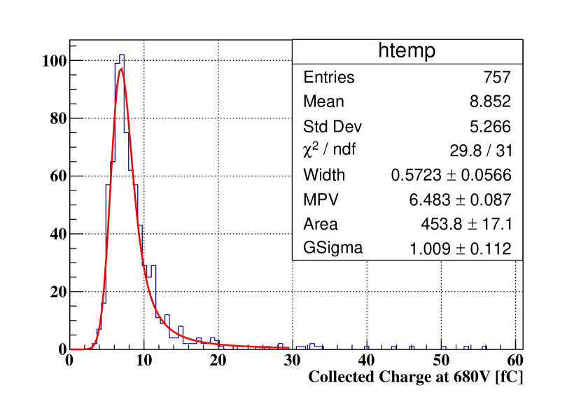
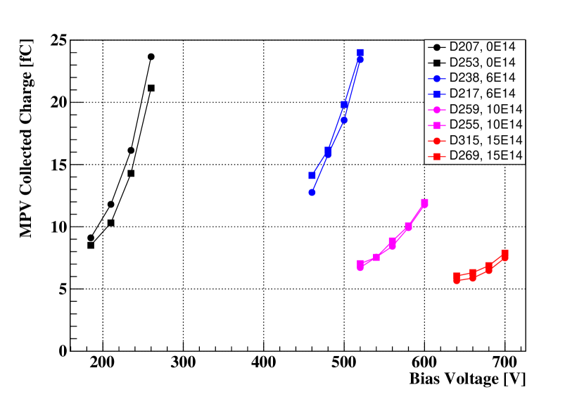
Figure 9 shows the charge collected as a function of the bias voltage for different fluence. There is a clear separation between the samples in terms of the reverse bias regions. To achieve the same charge, the higher irradiated samples require higher bias. There is good repeatibility of the collected charge for samples irradiated to the same fluence. The carbonated sensors can be operated at a bias lower than the standard ones. As an example, are needed to collect in a carbonated sample irradiated to a fluence of while are needed for the standard ones. Since this difference is not too evident comparing the non-irradiated sensors of both GL configurations, it is an indication that the carbon leads to a radiation resistance on these LGADs.
4.2 Time Resolution
The time resolution of a sensor can be calculated as the standard deviation of the distribution of the differences in arrival time (ToA) of the sensor with respect to a well-known reference. If a reference is not available, then three detectors can be measured simultaneously [24], and the individual time resolutions calculated from the three relative differences (1-2, 1-3, 2-3).
The time of arrival (ToA) is computed as the time when a pulse crosses a threshold. Since pulses of different amplitudes arriving at the same time will cross a threshold at different times (time walk effect), the pulses are corrected using a Constant Fraction Discrimination (CFD) algorithm.
The fitted widths: , , and of the difference distributions are used to determine the time resolution of the three sensors (, , ) by solving the system of equations:
| (3) |
with errors (, and ) given by:
| (4) |
where is the error in the value .
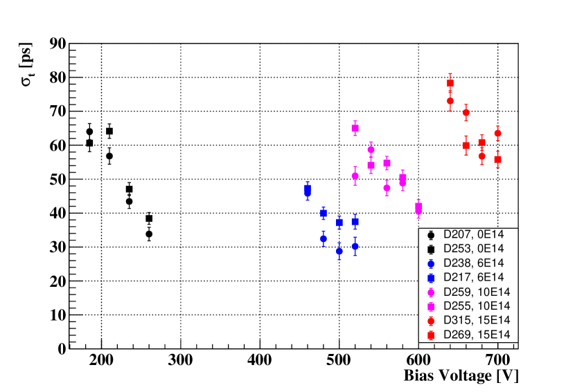
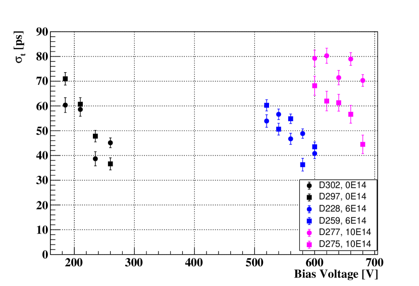
This method was applied to all samples of this study, maintaining the non-irradiated sensor mentioned in sec. 4 as reference. The resulting time resolution of carbonated (plot (a)) and standard (plot (b)) sensors is presented in Figure 10. As the fluence increases, the voltage needed to achieve the same time resolution also increases. Time resolution improves as bias voltage grows. Finally, the bias voltage needed to reach values belos time resolution is smaller in carbonated detectors.
5 Noise Study
To ensure the functionality of the sensors, a noise study was carried out on the carbonated samples. Although this noise affects both carbonated and non-carbonated samples, this study was not carried out on the standard sensors. Key parameters considered include the baseline noise level and the presence and frequency of micro-discharges (thermally generated spurious pulses).
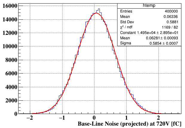
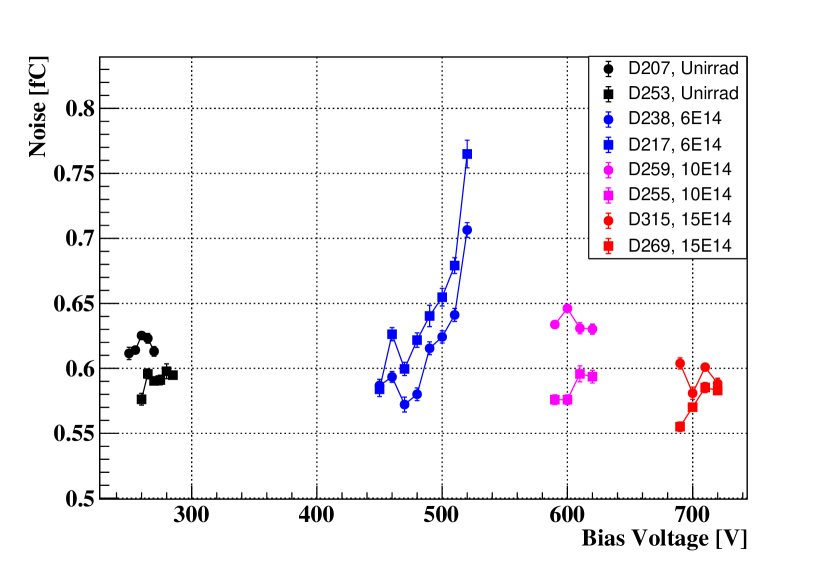
The noise of the carbonated samples was investigated using a random trigger. Two hundred events (waveforms) per bias voltage were collected in a histogram (depicted in Figure 11 (a)), and the Gaussian width of the resulting distribution was taken as the noise value. The increase in noise with voltage was examined for various fluence values and summarized in Figure 11 (b). The noise increase is more pronounced for the samples, but does not prevent operation. The measurements were performed at .
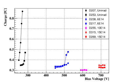
The amplitude of spurious, dark counts (thermally generated), was also measured at (and beyond) the operation voltage for each fluence with a trigger of threshold level of , this threshold corresponds to approximatly 6 MIPs for a PIN diode (without gain) of of active thickness. Again, no radioactive source was employed for this study. The spurious pulses appeared in all the carbonated samples near the breakdown voltage. Figure 12 shows the charge content of these pulses. The charge of the spurious pulses was calculated by means of the amplitude to charge correlation from the measurements taken in section 4. For the non-irradiated and lowest fluence samples, a scaling trend with the bias voltage can be seen, while for the two higher fluence samples no increase was observed near breakdown.
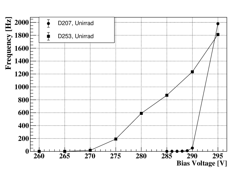
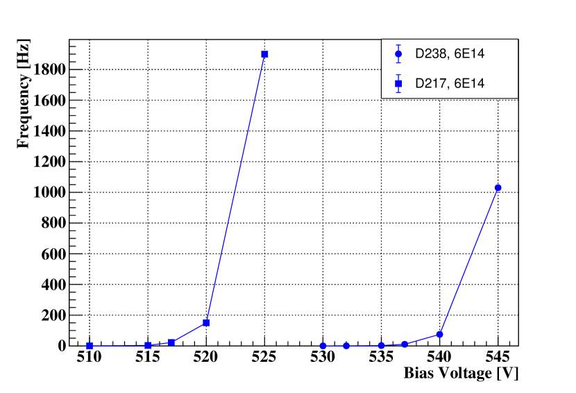
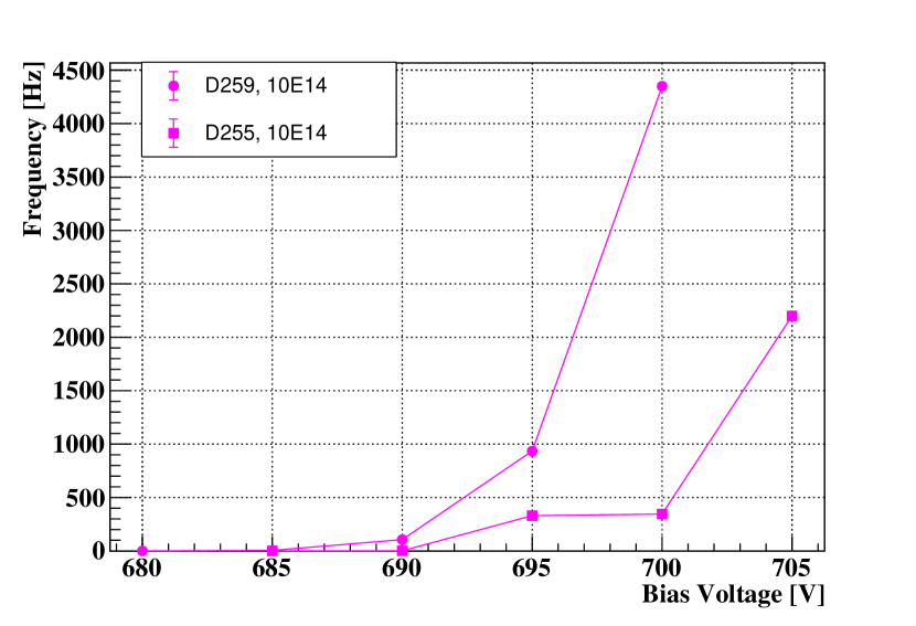
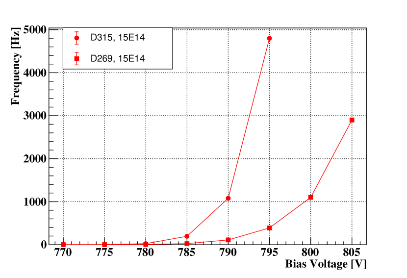
Since the pulse rate may be limited by the digital Scope Band-Width, we decided to use NIM [25] electronic modules, specifically a Discriminator, a Timer and a Counter to obtain the pulse rate of the Dark Counts. The minimum threshold of the discriminator was that is higher than the used with the oscilloscope, resulting in a underestimation of the spurious pulse rate. The resulting rates for the different samples are shown in Figure 13. The plot starts at the operating voltage for each detector, that is the bias voltage needed to obtain (CMS constraint): and respectively for the fresh, , and irradiated samples. The presence of spurious pulse was attributed to the short distance between the end of the gain layer and the p-stop at the periphery of the pad (see Figure 1). For this production this distance was 23.5 , which was decided in order to minimize, as much as possible, the inter-pad distance in the multi-pad matrix-type LGADs.
6 Conclusions
In this study, the first manufacturing run at IMB-CNM of Low Gain Avalanche Detectors with a carbon-enriched multiplication layer was investigated for its radiation tolerance compared to conventional LGADs. The sensors were subjected to neutron irradiation at the TRIGA reactor in Ljubljana, reaching a fluence of . The results, reported in terms of degradation in timing performance and charge collection with increasing fluence, demonstrated the potential benefits of carbon enrichment in mitigating radiation damage effects, particularly the acceptor removal mechanism. The acceptor removal constant of carbonated samples with respect to the standard samples was reduced by more than a factor of two.
Time resolution and the collected charge was studied on the Radioactive Source (RS) setup for samples non-irradiated and irradiated up to fluences of . As expected, degradation of the time resolution and the collected charge due to the irradiation was evidenced. The time resolution of the carbonated samples, at a fluence of at the maximum bias voltage of achieved before the breakdown regime, is of while at same fluence and bias voltage for the Standard LGADs is about , and at a maximum bias voltage of is around . Confirming the better radiation tolerance of the carbonated samples as it was the case of the acceptor removal coefficient.
Additionally, a noise analysis was conducted on the samples. The investigation focused on key parameters, including baseline noise level and the occurrence and frequency of micro-discharges, which may manifest as spurious pulses in silicon detectors due to thermal generation. The noise of carbonated samples was analyzed using a random trigger, measuring signal width without a radioactive source. The resulting noise values were examined across various fluences, as depicted in Figure 12. Despite a more pronounced increase in noise for samples irradiated to , the elevated noise levels did not impede the device’s operation. Additionally, spurious, thermally generated pulses were measured beyond the operational voltages, showing a scaling trend with bias voltage for non-irradiated and lower fluence samples, while higher fluence samples exhibited no increase near breakdown.
Acknowledgments
This work was developed in the framework of the CERN RD50/DRD3 collaboration and has been funded by the Spanish Ministry of Science and Innovation (MCIN/AEI/10.13039/501100011033/) and by the European Union’s ERDF program “A way of making Europe”. Grant references: PID2020-113705RB-C31, PID2020-113705RB-C32 and PID2021-124660OB-C22. Also, it was supported by the following European funding programs: the European Union’s Horizon 2020 Research and Innovation (under Grant Agreement No. 101004761, AIDAInnova) and NextGenerationEU (PRTR-C17.I1). This work was also been developed in the framework of the ”Ayudas Maria Zambrano para la atraccion de talento internacional”, co-funded by the Ministry Of University of Spain and the European Union NextGenerationEU, reference code: C21.I4.P1; under the framework of ”Ayudas para contratos predoctorales para la formación de doctores 2019”, co-funded by the European Social Fund program ”El FSE invierte en tu futuro” with grant reference: PRE2019-087514; and the Plan Complementario en el Área de Astrofísica y Física de Altas Energías, financed by Next Generation EU funds, including the Recovery and Resilience Mechanism (MRR), the Recovery, Transformation and Resilience Plan (PRTR) and the Autonomous Community of Cantabria.
References
- [1] CERN, High-Luminosity Large Hadron Collider (HL-LHC): Technical design report, CERN Yellow Reports: Monographs, 2020, doi:10.23731/CYRM-2020-0010, https://cds.cern.ch/record/2749422.
- [2] CMS Collaboration, Technical proposal for a MIP timing detector in the CMS experiment phase 2 upgrade, CERN Technical Report, CERN-LHCC-2017-027, LHCC-P-009, Dec. 2017, https://cds.cern.ch/record/2296612.
- [3] ATLAS Collaboration, Technical Proposal: A High-Granularity Timing Detector for the ATLAS Phase-II Upgrade (CERN-LHCC-2018-023. LHCC-P-012). Geneva: CERN, https://cds.cern.ch/record/2623663.
- [4] Institute of Microelectronics of Barcelona (IMB-CNM), 2023, https://www.imb-cnm.csic.es/en.
- [5] I. Cortés, P. Fernández-Martínez, D. Flores, S. Hidalgo, J. Rebollo, Gain estimation of RT-APD devices by means of TCAD numerical simulations, Proceedings of the 8th Spanish Conference on Electron Devices, CDE-2011, https://doi.org/10.1109/SCED.2011.5744152.
- [6] E. Currás, A. Doblas, M. Fernández, D. Flores, J. González, S. Hidalgo, R. Jaramillo, M. Moll, E. Navarrete, G. Pellegrini, I. Vila, Timing performance and gain degradation after irradiation with protons and neutrons of Low Gain Avalanche Diodes based on a shallow and broad multiplication layer in a float-zone 35 µm and 50 µm thick silicon substrate, Nuclear Instruments and Methods in Physics Research, A: Accelerators, Spectrometers, Detectors and Associated Equipment, 2023, 51–55, https://doi.org/10.1016/j.nima.2023.168522.
- [7] J. Villegas, S. Hidalgo, A. Merlos, N. Moffat, G. Pellegrini, M. Fernández, R. Jaramillo, E. Navarrete, A. K. Sikdar, I. Vila, Measurements on last IMB-CNM LGADs production, The 40th RD50 Workshop, 2022, https://indico.cern.ch/event/1157463/contributions/4922755/.
- [8] M. Ferrero, R. Arcidiacono, M. Barozzi, M. Boscardin, N. Cartiglia, G. Betta, F. Dalla, Z. Galloway, M. Mandurrino, S. Mazza, G. Paternoster, F. Ficorella, L. Pancheri, W. Sadrozinski, F. Siviero, V. Sola, A. Staiano, A. Seiden, M. Tornago, Y. Zhao, Radiation resistant LGAD design, Nuclear Instruments and Methods in Physics Research Section A: Accelerators, Spectrometers, Detectors and Associated Equipment, 0168-9002, doi: 10.1016/j.nima.2018.11.121, 2019, https://www.sciencedirect.com/science/article/pii/S0168900218317741.
- [9] D. Žontar, V. Cindro, G. Kramberger, M. Mikuž, Time development and flux dependence of neutron-irradiation induced defects in silicon pad detectors, Nuclear Instruments and Methods in Physics Research, A 426, 1999, 51–55, doi: 10.1016/S0168-9002(98)01468-5, https://www.sciencedirect.com/science/article/pii/S0168900298014685.
- [10] Tektronix, Keithley 2400 Standard Series SMU, 2023, https://www.tek.com/en/products/keithley/source-measure-units/2400-standard-series-sourcemeter.
- [11] IET Labs Inc, IET/QuadTech 1910/1920 1 MHz LCR Meter, 2023, https://www.ietlabs.com/1900-lcr-meter.html.
- [12] European Nuclear Experimental Educational Platform (ENEEP), IJS Ljubljana, 2019-2022, https://www.eneep.org/about/ijs/.
- [13] Lipton, J. Ronald, LGAD Single Event Burnout Studies, United States, 2021, https://doi.org/10.2172/1841397.
- [14] E-L. Gkougkousis, L. Castillo Garcia, S. Grinstein, V. Coco, Comprehensive technology study of radiation hard LGADs, J. Phys.: Conf. Ser. 2374 012175, 2022, doi: 10.1088/1742-6596/2374/1/012175, https://iopscience.iop.org/article/10.1088/1742-6596/2374/1/012175.
- [15] D. Campbell, A. Chilingarov, T. Sloan, Frequency and temperature dependence of the depletion voltage from cv measurements for irradiated si detectors, Nuclear Instruments and Methods in Physics Research Section A: Accelerators, Spectrometers, Detectors and Associated Equipment 492, (3), 2002, 402–410, https://www.sciencedirect.com/science/article/pii/S0168900202013530.
- [16] M. Wiehe, M. Fernández, S. Hidalgo, M. Moll, S. Otero, U. Parzefall, G. Pellegrini, A. Barroso, I. Vila, Study of the radiation-induced damage mechanism in proton irradiated low gain avalanche detectors and its thermal annealing dependence, Nuclear Instruments and Methods in Physics Research Section A: Accelerators, Spectrometers, Detectors and Associated Equipment 986, 2021, https://www.sciencedirect.com/science/article/pii/S0168900220312110.
- [17] K. Wu, X. Jia, T. Yang, M. Li, W. Wang, M. Zhao, Z. Liang, J. Guimaraes, Y. Fan, H. Cui, A. Howard, G. Kramberger, X. Shi, Y. Heng, Y. Tan, B. Liu, Y. Feng, S. Li, M. Li, C. Yu, X. Yang, M. Zhai, G. Xu, G. Yan, Q. Zhai, M. Ding, J. Luo, H. Yin, J. Li, Design and testing of LGAD sensor with shallow carbon implantation, Nuclear Instruments and Methods in Physics Research Section A: Accelerators, Spectrometers, Detectors and Associated Equipment, 2023, doi: 10.1016/j.nima.2022.167697, https://www.sciencedirect.com/science/article/pii/S0168900222009895.
- [18] Z. Galloway, V. Fadeyev, P. Freeman, E. Gkougkousis, C. Gee, B. Gruey, C. Labitan, Z. Luce, F. McKinney-Martinez, H. F. Sadrozinski, A. Seiden, E. Spencer, M. Wilder, N. Woods, A. Zatserklyaniy, Y. Zhao, N. Cartiglia, M. Ferrero, M.Mandurrino, A. Staiano, V. Sola, R. Arcidiacono, V. Cindro, G. Kramberger, I. Mandić, M. Mikuž, M. Zavrtanik, Properties of HPK UFSD after neutron irradiation up to 6e15 n/cm2, Nuclear Instruments and Methods in Physics Research, A: Accelerators, Spectrometers, Detectors and Associated Equipment, 2019, doi: 10.1016/j.nima.2019.05.017, https://www.sciencedirect.com/science/article/pii/S0168900219306278.
- [19] G. Kramberger, M. Carulla, E.Cavallaro, V. Cindro, D. Flores, Z. Galloway, S. Grinstein, S. Hidalgo, V. Fadeyev, J. Lange, I. Mandić, G. Medin, A. Merlos, F. McKinney-Martinez, M. Mikuž, D. Quirion, G. Pellegrini, M. Petek, H. Sadrozinski, A. Seiden, M. Zavrtanik, Radiation hardness of thin Low Gain Avalanche Detectors, Nuclear Instruments and Methods in Physics Research, A: Accelerators, Spectrometers, Detectors and Associated Equipment, 2018, doi: 10.1016/j.nima.2018.02.018, https://www.sciencedirect.com/science/article/pii/S0168900218301682.
- [20] N. Bacchetta, D. Bisello, A. Candelori, M. Da Rold, M. Descovich, A. Kaminski, A. Messineo, F. Rizzo, G. Verzellesi, Improvement in breakdown characteristics with multiguard structures in microstrip silicon detectors for CMS, 2001, doi: 10.1016/S0168-9002(00)01207-9, https://www.sciencedirect.com/science/article/pii/S0168900200012079.
- [21] M. Fernandez, Status report on the radiation tolerance assessment of CNM AIDA2020v2 and HPK-P2 LGADs., 16th Trento Workshop on Advanced Silicon Radiation Detectors, 2021, https://indico.cern.ch/event/983068/contributions/4223223/.
- [22] V. Gkougkousis, Radiation hardness of 6” SoI CNM LGADs, 35th RD50 workshop, 2019, https://indico.cern.ch/event/855994/contributions/3636943/.
- [23] CIVIDEC Instrumentation, TCT Amplifier for Detector Physics, integrated Bias-Tee, https://cividec.at/electronics-C2-TCT.html.
- [24] P. McKarris, M. C. Vignali, M. O. Wiehe, Commissioning of a beta setup for time resolution measurements, DT 2019 Summer students, 2019, https://indico.cern.ch/event/840877/.
- [25] Costrell, et al., Standard NIM Instrumentation System 1990, doi: 10.2172/7120327, https://www.osti.gov/biblio/7120327.