Ultrafast optical switching to a heterochiral charge-density wave state
Optical control of correlated electronic states promises unprecedented tunability of novel functional materials Bao2022 ; Torre2021 ; Basov2017 . Tailored optical excitations can steer a system along non-equilibrium pathways to metastable states with specific structural or electronic properties Stojchevska2014 ; Horstmann2020 ; Rini2007 . A much-desired feature is the reproducible and ultrafast switching to functional states. The light-induced hidden state of 1T-TaS2, with its strongly enhanced conductivity and exceptionally long lifetime, represents a unique model system for studying the switching of correlated electronic states using femtosecond optical stimuli Stojchevska2014 ; Maklar2023 . However, despite intense investigation, the switching mechanism and the structural origins of the distinctive electronic properties of the hidden state have not been fully uncovered. Here, we use surface-sensitive electron diffraction in combination with a femtosecond optical quench to reveal coexistent charge-density wave chiralities as a new structural feature of the hidden state. We find that a single-pulse optical quench produces a state with long-range structural order and different weights of the two chiral enantiomorphs of the charge-density wave. Harnessing a double-pulse optical quench Horstmann2020 ; Maklar2023 ; Hase2015 ; Weiner1990 , we trace the origin of the mixed chirality to the transient electronic excitation of the host crystal. The coexistent long-range-order of both chiralities suggests the presence of extended heterochiral charge-density wave interfaces, which results in a higher-level, fractal-type moiré superstructure. Density functional theory simulations for such a charge-density wave moiré superstructure reveal multiple flat bands, Dirac cones, and a kagome electronic subsystem around the Fermi energy. Our findings shed light on novel electronic properties gained by chiral interface engineering, and create avenues for light-induced moiré superstructures in quasi-two-dimensional materials.
Ultrafast control of functional materials via non-equilibrium pathways promises access to tailored electronic and structural properties Bao2022 ; Torre2021 ; Basov2017 . A particularly prominent example is the 1T-TaS2 hidden state Stojchevska2014 , which may enable novel non-volatile all-electronic memory devices Vaskivskyi2016 . The long-lived metastable hidden state exhibits metallic conductivity Stojchevska2014 ; Gao2022 ; Svetin2017 and is generated from the insulating low-temperature commensurate charge-density wave phase (C-phase) vonWitte2019 by applying single laser or voltage pulses Stojchevska2014 ; Gerasimenko2019 ; Cho2016 ; Ma2016 ; Vaskivskyi2015 . Structural changes associated with this state have been probed by scanning tunneling microscopy (STM) and X-ray diffraction, yielding an emergent mosaic network of domain walls and the breakdown of interlayer dimerization Gerasimenko2019 ; Cho2016 ; Ma2016 ; Stahl2020 . However, a unifying picture that explains the structural origin of metallic conductivity and long-term stability, as well as the possible role of quench-induced disorder, remains to be developed.
In the present work, we reveal a new structural characteristic concurring with the hidden state: coexistent charge-density wave (CDW) chiralities. Using low-energy electron diffraction (LEED) Vogelgesang2018 following a single-pulse optical quench Stojchevska2014 ; Vaskivskyi2015 ; Gao2022 ; Gerasimenko2019 ; Stahl2020 , our experiments demonstrate the emergence of a long-range-ordered CDW chirality opposite to that of the initial state. The electronic origin of this structural transformation is verified by double-pulse excitation Maklar2023 ; Ravnik2018 . Fluence-dependent diffraction intensities of the newly formed chirality show a threshold behavior for 13 measured samples. The identified threshold fluence varies by about a factor of 3 among the ensemble of crystals, with an average value of 1.2 mJ/cm, in accordance with previously observed thresholds for hidden-state generation Stojchevska2014 ; Gerasimenko2019 ; Stahl2020 . At high fluence, most specimens exhibit a saturated diffraction intensity of the minority chirality between 2 % and 7 % of that of the majority chirality, while two samples reach about 10 % without a clear sign of saturation. Our study implies extended CDW moiré interfaces present in the laser-induced state, for which DFT simulations predict a new type of kagome charge order that supports in-plane metallic conductivity. Alongside disordered CDW stacking arrangements Cho2016 ; Ma2016 , such heterochiral interfaces may contribute to the electronic properties of the hidden state, and more generally, suggest active laser control of interface chirality also in other contexts Ohta2021 ; Stojchevska2018 ; Song2022 ; Liu2023 .
Results
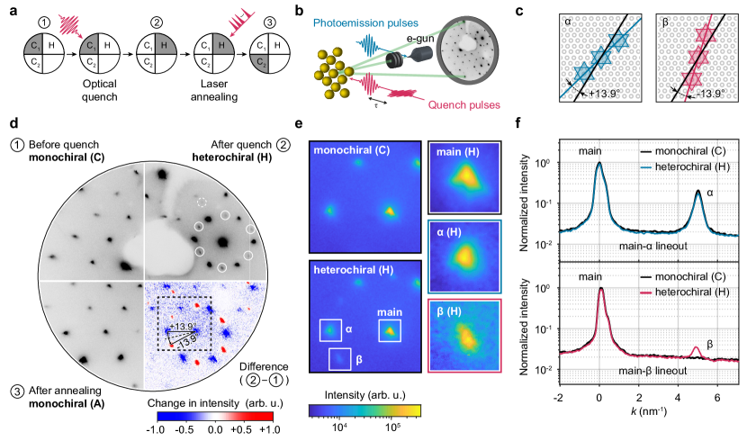
We probe the structural changes of optically quenched 1T-TaS2 crystals with high-coherence microbeam LEED Vogelgesang2018 . Our most important observation is the emergence of CDW diffraction peaks with a chirality opposite to that of the initial state (Fig. 1d, sample #1). Specifically, we find new CDW superstructure peaks at the opposite rotation angle with respect to the main lattice after the sample is quenched by a single laser pulse. In the absence of further perturbations, this new structural feature persists beyond several hours. We denote the CDW superstructure peaks in the initial C-phase as and the emergent peaks as . The intensity difference of images before and after the optical quench (bottom-right panel of Fig. 1d) highlights the suppression of the peaks and the emergence of the peaks in the heterochiral CDW state. A reversal to the initial LEED pattern, i.e., an erasing of the emergent peaks, can be achieved by illuminating the sample with a femtosecond laser pulse train for a duration of 1 s at a fluence of 0.5 mJ cm and a repetition rate of 100 kHz. Besides an occasional intensity decrease of the main lattice and peaks that was observed in some samples, the resulting monochiral state has a diffraction pattern (bottom-left panel of Fig. 1d) practically indistinguishable from that of the initial C-phase.
Close-ups of the diffraction patterns before and after the quench are displayed in Fig. 1e. It is evident that the spot profiles of the main lattice and peaks remain nearly unchanged after the optical quench, while the spot size of the new peaks is comparable to that of the peaks, as shown by the lineouts in Fig. 1f. Specifically, the minimum correlation lengths of the and chirality are determined as 22 nm and 24 nm, respectively (cf. Sec. I of Supplementary Information). Beyond the emergence of the chirality, we find no pronounced changes in the diffraction pattern besides a small intensity drop of the main lattice and peaks. Notably, there is no evidence of substantial linewidth broadening for the main lattice or peaks, which would indicate a significant increase of structural disorder. Together, this implies that the emergent chirality exhibits long-range structural order.
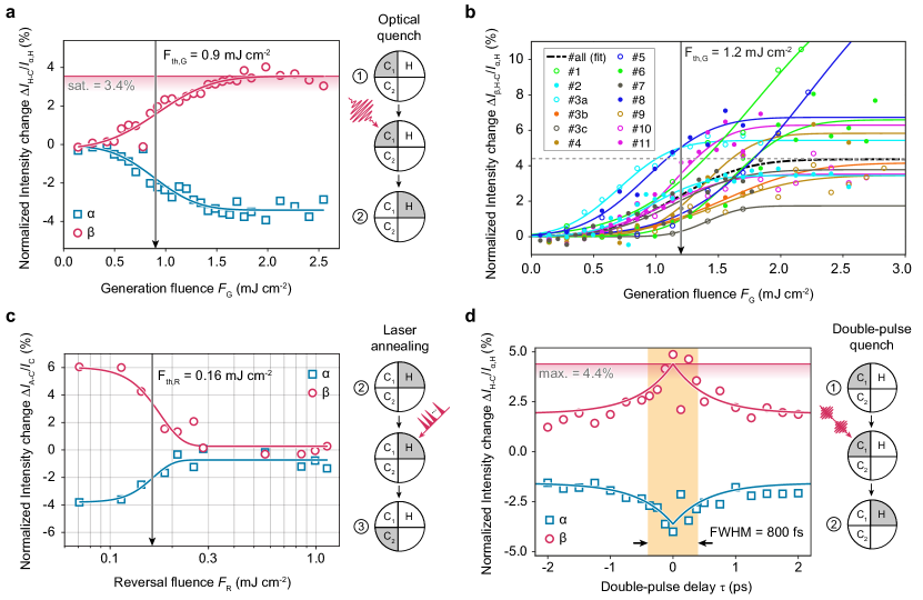
Figure 2a shows the emergence of peaks and a concurrent suppression of the peak intensity as a function of the single-pulse quench fluence. This measurement is carried out for one of the investigated samples with a randomized sequence (sample #2), demonstrating that the observations are not affected by sample deterioration. The intensity changes are normalized to the peak intensity in the heterochiral state, accounting also for the background. Overall, the intensity changes are on the order of few percent of the peak intensity. We find a threshold behaviour of the arising peak intensity at a fluence of mJ cm, which is in close correspondence to the threshold reported for preparing the hidden state Stojchevska2014 ; Gerasimenko2019 ; Stahl2020 . Above the fluence threshold, we observe a saturation in the peak intensity for this sample. Neither additional features in the diffraction pattern nor permanent sample damage are observed for the quench pulse fluence in the saturation regime (no sample damage was observed in LEED images for quench pulse fluences up to 3.4 mJ cm). Fluence-dependence measurements of 12 other samples (with a measurement sequence from low to high fluences) show a very similar behavior, albeit with somewhat varying threshold and saturation characteristics (Fig. 2b). We note that a comparable number of investigated samples did not show the formation of the heterochiral state, and some only did for a limited time after cleaving. Overall, a very high surface quality, low contamination, and likely low defect density appear to be a prerequisite for generating this state.
By repeatedly preparing the sample in the heterochiral state using a single-pulse quench at 1 mJ cm, we find a threshold for the reversal to the monochiral state at a fluence of mJ cm (Fig. 2c, sample #3a). In annealing the sample, a 100 kHz laser pulse train is applied for 1 s. Both the long lifetime and the comparatively low annealing threshold are clear evidence of metastability, as previously reported for the hidden state Stojchevska2014 ; Vaskivskyi2015 . The state’s high sensitivity to the surface quality also suggests that it resides in a particularly shallow metastable free-energy minimum.
To elucidate the generation mechanism of the heterochiral state, we employ a double-pulse quench scheme. In Fig. 2d, the intensity changes of the and peaks are measured (with a randomized sequence) as a function of the time delay between two successive quench pulses. The two pulses are orthogonally polarized, and each pulse has a below-threshold fluence of 0.57 mJ cm (sample #4, threshold fluence mJ cm). An ultrafast enhancement of the arising peak intensity is found at the pulse overlap with an exponential decay time of about 400 fs, confirming the electronic origin of switching to the heterochiral state. Although the signal-to-noise ratio of our data does not allow for a determination of possible coherent oscillations, and shorter optical pulses may be necessary to resolve the CDW amplitude mode, the timescale of this enhancement is in good agreement with previous time-resolved measurements of hidden-state generation Maklar2023 ; Ravnik2018 .
Discussion
The experimental evidence strongly suggests that the observed heterochiral CDW state is one of the manifestations of the 1T-TaS2 hidden state. This view is supported by the close correspondence of experimental conditions to prepare the heterochiral and hidden states, including the sample temperature, excitation parameters and fluence thresholds, electronic enhancement, surface quality, as well as the long metastable state lifetime and the ability to reverse the state generation.
Local switching of CDW chirality was previously reported for room-temperature 1T-TaS2 by an optical quench Zong2018 ; Vogelgesang2018thesis and low-temperature 1T-NbSe2 by voltage pulses Song2022 ; Liu2023 . In the room-temperature case, chirality switching is likely accomplished by passing through the intermediate, non-chiral incommensurate (IC) CDW phase Vogelgesang2018 ; Vogelgesang2018thesis ; Storeck2020 ; Storeck2021 . In our case of low-temperature 1T-TaS2, however, the fluences applied are far below those required for transiently reaching the IC phase, and a different, electronically driven mechanism must govern the switching, as further discussed below.
A qualitative description of the physical mechanism underlying the formation of the heterochiral CDW state must be able to explain the generation of a disordered state composed of translational and chiral domains through electronic excitation. The Kibble-Zurek mechanism generally predicts the formation of a high density of topological defects arising from a rapid quench through a second-order phase transition Deutschlander2015 ; Eggebrecht2017 . In our case, however, the system is not quenched from a high-symmetry to a broken-symmetry state, but rather from a symmetry-broken homogeneous phase into a texture of nearly degenerate domains with equally broken symmetries but different stackings or chiralities.
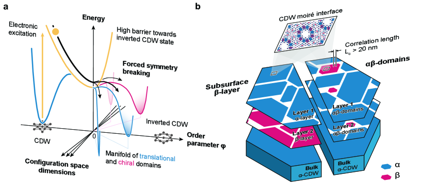
The ultrashort electronic enhancement and vibrationally coherent character of the hidden-state preparation Maklar2023 ; Ravnik2018 provides a hint to the generation mechanism, which we discuss with the illustration in Fig. 3a. First, the electronic excitation by the laser pulse drastically deforms the free-energy potential and induces a ballistic structural motion towards an inverted CDW state. Such an inverted state is energetically highly unfavorable and was reported to exhibit large upward band shifts Zhang2022 ; Maklar2023 . Thus, we propose that the subsequent ballistic evolution of the system beyond the high-symmetry state () and onto the high-energy barrier will cause a “forced symmetry breaking” (cf. Fig. 3a), as opposed to the spontaneous (Kibble-Zurek) symmetry breaking. As a result, the system locally branches off into many of the nearly degenerate configurations of the system. In this picture, the minority contribution of the chirality, as shown in our LEED images, can be attributed to its somewhat more unfavorable free energy and/or a narrower path across the transition state. The reversal to a monochiral state can also be understood on the basis of a shallow metastable energy minimum for a domain in an -domain environment.
Based on the present experimental evidence, we cannot assert with certainty the spatial distribution of generated domains. We carried out dynamical LEED simulations, which predict that only about 3.7 % of the total superstructure diffraction intensity stems from the subsurface layer (cf. Fig. S5c in the Supplementary Information). Therefore, in order to account for the observed 3-10 % of the total superstructure diffraction intensity contained in the peaks for different samples (Fig. 2b), a corresponding few-percentage minority of the surface layer (Fig. 3b, right) and/or a majority of the subsurface layer (Fig. 3b, left) will have to switch to the chirality. Recently, an STM study reported a state with mixed chiral domains after 1T-TaS2 crystals are exposed to a single laser pulse at a fluence of 3-5 mJ cm Ravnik2023 . This observation is in general agreement with the structural textures proposed here.
A full crystallographic reconstruction of the structure, as previously carried out for the homogeneous C-phase vonWitte2019 , is complicated by the intrinsic disorder of the hidden state. Specifically, we observe a reduced modulation of the energy-dependent LEED intensity (cf. Fig. S4b in the Supplementary Information) VanHove1986 , which likely follows from incoherent averaging over different stackings associated with translational nano-domains Gerasimenko2019 . Moreover, possible - cross peaks, which might be expected for a completely switched subsurface layer (Fig. 3b, left), are absent in our observations, which again suggests a surface layer of mixed -domains.
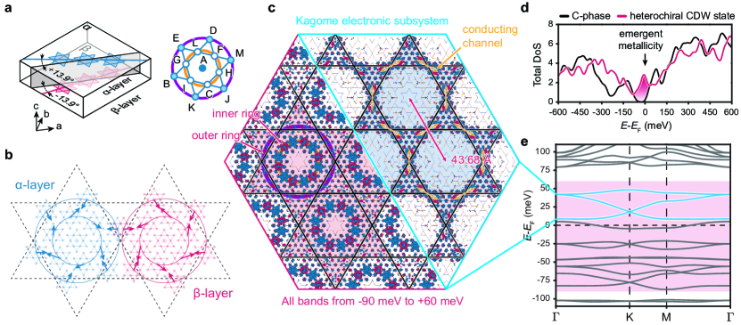
Irrespective of the specific details of the real-space texture, a general implication of our observations is the presence of extended interfaces of opposite CDW chirality at or near the surface, which causes the emergence of CDW moiré interfaces. In particular, the 27.8∘ rotational mismatch between CDWs in the and layers gives rise to a commensurate CDW moiré superstructure (cf. Fig. S6b in the Supplementary Information) with an unusually large moiré length () compared to typical large-angle moiré materials Shallcross2010 ; Tilak2023 ; Carr2020 . Using density functional theory (DFT) simulations, we explore the electronic and structural order of the CDW moiré interface, considering a simplified atomic structure composed of two 1T-TaS2 trilayers of opposite CDW chirality (Fig. 4a, left). The unit cell of the superstructure contains 13 Ta hexagrams in each trilayer, in a fractal-type arrangement that forms a "super-hexagram" (see also Fig. S6b). The angle between and super-hexagrams in adjacent layers creates a mixed stacking order Lee2019 (Fig. 4a, right). The periodically altering stacking is expected to lead to the collapse of interlayer dimerization Stahl2020 ; Ritschel2018 ; Lee2019 ; Petocchi2022 ; Nicholson2022 ; Salzmann2023 ; Lee2021 ; Butler2020 ; Fei2022 and locally varying conductivity, linking to the recent observation of the non-Drude-type conductivity of the hidden state Gao2022 .
The main results of our DFT simulations are summarized in Fig. 4b-e. In the CDW moiré unit cell (cf. Fig. S6b), the relaxed atomic structure transforms from a ()R13.9∘ triangular superlattice to a kagome superlattice (Fig. 4b and Fig. S7), with the CDW chirality and Ta hexagrams of each layer remaining unaltered. The atomic displacements are of the order . They collectively induce an electronic reconstruction, with electron density redistributed into a novel double-ring charge texture (Fig. 4c, left) with a charge-depleted central hexagram. A prominent inner charge ring is composed of 6 hexagrams, while a less pronounced outer ring spans 12 hexagrams shared by adjacent unit cells. This texture may arise from the stacking-dependent electrostatic energy, as discussed in Sec. III of the Supplementary Information. Such an electron density distribution may correspond to the ring-like charge structures observed by STM in Refs. Ohta2021 and Ravnik2023 , hence favoring the -domain texture (Fig. 3b, right). The regular domains observed in Ref. Ravnik2023 imply regions with a deeper heterochiral interface. We believe that future spectroscopic STM measurements will elucidate the connection between the observed ring-like charge pattern and the CDW moiré superstructure introduced here.
Alongside the structural transformation and electronic reconstruction, the density-of-states calculation shows an emergent conducting peak at the Fermi energy (), which strongly contrasts with the electronic gap of the C-phase (Fig. 4d and Fig. S9b). The band structure calculation further reveals multiple flat bands and Dirac cones emerging near (Fig. 4e). While the flat bands at may facilitate correlation effects Cao2018-1 ; Cao2018-2 , the lowest conduction bands (within 50 meV above ) feature characteristics of a kagome subsystem Yin2022 ; Dong2023 : a Dirac point at K, a Van Hove singularity at M and a flat band across -K-M-. The corresponding electron density distribution hosts a kagome network of conducting channels (Fig. 4c, right). It is worth noting that the nearly half-filled band at in Fig. 4d arises naturally from the heterochiral CDW lattice structure with the electronic reconstruction.
Conclusions
Combining femtosecond laser excitation with high-coherence LEED, we observe a heterochiral CDW state at the surface of 1T-TaS2 crystals, featuring laser-controlled reversibility, ultrafast electronic enhancement, and a threshold behavior. Prepared under conditions corresponding to the well-known hidden state in this material, we suggest that coexistent CDW chiralities are a structural feature closely linked to this state. Furthermore, we propose that this new structural element arises from an electronically-induced forced symmetry breaking. The coexistent long-range order of opposite charge-density wave chiralities implies the presence of extended heterochiral interfaces, either between the first two surface trilayers or up to few layers below the surface. Using DFT simulations, we reveal the electronic reconstruction of the double-ring charge texture, identify an emergent kagome system, and obtain a nearly half-filled band at . Future work may allow for large-area fabrication of CDW moiré interfaces. More broadly, our study demonstrates new possibilities for optical chiral engineering and light-induced moiré superstructures in quasi-two-dimensional materials.
Acknowledgements.
Acknowledgments
This work was funded by the European Research Council (ERC Starting Grant ‘ULEED’, ID: 639119, ERC Advanced Grant ‘ULEEM’, ID: 101055435), the Deutsche Forschungsgemeinschaft (SFB-1073, project A05) and ETH Zürich (ETH Postdoctoral Fellowship, J.G.H.). This work utilized high-performance computing clusters from the Holland Computing Center of the University of Nebraska, which receives support from the UNL Office of Research and Economic Development, and the Nebraska Research Initiative. H.-T.J. acknowledges support from NSTC, NCHC, CINC-NTU, AS-iMATE-111-12, and CQT-NTHU-MOE, Taiwan. W.C.H. gratefully acknowledges funding supports from NSTC 112-2811-M-001-007 and 113-2811-M-007-008. The authors thank Gero Storeck, Benjamin Schröder, Johannes Otto, Thomas Weitz, Matthias Krüger, and Jörg Malindretos for technical support and insightful discussions.
Author contributions
The project was conceived by C.R.; W.C.H. conducted experiments and data analysis with contributions from Y.S.L., F.K., and J.G.H; the 1T-TaS2 samples were provided by K.R.; S.M., S.-S.H., and H.-T.J. carried out the DFT simulations with contributions from W.C.H.; G.v.W. performed the dynamical LEED simulations; results of DFT and dynamical LEED simulations were analyzed by W.C.H., S.-S.H., H.-T.J., G.v.W., and S.M.; the manuscript was written by W.C.H. and C.R. with contributions from G.v.W, J.G.H., and F.K.. All authors discussed the results and commented on the manuscript.
I Methods
1. LEED measurements
In the experiments, large flakes of 1T-TaS2 samples (diameter 2-3 mm, thickness 150 m) are cleaved under high vacuum and transferred to an ultrahigh vacuum chamber with a base pressure of mbar. The samples are prepared in the C-phase at a temperature of 30 K using a liquid helium flow cryostat. LEED images in a backscattering geometry near normal incidence (cf. Fig. 1b) are recorded using a narrow electron beam (150 m diameter) with high momentum resolution from a millimeter-sized photoelectron gun (sample-to-gun distance 10 mm, see Ref. Vogelgesang2018 for details on the electron source). The low-temperature C-phase of 1T-TaS2 exhibits a ()R13.9∘ CDW superstructure. As our study is concerned with the chirality of the superstructure Zong2018 ; Ishioka2010 ; Song2022 ; Liu2023 , in each measurement, we begin with a large single-crystalline area of a single CDW chirality. The diffraction pattern of the initial state (cf. Fig. 1d, top-left panel) exhibits a hexagonal arrangement with bright main lattice peaks surrounded by weaker CDW superstructure peaks, which arise from the CDW-coupled periodic lattice distortion Overhauser1971 ; Eichberger2010 .
2. Electron-laser spatial overlap
We use single or double laser pulses to excite the sample under an angle of incidence of about 45 degrees. The laser spot size on the sample is 300 m (FWHM), ensuring uniform illumination of the area probed by the electron beam. The spatial overlap between the electron and laser beams is found using the technique of ultrafast low-energy electron diffraction (ULEED) Vogelgesang2018 . Specifically, at low-fluence excitation, we optimize the electron-laser overlap by maximizing the laser-induced Debye-Waller effect, i.e., the transient suppression of diffraction spot intensities.
3. Generation of single- and double-pulse
The optical quench of 1T-TaS2 samples is conducted using either single or double laser pulses. Single pulses are isolated with a Pockels cell inside a laser amplifier (center wavelength 1030 nm). Femtosecond excitation pulses of about 200 fs duration (center wavelength 800 nm, FWHM spectral width 7 nm) are produced by an optical parametric amplifier. Double pulses with a pulse separation are generated by passing a single pulse through a Michelson interferometer. A half-inch polarizing beamsplitter cube is used to split the pulse, and a quarter-wave plate is used in each arm of the interferometer to optimize the total laser power output. The two output pulses are orthogonally polarized with a measured interferometric visibility of 3 %.
4. Reversal from the heterochiral to the monochiral state
The duration of the annealing laser pulse train is controlled by a mechanical shutter that produces a 1 s top-hat function with rising and falling edges spanning about 10 ms. Given sufficient fluence, the annealing laser pulse train can completely reverse the heterochiral state to a monochiral state (cf. Fig. 2c). This procedure is used for initializing each measurement. Incomplete reversal was observed if a sharper drop of the pulse train envelope was used.
5. Density-functional theory simulations
Density functional theory (DFT) simulations are performed for the CDW moiré superstructure using projector augmented wave (PAW) Blochl1994 potentials as implemented in the Vienna Ab-initio Simulation Package (VASP) Kresse1993 ; Kresse1996 . A 350 eV kinetic energy cutoff in the plane-wave expansion is used. The PAW pseudopotentials correspond to the valence-electron configuration 5d36s2 for Ta and 3s23p4 for S. The exchange-correlation is treated within the generalized gradient approximation, as parameterized by Perdew, Burke, and Ernzerhof Perdew1996 . The Coulomb correlations within the 5d shells of Ta are described using the spherically averaged DFT+ method Dudarev1998 , where the Hamiltonian only depends on the difference between on-site interaction and Hund’s exchange , i.e., . We adopt the value of eV for the Ta 5d orbitals Darancet2014 . Spin-orbit coupling is ignored in all simulations Ritschel2018 . For structural relaxation, the lattice constants (13 times of the primitive cell lattice constant ) and (twice the Ta-Ta interlayer distance ) are fixed vonWitte2019 ; Spijkerman1997 ; Givens1977 , while the positions of 1014 atoms are relaxed by a -centered k-point mesh until the maximum force on each atom becomes less than 10 meV/Å. A -centered k-point mesh is used for calculating the self-consistent ground state charge and electronic band structures. The total energies are converged to 10 eV. In a separate calculation, The 1T-TaS2 C-phase is simulated by a 156-atom AL-stacking unit cell using a -centered k-point mesh Ritschel2018 ; Lee2019 .
References
- (1) C. Bao, P. Tang, D. Sun, and S. Zhou, Light-induced emergent phenomena in 2D materials and topological materials, Nat. Rev. Phys. 4, 33 (2022).
- (2) A. de la Torre, D. M. Kennes, M. Claassen, S. Gerber, J. W. McIver, and M. A. Sentef, Colloquium: Nonthermal pathways to ultrafast control in quantum materials, Rev. Mod. Phys. 93, 041002 (2021).
- (3) D. N. Basov, R. D. Averitt, and D. Hsieh, Towards properties on demand in quantum materials, Nat. Mater. 16, 1077 (2017).
- (4) L. Stojchevska, I. Vaskivskyi, T. Mertelj, P. Kusar, D. Svetin, S. Brazovskii, and D. Mihailovic, Ultrafast switching to a stable hidden quantum state in an electronic crystal, Science 344, 177 (2014).
- (5) J. G. Horstmann, H. Böckmann, B. Wit., F. Kurtz, G. Storeck, and C. Ropers, Coherent control of a surface structural phase transition, Nature 583, 232 (2020).
- (6) M. Rini, R. Tobey, N. Dean, J. Itatani, Y. Tomioka, Y. Tokura, R. W. Schoenlein, and A. Cavalleri, Control of the electronic phase of a manganite by mode-selective vibrational excitation, Nature 449, 72 (2007).
- (7) J. Maklar, J. Sarkar, S. Dong, Y. A. Gerasimenko, T. Pincelli, S. Beaulieu, P. S. Kirchmann, J. A. Sobota, S. Yang, D. Leuenberger, R. G. Moore, Z. -X. Shen, M. Wolf, D. Mihailovic, R. Ernstorfer, and L. Rettig , Coherent light control of a metastable hidden state, Sci. Adv. 9, eadi4661 (2023).
- (8) M. Hase, P. Fons, K. Mitrofanov, A. V. Kolobov, and J. Tominaga, Femtosecond structural transformation of phase-change materials far from equilibrium monitored by coherent phonons, Nat. Commun. 6, 8367 (2015).
- (9) A. M. Weiner, D. E. Leaird, G. P. Wiederrecht, and K. A. Nelson, Femtosecond pulse sequences used for optical manipulation of molecular motion, Science 247, 1317 (1990).
- (10) I. Vaskivskyi, I.A. Mihailovic, S. Brazovskii, J. Gospodaric, T. Mertelj, D. Svetin, P. Sutar, and D. Mihailovic, Fast electronic resistance switching involving hidden charge density wave states, Nat. Commun. 7, 11442 (2016).
- (11) F. Y. Gao, Z. Zhang, Z. Sun, L. Ye, Y. -H. Cheng, Z. -J. Liu, J. G. Checkelsky, E. Baldini, and K. A. Nelson, Snapshots of a light-induced metastable hidden phase driven by the collapse of charge order, Sci. Adv. 8, eabp9076 (2022).
- (12) D. Svetin, I. Vaskivskyi, S. Brazovskii, and D. Mihailovic, Three-dimensional resistivity and switching between correlated electronic states in 1T-TaS2, Sci. Rep. 7, 46048 (2017).
- (13) G. von Witte, T. Kißlinger, J. G. Horstmann, K. Rossnagel, M. A. Schneider, C. Ropers, and L. Hammer, Surface structure and stacking of the commensurate ()R13.9∘ charge density wave phase of 1T-TaS2(0001), Phys. Rev. B 100, 155407 (2019).
- (14) L. Ma, C. Ye, Y. Yu, X. F. Lu, X. Niu, S. Kim, D. Feng, D. Tománek, Y. -W. Son, X. H. Chen, and Y. Zhang, A metallic mosaic phase and the origin of Mott-insulating state in 1T-TaS2, Nat. Commun. 7, 10956 (2016).
- (15) D. Cho, S. Cheon, K. -S. Kim, S. -H. Lee, Y. -H. Cho, S. -W. Cheong, and H. W. Yeom, Nanoscale manipulation of the Mott insulating state coupled to charge order in 1T-TaS2, Nat. Commun. 7, 10453 (2016).
- (16) Y. A. Gerasimenko, P. Karpov, I. Vaskivskyi, S. Brazovskii, and D. Mihailovic, Intertwined chiral charge orders and topological stabilization of the light-induced state of a prototypical transition metal dichalcogenide, npj Quantum Mater. 4, 32 (2019).
- (17) I. Vaskivskyi, J. Gospodaric, S. Brazovskii, D. Svetin, P. Sutar, E. Goreshnik, I. A. Mihailovic, T. Mertelj, and D. Mihailovic, Controlling the metal-to-insulator relaxation of the metastable hidden quantum state in 1T-TaS2, Sci. Adv. 1, e1500168 (2015).
- (18) Q. Stahl, M. Kusch, F. Heinsch, G. Garbarino, N. Kretzschmar, K. Hanff, K. Rossnagel, J. Geck, and T. Ritsche, Collapse of layer dimerization in the photo-induced hidden state of 1T-TaS2, Nat. Commun. 11, 1247 (2020).
- (19) S. Vogelgesang, G. Storeck, J. G. Horstmann, T. Diekmann, M. Sivis, S. Schramm, K. Rossnagel, S. Schäfer, and C. Ropers, Phase ordering of charge density waves traced by ultrafast low-energy electron diffraction, Nat. Phys. 14, 185 (2018).
- (20) J. Ravnik, I. Vaskivskyi, T. Mertelj, and D. Mihailovic, Real-time observation of the coherent transition to a metastable emergent state in 1T-TaS2, Phys. Rev. B 97, 075304 (2018).
- (21) X. Song, L. Liu, Y. Chen, H. Yang, Z. Huang, B. Hou, Y. Hou, X. Han, H. Yang, Q. Zhang, T. Zhang, J. Zhou, Y. Huang, Y. Zhang, H. -J. Gao, and Y. Wang, Atomic-scale visualization of chiral charge density wave superlattices and their reversible switching, Nat. Commun. 13, 1843 (2022).
- (22) L. Liu, X. Song, J. Dai, H. Yang, Y. Chen, X. Huang, Z. Huang, H. Ji, Y. Zhang, X. Wu, J. -T. Sun, Q. Zhang, J. Zhou, Y. Huang, J. Qiao, W. Ji, H. -J. Gao, and Y. Wang, Unveiling electronic behaviors in heterochiral charge-density-wave twisted stacking materials with 1.25 nm unit dependence, ACS Nano 17, 2702 (2023).
- (23) S. Ohta, S. Kobayashi, A. Nomura, and H. Sakata, Electronic state modulation of the Star of David lattice by stacking of domains in 1T-TaSe2, Phys. Rev. B 104, 155433 (2021).
- (24) L. Stojchevska, P. Šutar, E. Goreshnik, D. Milhailovic, and T. Mertelj, Stability of the light-induced hidden charge density wave state within the phase diagram of 1T-TaSSe, Phys. Rev. B 98, 195121 (2018).
- (25) A. Zong, X. Shen, A. Kogar, L. Ye, C. Marks, D. Chowdhury, T. Rohwer, B. Freelon, S. Weathersby, R. Li, J. Yang, J. Checkelsky, X. Wang, and N. Gedik, Ultrafast manipulation of mirror domain walls in a charge density wave, Sci. Adv. 4, eaau5501 (2018).
- (26) S. Vogelgesang, Ultrafast low-energy electron diffraction at surfaces, PhD Thesis, University of Göttingen (2018).
- (27) G. Storeck, J. G. Horstmann, T. Diekmann, S. Vogelgesang, G. von Witte, S. V. Yalunin, K. Rossnagel, and C. Ropers, Structural dynamics of incommensurate charge-density waves tracked by ultrafast low-energy electron diffraction, Struct. Dyn. 7, 034304 (2020).
- (28) G. Storeck, K. Rossnagel, and C. Ropers, Ultrafast spot-profile LEED of a charge-density wave phase transition, Appl. Phys. Lett. 118, 221603 (2021).
- (29) S. Deutschländer, P. Dillmann, G. Maret, and P. Keim, Kibble-Zurek mechanism in colloidal monolayers, PNAS 112, 6925 (2015).
- (30) T. Eggebrecht, M. Möller, J. G. Gatzmaan. N. R. da Silva, A. Feist, U. Martens, H. Ulrichs, M. Münzenberg, C. Ropers, and S. Schäfer, Light-induced metastable magnetic texture uncovered by in situ Lorentz microscopy, Phys. Rev. Lett. 118, 097203 (2017).
- (31) Y. Zhang, X. Shi, M. Guan, W. You, Y. Zhong, T. R. Kafle, Y. Huang, H. Ding, M. Bauer, K. Rossnagel, S. Meng, H. C. Kapteyn, and M. M. Murnane, Creation of a novel inverted charge density wave state, Struct. Dyn. 9, 014501 (2022).
- (32) J. Ravnik, J. Vodeb, Y. Vaskivskyi, M. Diego, R. Venturini, Y. Gerasimenko, V. Kabanov, A. Kranjec, and D. Mihailovic, Chiral domain dynamics and transient interferences of mirrored superlattices in nonequilibrium electronic crystals, Sci. Rep. 13, 19622 (2023).
- (33) M. A. Van Hove, W. H. Weinberg, and C. -M. Chan, Low-Energy Electron Diffraction, (Springer, Berlin, 1986).
- (34) S. Shallcross, S. Sharma, E. Kandelaki, and O. A. Pankratov, Electronic structure of turbostratic graphene, Phys. Rev. B 81, 1 (2010).
- (35) N. Tilak, M. Altvater, S. -H. Hung, C. -J. Won, G. Li, T. Kaleem, S. -W. Cheong, C. -H. Chung, H. -T. Jeng, and E. Y. Andrei, Revealing the charge density wave proximity effect in graphene on 1T-TaS2, arXiv:2311.10606 (2023).
- (36) S. Carr, S. Fang, and E. Kaxiras, Electronic-structure methods for twisted moiré layers, Nat. Rev. Mater. 5, 749 (2020).
- (37) S. -H. Lee, J. S. Goh, and D. Cho, Origin of the insulating phase and first-order metal-insulator transition in 1T-TaS2, Phys. Rev. Lett. 122, 106404 (2019).
- (38) T. Ritschel, H. Berger, and J. Geck, Stacking-driven gap formation in layered 1T-TaS2, Phys. Rev. B 98, 195134 (2018).
- (39) C. W. Nicholson, F. Petocchi, B. Salzmann, C. Witteveen, M. Rumo, G. Kremer, F. O. von Rohr, P. Werner, and C. Monney, Modified interlayer stacking and insulator to correlated-metal transition driven by uniaxial strain in 1T-TaS2, arXiv:2204.05598 (2022).
- (40) B. Salzmann, E. Hujala, C. Witteveen, B. Hildebrand, H. Berger, F. O. von Rohr, C. W. Nicholson, and C. Monney, Observation of the metallic mosaic phase in 1T-TaS2 at equilibrium, Phys. Rev. Mater. 7, 064005 (2023).
- (41) C. J. Butler, M. Yoshida, T. Hanaguri, and Y. Iwasa, Mottness versus unit-cell doubling as the driver of the insulating state in 1T-TaS2, Nat. Commun. 11, 2477 (2020).
- (42) J. Lee, K. -H. Jin, and H. W. Yeom, Distinguishing a Mott Insulator from a trivial insulator with atomic adsorbates, Phys. Rev. Lett. 126, 196405 (2021).
- (43) F. Petocchi, C. W. Nicholson, B. Salzmann, D. Pasquier, O. V. Yazyev, C. Monney, and P. Werner, Mott versus hybridization gap in the low-temperature phase of 1T-TaS2, Phys. Rev. Lett. 129, 016402 (2022).
- (44) Y. Fei, Z. Wu, W. Zhang, and Y. Yin, Understanding the Mott insulating state in 1T-TaS2 and 1T-TaSe2, AAPPS Bull. 32, 20 (2022).
- (45) Y. Cao, V. Fatemi, S. Fang, K. Watanabe, T. Taniguchi, E. Kaxiras, and P. Jarillo-Herrero, Unconventional superconductivity in magic-angle graphene superlattices, Nature 556, 43 (2018).
- (46) Y. Cao, V. Fatemi, A. Demir, S. Fang, S. L. Tomarken, J. Y. Luo, J. D. Sanchez-Yamagishi, K. Watanabe, T. Taniguchi, E. Kaxiras, R. C. Ashoori, P. Jarillo-Herrero, Correlated insulator behaviour at half-filling in magic-angle graphene superlattices, Nature 556, 80 (2018).
- (47) J. -X. Yin, B. Lian, and M. Z. Hasan, Topological kagome magnets and superconductors, Nature 612, 647 (2022).
- (48) H. Dong, P. Sun, L. Lei, Y. Geng, J. Guo, Y. Li, L. Huang, R. Xu, F. Pang, W. Ji, W. Zhou, Z. Liu, Z. -Y. Lu, H. -J. Gao, K. Liu, and Z. Cheng, Emergent electronic kagome lattice in correlated charge-density-wave state of 1T-TaS2, arXiv:2301.05885 (2023).
- (49) J. Ishioka, Y. H. Liu, K. Shimatake, T. Kurosawa, K. Ichimura, Y. Toda, M. Oda, and S. Tanda, Chiral charge-density waves, Phys. Rev. Lett. 105, 176401 (2010).
- (50) A. Overhauser, Observability of charge-density waves by neutron diffraction, Phys. Rev. B 10, 3173 (1971).
- (51) M. Eichberger, H. Schäfer, M. Krumova, M. Beyer, J. Demsar, H. Berger, G. Moriena, G. Sciaini, and R. J. D. Miller, Snapshots of cooperative atomic motions in the optical suppression of charge density waves, Nature 468, 799 (2010).
- (52) P. E. Blöchl, Projector augmented-wave method, Phys. Rev. B 50, 17953 (1994).
- (53) G. Kresse and J. Hafner, Ab initio molecular dynamics for liquid metals, Phys. Rev. B 47, 558 (1993).
- (54) G. Kresse and J. Furthmüller, Efficient iterative schemes for ab initio total-energy calculations using a plane-wave basis set, Phys. Rev. B 54, 11169 (1996).
- (55) J. P. Perdew, K. Burke, and M. Ernzerhof, Generalized Gradient Approximation Made Simple, Phys. Rev. Lett. 77, 3865 (1996).
- (56) S. L. Dudarev, G. A. Botton, S. Y. Savrasov, C. J. Humphreys, and A. P. Sutton, Electron-energy-loss spectra and the structural stability of nickel oxide: An LSDA+U study, Phys. Rev. B 57, 1505 (1998).
- (57) P. Darancet, A. J. Millis, and C. A. Marianetti, Three-dimensional metallic and two-dimensional insulating behavior in octahedral tantalum dichalcogenides, Phys. Rev. B 90, 045134 (2014).
- (58) A. Spijkerman, J. L. de Boer, A. Meetsma, and G. A. Wiegers, X-ray crystal-structure refinement of the nearly commensurate phase of 1T-TaS2 in (3+2)-dimensional superspace, Phys. Rev. B 56, 13757 (1997).
- (59) F. Givens and G. Fredericks, Thermal expansion of NbSe2 and TaS2, J. Phys. Chem. Solids 38, 1363 (1977).