Detection of Low-Energy Electrons with Transition-Edge Sensors
Abstract
We present the first detection of electrons with kinetic energy in the 100 eV range with transition-edge sensors (TESs). This has been achieved with a m2 Ti-Au bilayer TES, with a critical temperature of about 84 mK. The electrons are produced directly in the cryostat by a cold-cathode source based on field emission from vertically-aligned multiwall carbon nanotubes. We obtain a Gaussian energy resolution between 0.8 and 1.8 eV for fully-absorbed electrons in the eV energy range, which is found to be compatible with the resolution of this same device for photons in the same energy range. This measurement opens new possibilities in the field of electron detection.
Transition-edge sensors (TESs) are highly sensitive micro-calorimeters capable of high-resolution single-photon counting across a wide energy spectrum Irwin (1995); Cunningham et al. (2002). The detection scheme is based on the absorption of the incoming photons in a thin superconducting film, in which their energy is transformed into heat. By operating a TES device at its critical temperature , even small variations in temperature lead to measurable changes in its electrical resistance, owing to the steep transition between the superconducting regime and the normal-conduction one. TES devices have been capable of achieving single-photon Gaussian energy resolutions below 50 meV for 0.8 eV photons Hattori et al. (2022); Lolli et al. (2013).
In principle, this detection scheme should also be sensitive to low-energy electrons absorbed in the superconducting film, as seems to be confirmed by simulations Patel et al. (2021). However, there is currently very limited research on the use of TES devices for electron detection, except for a recent unpublished result on keV electrons Patel et al. (2024). Low-energy electrons have been detected with other detection schemes, such as micro-channel plates Apponi et al. (2022a), which have only very poor energy resolution, and also feature geometrical inefficiencies due to their non-unitary fill factor; and silicon detectors, such as avalanche photo-diodes Apponi et al. (2020) and silicon drift detectors Gugiatti et al. (2020), which are characterized by the presence of a dead layer at the detector entrance, in which low-energy electrons are absorbed before generating a signal. On the other hand TES devices offer, in principle, a detection scheme without dead layers and with unitary fill factor, therefore with the potential for high efficiency and excellent intrinsic energy resolution on low-energy electrons. This would be of great interest for a wide range of experiments, such as, for example, the PTOLEMY project Betti et al. (2019a, b); Apponi et al. (2022b), which plans to search for the cosmic neutrino background by analyzing the endpoint of the beta decay of tritium with unprecedented electron energy resolution.

In this work, electrons are produced by field emission from vertically-aligned, multi-wall carbon nanotubes (CNTs). This ‘cold-cathode source’ solution overcomes the issues in interfacing standard hot-filament-based electron sources with the TES working at cryogenic temperature, thus allowing to place the source directly inside the cryostat close to the TES. The results presented here were obtained in the Innovative Cryogenic Detectors Laboratory of Istituto Nazionale di Ricerca Metrologica (INRiM) in Torino (Italy) Pepe (2023). The TES detectors operate on the 30 mK stage of an adiabatic demagnetization refrigerator cryostat. Since electrons in motion are affected by magnetic fields, and TESs and DC-SQUIDs are also sensitive to magnetic fields, a cryogenic magnetic shield was installed within the cryostat around the working area to suppress any magnetic interference that could degrade the sensor performance and alter electron trajectories.
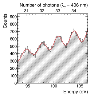
A schematic view of the experimental setup is shown in Figure 1: a cross section of the layers which compose the TES and the shield is shown in panel (a), while panel (b) shows a schematic 3D model of it. The TES device used in this work was fabricated at QR Lab, INRiM, has an area of , and is a Ti-Au bilayer device, composed of a 15 nm layer of titanium covered by a 30 nm layer of gold, deposited by thermal evaporation on a 500 nm silicon nitride substrate Monticone et al. (2021). It is wired with 50 nm superconducting Nb strips, which were deposited on the substrate via sputtering. The TES has a critical temperature mK and was characterized in the eV energy range with 406 nm photons from a pulsed laser. The result of this characterization, in the energy range of interest for this work, is shown in Figure 2: the peaks corresponding to a number of photons , 32, 33, and 34 are clearly distinguishable, and fitted with a sum of Gaussian functions.
This TES design was adapted for electron detection by adding a shield layer, which is needed as the electron source has a significantly larger area (approximately mm2) compared to the TES active area ( m2). The shield leaves the TES active area exposed, but covers the area surrounding it, specifically the Nb wiring and the substrate, as direct electron hits on the wiring would induce electrical noise, while on the insulating substrate would lead to charge build-up. The shield layer is produced by thermal evaporation, depositing an insulating layer consisting of 300 nm of amorphous silicon oxide (SiOx) Monticone et al. (2000), followed by a thin (5 nm) layer of titanium, and finally a 50 nm layer of gold. The thin titanium layer is necessary for best adhesion of gold to the SiOx.
The electron source consists of a sample of CNTs which were synthesized in the INFN laboratory ‘TITAN’ at Sapienza University of Rome Schifano et al. (2023); Yadav et al. (2024); Sarasini et al. (2022); Tayyab et al. (2024). The nanotubes were grown through chemical vapor deposition on a 500 m silicon substrate, and are approximately 200 m in length, while covering a surface of roughly mm2. Thanks to the high geometrical field enhancement factor of their tips, nanotubes are capable of emitting electrons through quantum tunneling (field emission) without the necessity of applying very high voltages de Heer et al. (1995); Lahiri and Choi (2011); Semet et al. (2002); Lin et al. (2015). Furthermore, as this emission is quantic in nature, and not thermal, it does not generate heat and can therefore be used in a cryostat. Moreover, within the energy range under consideration, we can assume that this source is monochromatic: the energy spread of the emitted electrons, in fact, is expected to be of the order of , which at cryogenic temperatures is only a few eV.
The TES and the nanotubes were placed on two copper plates, facing each other, separated by 0.5 mm sapphire spacers, which ensure electrical insulation while guaranteeing a good degree of thermal conductance. The top copper plate, where the nanotubes are hosted, was connected to a power supply, and was provided negative voltage in order to produce field-emission electrons; the bottom plate was put in thermal contact with the cryostat, and grounded electrically through it. The distance between the tips of the nanotubes and the surface of the TES, in this setup, was mm. A schematic view of the setup is shown in panel (c) of Figure 1.
The electron emission from the CNTs was read-out in two different ways. In the ‘anode’ configuration the TES was short-circuited to the metallic shield layer, and the two were used as a large-area metallic plate sensitive to the full electron current emitted by the CNTs by connecting it to a Keithley 6487 picoammeter. In the ‘counting’ configuration the TES output was sensitive to single-particle absorption. This was achieved by voltage biasing the TES to its critical temperature via electrothermal feedback Irwin (1995). The TES working point was chosen to be , where is the resistance of the TES in normal state. The TES was read-out with a DC-SQUID transimpedence amplifier Drung et al. (2007).
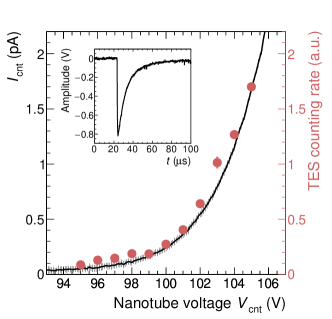
The results in the anode configuration are summarized by the black curve of Figure 3, where the current emitted by the nanotubes is shown as a function of . As can be seen, exhibits an exponential rise, compatible with the Fowler-Nordheim theory on field emission Fowler and Nordheim (1928). Superimposed on the same plot with red markers is the rate of counts recorded by the TES in counting mode. As can be seen the increase in counting rate as a function of follows the same exponential rise as , therefore proving that the signals recorded by the TES are due to electrons. The inset in Figure 3 shows a typical TES signal for V, characterized by a very fast rise time ns, and a recovery time s.
A feature of Fowler-Nordheim emission is that the current of emitted electrons by the nanotubes depends on the electric field in proximity of their tips, which in our planar configuration corresponds, in first approximation, to . At the same time, if we assume that electrons are emitted by the nanotubes with zero initial kinetic energy, also determines the kinetic energy of the electrons when entering the TES. Therefore, in this setup, the signal rate and electron energy are not independent parameters, as they both depend on .
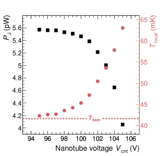
The electrons are emitted from a relatively large area compared to the TES, and the additional heating created by the electrons hitting its nearby environment must be considered. When the CNTs are off () or at low , the electron rate and the energy deposited are minimal, keeping the temperature of the area around the TES at the cryostat bath temperature ( mK). In this condition, the Joule power required to bring the TES to its critical temperature is given by . For this device, the exponential parameter was found to be and the coupling constant W.
However, as increases, the rate of electrons and the associated energy deposition in the vicinity of the TES increase, raising the local temperature above the bath temperature. As a result, the local temperature becomes higher than and closer to . Consequently, less is needed to bring the TES to its working point at the critical temperature. This effect is shown in Figure 4, where the black markers represent the power needed to bring the TES to its nominal working point, and it can be seen that this power decreases as increases. The reduction of the dissipated power is interpreted as an increase in the local temperature of the area in direct contact with the TES, shown with red markers in Figure 4. When operating the electron source at V, the local temperature is already higher than 60 mK, compared to the initial temperature of about 41 mK before electron emission. This implies that results at different values are not rigorously comparable, as the TES operates under slightly different conditions.
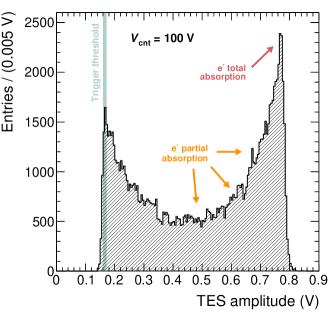
For each value of , the amplitude of the signals produced by the TES were analyzed. A typical spectrum, obtained for V is shown in Figure 5: as can be seen the distribution presents a high-amplitude peak, corresponding to the full absorption of the electron energy in the sensitive layer of the TES; a marked tail to the left of the peak, due to partial absorption of electrons, and is most likely due to non-containment in the thickness of the device, as the TES bilayer is very thin (45 nm); and a low-amplitude peak, truncated by the trigger threshold of 166 mV, compatible with electrons back-scattered out of the TES after exciting an internal mode in the Au layer.
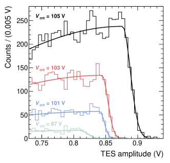
We fit the high-amplitude peaks of these distributions with an asymmetric Gaussian function, described by its peak position and its left () and right () tails. Some example fits, for , 101, 103, and 105 V, are shown in Figure 6.
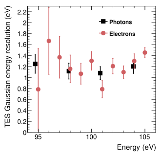
Figure 7 shows the TES Gaussian energy resolution for electrons (red circular markers) and photons (black square markers) as a function of the incoming particle energy. The electron energy resolution is defined as , where , where is the Coulomb charge and is the charge of the electron. The parameter describes the broadness of the high-energy tail of the absorption peak in the TES amplitude distribution. While the left tail is dominated by electron non-containment effects, the right tail is dominated by the energy resolution of the device, plus negligible effects due to the non-monochromaticity of the source. The photon energy resolution is instead obtained from the characterization shown in Figure 2. As can be seen, there is no significant difference in TES energy resolution between electrons and photons in this energy range. The electron Gaussian resolution, in particular, is measured to be eV for electrons in the eV energy range.
To conclude, this work reports the detection of low-energy electrons with a transition-edge sensor device. This has been achieved with the use of a cold electron source, based on field emission from vertically-aligned carbon nanotubes. We achieved a Gaussian energy resolution between 0.8 and 1.8 eV for fully-contained electrons in the eV energy range. Notably, this resolution is comparable to the energy resolution of the same TES device for photons in the same energy range, demonstrating for the first time a direct comparison between photon and electron energy resolutions. This work, together with Patel et al. (2024), open new possibilities in the detection of electrons, as they represent the first detection of such particles with intrinsic energy resolution without using electrostatic analyzers (as currently done in electron spectroscopy Boumsellek et al. (1990)), and with no form of particle multiplication (such as the case of ionization-based devices). TES devices, furthermore, have no dead layers and are therefore capable of excellent energy resolution, as proved by this work.
I Acknowledgements
The authors are grateful to Elio Bertacco, Martina Marzano, Matteo Fretto and Ivan De Carlo for technical support, as well as the PTOLEMY collaboration for useful discussions. This research was partially funded by the contribution of grant 62313 from the John Templeton Foundation, by PRIN grant ‘ANDROMeDa’ (PRIN_2020Y2JMP5) of Ministero dell’Università e della Ricerca, and from the EC project ATTRACT (Grant Agreement No. 777222).
References
- Irwin (1995) K. Irwin, Applied Physics Letters 66, 1998 (1995).
- Cunningham et al. (2002) M. Cunningham, J. Ullom, T. Miyazaki, S. Labov, J. Clarke, T. Lanting, A. T. Lee, P. Richards, J. Yoon, and H. Spieler, Applied Physics Letters 81, 159 (2002).
- Hattori et al. (2022) K. Hattori, T. Konno, Y. Miura, S. Takasu, and D. Fukuda, Superconductor Science and Technology 35, 095002 (2022).
- Lolli et al. (2013) L. Lolli, E. Taralli, C. Portesi, E. Monticone, and M. Rajteri, Applied Physics Letters 103, 041107 (2013).
- Patel et al. (2021) K. Patel, S. Withington, C. Thomas, D. Goldie, and A. Shard, Superconductor Science and Technology 34, 125007 (2021).
- Patel et al. (2024) K. Patel, S. Withington, A. Shard, D. Goldie, and C. Thomas, arXiv preprint arXiv:2403.01160 (2024).
- Apponi et al. (2022a) A. Apponi, F. Pandolfi, I. Rago, G. Cavoto, C. Mariani, and A. Ruocco, Measur. Sci. Tech. 33, 025102 (2022a).
- Apponi et al. (2020) A. Apponi, G. Cavoto, M. Iannone, C. Mariani, F. Pandolfi, D. Paoloni, I. Rago, and A. Ruocco, JINST 15, P11015 (2020).
- Gugiatti et al. (2020) M. Gugiatti, M. Biassoni, M. Carminati, O. Cremonesi, C. Fiorini, P. King, P. Lechner, S. Mertens, L. Pagnanini, M. Pavan, and S. Pozzi, Nuclear Instruments and Methods in Physics Research Section A: Accelerators, Spectrometers, Detectors and Associated Equipment 979, 164474 (2020).
- Betti et al. (2019a) M. G. Betti et al. (PTOLEMY Collaboration), Prog. Part. Nucl. Phys. 106, 120 (2019a).
- Betti et al. (2019b) M. G. Betti et al. (PTOLEMY Collaboration), Journal of Cosmology and Astroparticle Physics 2019, 047 (2019b).
- Apponi et al. (2022b) A. Apponi et al. (PTOLEMY Collaboration), Journal of Instrumentation 17, P05021 (2022b).
- Pepe (2023) C. Pepe, Nuovo Cimento C 46, 75 (2023).
- Monticone et al. (2021) E. Monticone, M. Castellino, R. Rocci, and M. Rajteri, IEEE Transactions on Applied Superconductivity 31, 1 (2021).
- Monticone et al. (2000) E. Monticone, A. M. Rossi, M. Rajteri, R. S. Gonnelli, V. Lacquaniti, and G. Amato, Philosophical Magazine B 80, 523 (2000).
- Schifano et al. (2023) E. Schifano, G. Cavoto, F. Pandolfi, G. Pettinari, A. Apponi, A. Ruocco, D. Uccelletti, and I. Rago, Nanomaterials 13, 1081 (2023).
- Yadav et al. (2024) R. P. Yadav, I. Rago, F. Pandolfi, C. Mariani, A. Ruocco, S. Tayyab, A. Apponi, and G. Cavoto, Nuclear Instruments and Methods in Physics Research Section A: Accelerators, Spectrometers, Detectors and Associated Equipment 1060, 169081 (2024).
- Sarasini et al. (2022) F. Sarasini, J. Tirillò, M. Lilli, M. P. Bracciale, P. E. Vullum, F. Berto, G. De Bellis, A. Tamburrano, G. Cavoto, F. Pandolfi, and I. Rago, Composites Part B: Engineering 243, 110136 (2022).
- Tayyab et al. (2024) S. Tayyab, A. Apponi, M. G. Betti, E. Blundo, G. Cavoto, R. Frisenda, N. Jiménez-Arévalo, C. Mariani, F. Pandolfi, A. Polimeni, et al., Nanomaterials 14, 77 (2024).
- de Heer et al. (1995) W. A. de Heer, A. Châtelain, and D. Ugarte, Science 270, 1179 (1995).
- Lahiri and Choi (2011) I. Lahiri and W. Choi, Acta Materialia 59, 5411 (2011).
- Semet et al. (2002) V. Semet, V. T. Binh, P. Vincent, D. Guillot, K. Teo, M. Chhowalla, G. Amaratunga, W. Milne, P. Legagneux, and D. Pribat, Applied Physics Letters 81, 343 (2002).
- Lin et al. (2015) P.-H. Lin, C.-L. Sie, C.-A. Chen, H.-C. Chang, Y.-T. Shih, H.-Y. Chang, W.-J. Su, and K.-Y. Lee, Nanoscale research letters 10, 1 (2015).
- Drung et al. (2007) D. Drung, C. Abmann, J. Beyer, A. Kirste, M. Peters, F. Ruede, and T. Schurig, IEEE Transactions on Applied Superconductivity 17, 699 (2007).
- Fowler and Nordheim (1928) R. H. Fowler and L. Nordheim, Proceedings of the Royal Society of London. Series A, Containing Papers of a Mathematical and Physical Character 119, 173 (1928).
- Boumsellek et al. (1990) S. Boumsellek, V. N. Tuan, and V. Esaulov, Review of scientific instruments 61, 1854 (1990).