2D hydrodynamic simulation of TeraFETs beyond the gradual-channel approximation for transient, large-signal or ultrahigh-frequency simulations
In the past decade, detection of THz radiation by plasma-wave-assisted frequency mixing in antenna-coupled field-effect transistors (TeraFETs) – implemented in various semiconductor material systems (Si CMOS, GaN/AlGaN, GaAs/AlGaAs, graphene, etc.) – has matured and led to a practically applied detector technology. This has been supported by the development of powerful device simulation tools which take into account relevant collective carrier dynamics and mixing processes in various approximations. These tools mostly model carrier transport in 1D and they are usually geared towards continuous-wave illumination of the device and small-signal response. Depending on their implementation, it may not be possible readily to simulate large-signal and pulsed operation. Another approximation which may lead to unsatisfactory results is the 1D restriction to calculate only the longitudinal electric field components. Especially at the edges of the gate electrode, solving of the 2D Poisson equation promises better results. This contribution introduces a stable way to solve the 2D Poisson equation self-consistently with the hydrodynamic transport equations including the numerically challenging convection term. We employ a well-balanced approximate Harten-Lax-van-Leer-Contact Riemann solver. The approach is well suited for a future treatment of transient and large-signal cases as well as the Dyakonov-Shur instability. The 2D treatment also generically extends the model beyond the gradual-channel approximation and allows to calculate the FET’s response at high THz frequencies where the gate-to-channel potential acquires a non-local character. Model calculations are performed for the exemplary case of a 65-nm Si CMOS TeraFET in the isothermal approximation.
Keywords TCAD, hydrodynamic, modeling, HLLC, Riemann solver, Si, CMOS, MOSFET, plasma wave, terahertz detection
1 Introduction
Three decades ago, Dyakonov and Shur put forth the idea to use field-effect transistors (FETs) as resonators for plasma waves [1]. In their pioneering theoretical work they predicted that a steady current flow can become unstable against generation of gated quasi-two-dimensional (quasi-2D) plasma waves (plasmons) – this phenomenon being known as Dyakonov-Shur instability [2, 3, 4] and predicted to be a possible source of high-frequency electromagnetic radiation. In a follow-up work by the same authors, it was shown that the nonlinear mixing properties of the gated 2D plasmons can be used to detect and frequency-mix THz radiation in the FET channel [5]. The mathematical basis for their predications was a small-signal harmonic analysis of a reduced 1D hydrodynamic transport model (HDM), which neglected carrier diffusion, carrier heating and the embedding of the gated channel in a real circuit environment [6]. While no unambiguous experimental evidence for the Dyakonov-Shur instability has been found until now [7], antenna-coupled FETs (TeraFETs) are successfully in use as sensitive detectors and mixers [8, 9, 10, 11, 12, 13, 14, 15]. TeraFETs are implemented in various material systems and device technologies such as Si CMOS [6, 16, 17], III-V semiconductor-based high electron mobility transistors (HEMTs)[18, 19, 20, 21] and graphene FETs [22, 23, 24, 25]. TeraFETs are implemented with narrow-band or broadband antennae, have a detection speed in the sub-ns range [26] and exhibit high sensitivity with values of the optical noise equivalent power (NEP) as low as 20 pW/Hz [27, 25] at room temperature. That gated plasmons can be excited in TeraFETs by THz radiation has been confirmed by both transport measurements [28, 29, 30] and s-SNOM experiments [31].
The response of TeraFETs to continuous-wave THz radiation in the small-signal limit can be simulated on the basis of a 1D HDM, often in the form of an equivalent waveguide representation which can be embedded into a circuit design tool [32, 33]. The small-signal THz transport processes can also be captured empirically, e.g. by means of a Volterra series approach [34]. Quantitative agreement with the measured responsivity and NEP values is achieved. However, the models are not suitable to treat transient phenomena upon pulsed THz excitation, to determine the large-signal response, or to correctly describe the detector response at very high THz frequencies (above 10 THz). In order to find a way to extend the HDM modeling to such cases, we will have a closer look at the challenges which arise if the usual approximations are lifted.
The HDM consists of a set of equations associated with conservation laws. These equations can be derived from the Boltzmann transport equation using the method of moments [35, 36]. The two main moments-based transport models are the Drift-Diffusion (DD) and the Energy-Balance (EB) model, which account for two and three moments of the charge carriers’ distribution functions, respectively. Both models contain a spatial derivative of the kinetic energy of the charge carriers which for strong spatial electric field gradients gives rise to a convective response of the carrier ensemble. The numerical treatment of convection is challenging and may not converge, with the risk increasing with the number of dimensions taken into account. For this reason, implementations of the models in commercially available computer-aided design software (e.g. from the companies Synopsys or Silvaco) neglect the convection term (unlike 1D treatments such as those in [37, 38, 33]). This approximation is often referred to as the diffusion approximation [36]. Mathematically, the resulting equation systems form a parabolic system of partial differential equations (PDEs). They can be solved numerically by means of well-known Scharfetter-Gummel (SG) discretization schemes [39, 40]. DD and EB models in the diffusion approximation have become a backbone for the simulation of device physics of modern transistor technology. While they also allow for the simulation of TeraFETs at low THz frequencies (e.g., 0.3 THz, simulated using the Sentaurus model of Synopsys [41]), it is expected that these simulations will deviate from experimental results as the excitation frequency is increased and plasma waves become important [36, 32, 42, 33].
Mathematically, the inclusion of the convection term transforms the equation set into hyperbolic PDEs, where, contrary to the parabolic PDEs, the solutions of the equation system due to external disturbance are not instantaneous (infinite velocity) but travel with a finite characteristic velocity through the simulation domain. Under these conditions, the SG scheme fails. As pointed out in [42], an additional numerical problem, which arises specifically upon simulation of semiconductor devices with large built-in electric fields, e.g. arising from large doping gradients or large applied bias voltage, is that the computation cannot be stabilized with standard numerical schemes available in the field of computational fluid dynamics (CFD). For example, the first-order accurate upwind scheme or the second-order accurate Richtmyer Two-Step Lax-Wendroff method [43], which have recently been applied successfully to simulations of THz plasmonics [44, 45, 46], may lead to unphysical negative carrier densities if not adapted accordingly [47, 48]. To tackle this problem, a splitting approach for a 1D hyperbolic DD model (extended DD or isothermal hydrodynamic model) was introduced, where the equations are split into a stationary and a dynamic part in order to achieve well-balanced behavior [42]. Such a scheme is of particular interest for the numerical simulation of electronic THz components as it enables to resolve small perturbations around a stationary solution. The numerical schemes mentioned above as being used for simulations of THz plasmonics [44, 45, 46] are not of the well-balanced kind. As pointed out in [48], well-balanced schemes are especially advantageous if coarse computational grids are applied to retrieve steady-state solutions. In these situations, the magnitude of the truncation error of a non-well-balanced scheme may be larger than the magnitude of the waves to be modelled.
In [42], the dynamic problem was solved by using either a piece-wise constant reconstruction or a CWENOZ3 scheme [49, 50] together with an exact Riemann solver. However, this approach turned out to be numerically unstable and not positivity-preserving for large source terms. In this work, we employ a well-balanced Harten-Lax-van-Leer-Contact (HLLC) Riemann solver [51, 52, 53] to simulate plasma waves. The underlying transport model is the same as that presented in [42] - an extended DD model (isothermal hydrodynamic transport model) –, but solved in 2D. As usual for these models, the electron and hole distributions are always assumed to be thermal, with the carrier temperatures equal to the lattice temperature . In contrast to the 1D model used by Dyakonov and Shur in the 1990s, diffusive current contributions are taken into account. We find that the well-balanced HLLC Riemann solver is numerically stable and positivity-preserving even in case of enormous source terms. In our model calculations, we consider a 65-nm n-channel Si CMOS TeraFET detector embedded in a log-spiral antenna. Such devices, fabricated for us at the TSMC foundry, were characterized experimentally at room temperature (DC characteristics and THz detection), and were simulated in 1D both with a TSMC foundry model and our own ADS-HDM simulator [33].
2 Stationary transport model
In order to obtain the stationary (DC) response of the THz detector, we solved the 2D Poisson equation [40] together with the continuity equations for electrons and holes. The Poisson equation is given as
| (1) |
Here, is the dielectric permittivity, the quasi-stationary electric potential, the absolute value of the elementary charge, and the electron and hole density, respectively. is the local net doping density111A standard incomplete-ionization model for silicon was taken into account [54] to determine the densities and of the ionized impurities.. The continuity equations are [40, 55]
| (2) | |||
| (3) |
written in terms of the quasi-Fermi potentials (or electrochemical potentials) for electrons () and holes (). Here, and represent the high-field mobilities determined by the Caughey-Thomas mobility model [56]. This set of non-linear PDEs is also known as the Van Roosbroeck system[57]. For the calculation of the low-field mobilities and of the electrons and holes, we took scattering with phonons[58], impurities[59] as well as surface-phonon and surface-roughness scattering at the Si/SiO2 interface into account[58]. The recombination rate was modeled after the Shockley-Read-Hall model[60]. We explicitly chose the quasi-Fermi-potential formalism for the stationary solver, since we intend to model not only bulk silicon, but in the future also transistors based on heterostructure material systems such as III-V compound semiconductors (HEMTs) and graphene FETs with the modeling platform presented here (acronym: TeraCAD). The current equations Eqn. (2) and (3) can be applied directly for heterostructure systems, whereas a carrier-density-based formalism needs an explicit modification due to the position-dependent effective density of states and band edges [61].
The equations were discretized using a vertex-centered finite volume method and all equations presented above and in the following section were subject to appropriate scaling [62, 40]. The coupled equations were solved with the Newton Successive Over-Relaxation method [40] in combination with a line-search algorithm for the relaxation factor [63]. The carrier densities (e.g. , ) at the cell interfaces were calculated based on the assumption that the electric () and quasi-Fermi potentials (, ) vary linearly between two adjacent cells [61]. For Boltzmann statistics, we obtain
| (4) | |||
| (5) |
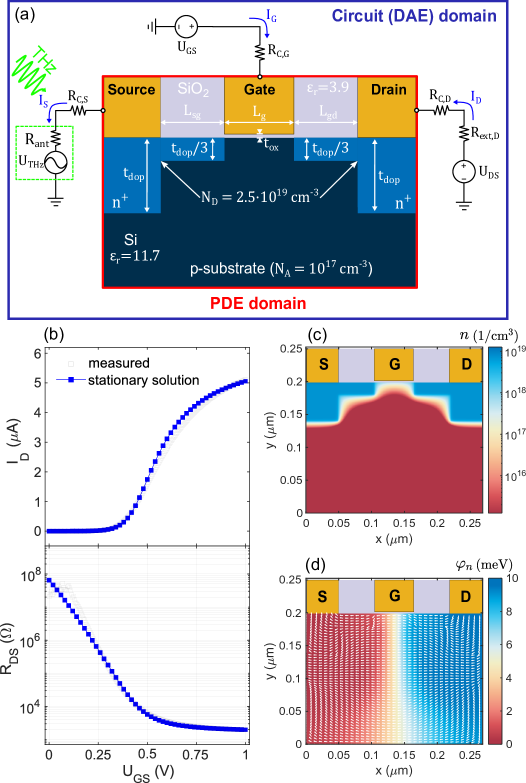
(b) Comparison of stationary (DC) TeraCAD simulation results with experimental characterization data for a 65-nm Si CMOS TeraFET for mV. Shown are the current at the drain terminal (top panel) and the drain-to-source resistance (bottom panel) as a function of the gate voltage .
(c,d) 2D distributions of the stationary electron density and the electron quasi-Fermi potential for mV and V. In (d), the overlaid white arrows depict the local flow direction of the electron current.
| Parameter | Description | Value |
| channel width | 0.7 m | |
| gate length | 60 nm | |
| and | gate-to-contact metallization distance | 55 nm |
| gate-to-channel oxide thickness1 | 3 nm | |
| doping depth | 60 nm |
-
1
Here, represents the effective insulator thickness (), which is the sum of the physical insulator thickness () and a quantum correction of due to the quantum-confinement effect of electrons at the Si/SiO2 interface in nanoscale MOSFETs [64]. is taken from the information sheet of TSMC for the 65-nm CMOS foundry process.
Here, is the effective density of states in the conduction band, with being the Boltzmann constant, the carrier temperature of the electrons, and the density-of-states effective mass of electrons in Si (: mass of free electrons) [65]. As already mentioned, we assumed K (room-temperature). represents the effective conduction band-edge energy, where is the conduction band-edge for the pure material and the intrinsic Fermi level. Note that here, and were assumed to be constant throughout the semiconductor. For heterostructure systems, these quantities can vary in space and need to be interpolated onto the cell interfaces as in case of and .
Fig. 1(a) presents the schematic of the simulated device. The geometric parameters are given in Table 1. As the actual net doping concentration and profile () were not known (they represent undisclosed information of the TSMC foundry), we determined such that the simulated curve of the stationary model is in fair agreement with the measured one, as shown in Fig. 1(b). For all simulations carried out in this work we used an uniform grid with nm and nm spacing. For the stationary simulations, we assumed Dirichlet boundary conditions for , and at the semiconductor-metal interfaces (ideal ohmic contacts) [40], thereby fixing the electron density at the contacts (visualized in Fig. 1(c)). We treated the gate electrode (a poly-Si gate stack [66, 67]) as an equipotential surface with an effective work function of eV (as for a poly-Si/TiN/SiO2 stack [68, 69, 70]). In order to close the unbounded PDE domain (red box in Fig. 1(a)) and to limit the computational load, we introduced artificial boundary conditions of von-Neumann type [40] for at the PDE domain edges and for and at the semiconductor domain edges (including the internal semiconductor-insulator (Si/SiO2) interface).222The artificial boundary of was chosen such that an increase of the PDE domain size did not significantly change the simulated resistance curve anymore. The von-Neumann boundary conditions imply that outward-orientated fluxes are prohibited and the PDE domain remains self-contained. Fig. 1(d)) displays the spatial dependence of the simulated electron quasi-Fermi potential for mV. The local direction of the electron current is indicated by white arrows.
The PDE domain was coupled to an external driver circuit (blue box in Fig. 1(a)), similar to that used in [71, 42], which represents a differential algebraic equation (DAE) that can be derived from Kirchhoff’s current and voltage laws. For the DC simulations of the current-voltage curve shown in the top panel of Fig. 1(b)), we set mV and varied . For the THz simulations, we coupled the THz wave to the source electrode (as indicated by the green box in Fig. 1(a)). The currents (including the displacement currents) at the source, drain and gate electrodes were calculated using the Ramo-Shockley theorem [72, 73]. For all simulations (DC and THz), we assumed a constant and real-valued antenna impedance of , an external parasitic resistance (corresponding to the approximate residual resistance of a protection FET in the real device), and a contact resistivity , which results in a contact resistance of for the given geometric parameters (see Table 1).
3 Hydrodynamic transport model
For the transient hydrodynamic simulations of n-channel Si MOSFETs, we considered only the dynamic response of the electrons and fixed the hole density in time to its respective stationary solution obtained for each gate voltage. The 2D isothermal HDM for electrons is given in conservation form by
| (6) |
with
Here, and represent the electric fields, and and the current densities, with and being the velocity components in - and -direction, respectively. They were determined from the eigenvalues of the differential operators and . They are defined by
| (7) | ||||
where m/s is the thermal (sound) velocity. The and are to be determined by the differential operators calculated from the unknown quantities obtained in the previous time step. For the scattering terms and the electron momentum relaxation time was determined from the high-field electron mobility via , with the effective mass and are defined by the scattering mechanisms discussed in the previous section.
To solve the multi-dimensional PDE system, we used the dimensional splitting approach (or fractional-step method) [74] with additional source-term splitting [52], applied for each direction separately. The scattering terms (e.g. of the -split) in was accounted for through an implicit Euler method [43]. The drift terms (e.g. of the -split) were incorporated in the well-balanced flux treatment as discussed below.
We tested two well-balanced schemes for the plasma wave simulations: The f-wave path-integral method [75] and the HLLC method [51, 52, 53]. Both are of upwind type (Riemann-problem-based), where information of the wave propagation is used to construct the numerical fluxes [52]. The HLLC method was found to be numerical stable and positivity-preserving for when applying large external fields together with strong doping gradients.333The f-wave path integral method was found to be stable only for the subsonic case. We emphasize here that both applied methods should be suitable for large-signal simulations of plasma waves, and the observed instability of the f-wave path method implemented in TeraCAD could not be investigated in course of the presented work. In Fig. 2(a), the Riemann problem for the HLLC method is depicted considering two adjacent cells (L = Left cell, R = Right cell). A Riemann problem is a special initial value problem (IVP) that contains a single discontinuity in the state variables at the initial time (shown here as an example for the electron density as green dashed line in Fig. 2(b)) that is considered together with the hyperbolic PDE. The solution to the Riemann problem results in shock waves that travel with a characteristic velocity in ether positive () or negative () direction along with intermediate states that exists between them. For the HLLC method two intermediate states, and , of the unknown vector are considered. These states are separated by the so-called contact wave ().
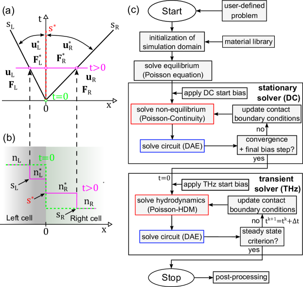
(c) A simplified flow chart for the TeraCAD simulations.
Before determining the HLLC fluxes and for the intermediate states, one seeks for a well-balanced condition of the isothermal HDM, that is, an exact equilibrium of carrier diffusion and carrier drift motion determined from the stationary solution (, ) of the HDM. For the -split, we have
| (8) |
where represents the thermal voltage. Integrating between the adjacent cells centered at positions and , one obtains
| (9) |
where and , and , accordingly. Eqn. (9) represents our well-balance condition between two adjacent cells. Taking Eqn. (9) into account and assuming a contact wave with speed between the intermediate states, we can determine the intermediate carrier densities and (as shown in Fig. 2(b)) from
| (10) | ||||
and the intermediate current density () from
| (11) | ||||
and represent the wave velocities in the left and right cell (see Fig. 2(a) and (b)), which are calculated from the characteristic speeds (Eqn. (7)) (-split) or (-split). The unknown HLL vector components and are given by [76, 77, 52]
| (12) | ||||
Note for our well-balanced scheme, the source term component due to the electric field () is directly included in the calculation of the intermediate current density (see Eq. 11). To ensure well-balancedness in thermal equilibrium, we need to calculated in the source term component by the so-called Roe average [52]. For the isothermal HDM with the well-balance property of Eqn. (9), we obtain
| (13) |
Finally, the HLLC fluxes can be obtained [52] from
| (14) | ||||
which are used to update the unknown vector through a conservative update. For the -split [52, 53]:
| (15) | ||||
For the -split, the update is performed in an analogous way. Note that, for numerical stability, the time step , where is the index of iteration, has to be estimated from the Courant-Friedrichs-Lewy (CFL) condition [52]
| (16) | ||||
where is the CFL coefficient, which is set to .
4 Simulation of the detector responsivity
Using the model described above, we simulated the detector response of a 65-nm Si CMOS TeraFET. In Fig. 2(c), the flow chart of the TeraCAD calculations is presented. After initialization of the simulation domain, the stationary solver was applied for different gate voltages . Since TeraFETs are in most cases operated without drain-to-source bias, V, they are by definition always in equilibrium before THz excitation. In Fig. 3(a), the resulting stationary carrier density in the channel of the MOSFET is plotted for V and V. Then, in the transient (HDM) solver, a sinusoidal excitation was applied to the source electrode (see Fig. 1(a)), where is the frequency and the amplitude of the THz voltage. The external excitation leads to a change in (as a consequence of the different boundary conditions at the contacts) which was calculated from the dynamic Poisson equation [42]
| (17) |
where is the dynamic electron density and the dynamic potential . (as shown in Fig. 3(a)) and correspond to stationary solutions of the PDEs. The PDE system was solved in sequence with the outer circuitry (see Fig. 1(a)), which represents a stiff differential algebraic equation (DAE) system of the form
| (18) |
derived from Kirchhoff’s laws and solved by an appropriate ODE solver. Note that the “mass” matrix contains all capacitance coefficients of the different metal electrodes, which are needed for the calculation of the displacement currents. The capacitances were determined from the Laplace equation (Eqn. (1) for zero space charge) [73].
The periodic change of leads to the development of plasma waves in the gated channel. To visualize these plasma waves, we plot in Fig. 3(b) the evolution of (top panel) and (bottom panel) with respect to their spatially dependent equilibrium values at different time steps (in units of ). The simulations were performed for THz. One observes an overdamped plasma wave, which is expected, as the value of was found to be 60 fs in the gated channel region and 12 fs in the highly doped contact regions, leading into .
Next, we determined the intrinsic detector efficiency, expressed in terms of the current responsivity , which can be obtained [71, 42] from
| (19) |
where is the rectified (DC) current arising from the plasma-wave-assisted distributed resistive mixing [6, 78] and is the THz (AC) power, which is coupled from the source electrode into the FET. These quantities were obtained as
| (20) | ||||
| (21) |
where and are the drain and source currents, respectively, and is the voltage at the source terminal. Note that the time dependence of the quantities arises for solutions, which have not yet reached the steady state. As steady-state criterion, we used in our simulations the relative deviation and demanded that .
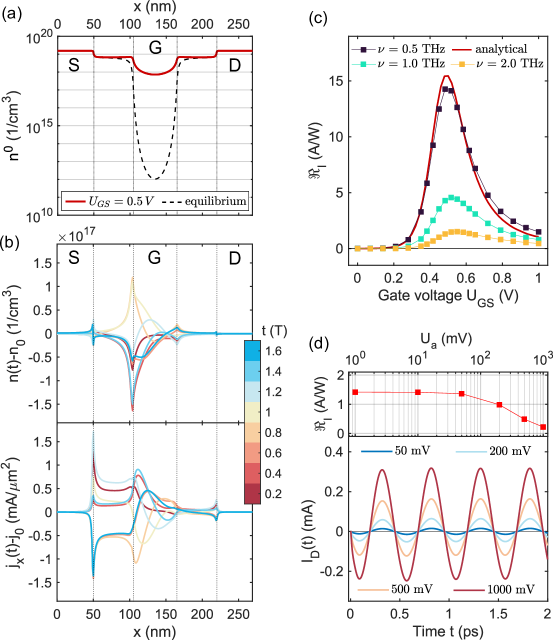
(b) Transient solver. Top panel: Oscillation of the carrier density with regards to equilibrium as a function of time (in units of , colorcoded). Bottom panel: Oscillation of the current density in x direction with regards to equilibrium . For both panels THz, V and mV.
(c) Gate voltage dependent current responsivity for different frequencies under small signal conditions (mV). The analytical approximation for resistive-self mixing detector response at THz (calculated with Eq. 22) is depicted as a red line.
(d) Time-dependent Drain terminal current as a function different THz amplitudes for a sinusoidal excitation at THz and V. The top inset depicts the steady-state current responsivity as a function of .
In Fig. 3(c), the simulated current responsivity is presented as function of the gate voltage for , 1 and 2 THz. In order to verify that our 2D HDM simulations yield correct values of the responsivity, we compare it with the expected low-frequency response of the detector calculated by
| (22) |
With this equation – derived in [79] by a small-signal analysis of the reduced transport equations, which account only for the drift motion of the charge carriers, i.e., consider only the resistive self-mixing regime at low THz frequencies, before plasma waves play a role –, the rectified current can be obtained from the simulated electrostatic transport properties of the MOSFET shown in Fig. 1(b). We find that the -curve obtained by our 2D hydrodynamic simulations at low frequency (0.5 THz) is in quantitative agreement with the current responsivity , calculated with Eq. (22) (see Fig. 3(c)). This represent a robust validation of our model and its numerical implementation for CMOS at low frequency and for small signals, i.e., for conditions, for which Eq. (22) has proven abundantly in the literature to yield good agreement with experimental results. With regard to the frequency dependence of , the strong decrease of the responsivity, which one observes in Fig. 3(c) is consistent with simulations performed for a simplified double-gate MOSFET in [42]. In the experiments of [33], a weaker frequency dependence was found, which may be attributed to the frequency dependence of the antenna impedance, which was neglected in the present work.
Finally, we present in Fig. 3(d)) results of large-signal HDM simulations to showcase the stability of our numerical method. The time dependence of the drain current is presented in the lower panel of Fig. 3(d)) for different THz amplitudes . We find that the well-balanced HLLC approximate Riemann solver is numerically stable even in case of enormous source terms (mV). The upper panel of Fig. 3(d) depicts the steady-state current responsivity as a function of . At larger THz amplitudes, the rectified current saturates. This is a consequence of carrier velocity saturation in the high-field regime, which is accounted for by the Caughey-Thomas mobility model [56].
5 Conclusion
To summarize, we have successfully implemented and applied a numerical method for 2D hyperbolic partial differential equations with strong source terms - the well-balanced HLLC approximate Riemann solver. It is well suited for the hydrodynamic modeling of electronic components in the THz frequency range. We tested the solver by simulating the THz response of a 65-nm Si CMOS TeraFET detector. The well-balanced HLLC approximate Riemann solver is found to be numerically stable and positivity-preserving for the carrier density even in the presence of strong doping gradients and large external THz excitations. With the use of the 2D Poisson equation for the calculation of the DC and THz electric fields, the solver copes with situations beyond the gradual channel approximation valid for the ultra-high frequency simulations. Our work extends recent advances in the field of plasma wave simulations in III-V compound semiconductors [44, 45] or graphene [46] devices. It is expected that the implementation method presented here for the isothermal case and for bulk semiconductors can be readily extended to the full hydrodynamic transport equations (including carrier heating) for the simulation of highly nonlinear carrier transport phenomena in semiconductor devices arising in the THz frequency regime upon large-signal excitation.
Acknowledgment
This work was funded by DFG RO 770/40-1, 770/40-2. We thank Prof. Dr.–Ing. C. Jungemann from the RWTH Aachen University for supplying us with his very helpful lecture notes on Numerical Device Simulation.
References
- [1] M. Dyakonov and M. Shur, “Shallow water analogy for a ballistic field effect transistor: New mechanism of plasma wave generation by dc current,” Physical Review Letters, vol. 71, no. 15, pp. 2465–2468, oct 1993. [Online]. Available: http://link.aps.org/doi/10.1103/PhysRevLett.71.2465
- [2] F. Crowne, “Contact boundary conditions and the Dyakonov–Shur instability in high electron mobility transistors,” Applied Physics Letters, vol. 82, p. 1242–1254, 1997.
- [3] C. Mendl and A. Lucas, “Dyakonov-Shur instability across the ballistic-to-hydrodynamic crossover,” Applied Physics Letters, vol. 112, p. 124101, 2020.
- [4] Z. Kargar, T. Linn, and C. Jungemann, “Investigation of the dyakonov–shur instability for thz wave generation based on the boltzmann transport equation,” Semicond. Sci. Technol., vol. 33, p. 104001, 2018.
- [5] M. Dyakonov and M. Shur, “Detection, mixing, and frequency multiplication of terahertz radiation by two-dimensional electronic fluid,” IEEE Transactions on Electron Devices, vol. 43, no. 3, pp. 380––387, 1996.
- [6] S. Boppel, A. Lisauskas, M. Mundt, D. Seliuta, L. Minkevicius, I. Kasalynas, G. Valusis, M. Mittendorff, S. Winnerl, V. Krozer, and H. G. Roskos, “CMOS integrated antenna-coupled field-effect transistors for the detection of radiation from 0.2 to 4.3 THz,” IEEE Transactions on Microwave Theory and Techniques, vol. 60, no. 12, pp. 3834–3843, 2012.
- [7] C. Jungemann, M. Noei, and T. Linn, “Device simulation of the Dyakonov-Shur plasma instability for THz wave generation,” in Proc. IEEE Latin American Electron Devices Conference (LAEDC), 2022.
- [8] W. Knap, J. Lusakowski, T. Parenty, S. Bollaert, A. Cappy, V. V. Popov, and M. S. Shur, “Terahertz emission by plasma waves in 60 nm gate high electron mobility transistors,” Applied Physics Letters, vol. 84, no. 13, pp. 2331–2333, mar 2004.
- [9] A. Lisauskas, U. Pfeiffer, E. Öjefors, P. H. Bolívar, D. Glaab, and H. G. Roskos, “Rational design of high-responsivity detectors of terahertz radiation based on distributed self-mixing in silicon field-effect transistors,” Journal of Applied Physics, vol. 105, no. 11, p. 114511, 2009. [Online]. Available: https://dx.doi.org/10.1063/1.3140611
- [10] A. Lisauskas, S. Boppel, M. Mundt, V. Krozer, and H. G. Roskos, “Subharmonic mixing with field-effect transistors: Theory and experiment at 639 GHz high above ft,” IEEE SENSORS JOURNAL, vol. 13, no. 1, p. 9, 2013.
- [11] D. Glaab, S. Boppel, A. Lisauskas, U. Pfeiffer, E. Öjefors, and H. G. Roskos, “Terahertz heterodyne detection with silicon field-effect transistors,” Applied Physics Letters, vol. 96, no. 4, p. 042106, jan 2010. [Online]. Available: http://aip.scitation.org/doi/10.1063/1.3292016
- [12] S. Boppel, A. Lisauskas, A. Max, V. Krozer, and H. G. Roskos, “CMOS detector arrays in a virtual 10-kilopixel camera for coherent terahertz real-time imaging,” Optics Letters, vol. 37, no. 4, pp. 536–538, FEB 15 2012.
- [13] G. Valušis, A. Lisauskas, H. Yuan, W. Knap, and H. G. Roskos, “Roadmap of terahertz imaging 2021,” Sensors, vol. 21, p. 4092, 2021.
- [14] H. Yuan, A. Lisauskas, M. D. Thomson, and H. G. Roskos, “600-GHz Fourier imaging based on heterodyne detection at the 2nd sub-harmonic,” Optics Express, vol. 31, no. 24, pp. 40 856–40 870, 2023.
- [15] M. M. Wiecha, R. Kapoor, A. V. Chernyadiev, K. Ikamas, A. Lisauskas, and H. G. Roskos, “Antenna-coupled field-effect transistors as detectors for terahertz near-field microscopy,” Nanoscale Advances, vol. 3, no. 6, pp. 1717–1724, 2021. [Online]. Available: http://xlink.rsc.org/?DOI=D0NA00928H
- [16] P. Hillger, J. Grzyb, R. Jain, and U. R. Pfeiffer, “Terahertz imaging and sensing applications with silicon-based technologies,” IEEE Transactions on Terahertz Science and Technology, vol. 9, no. 1, pp. 1–19, Jan. 2019.
- [17] K. Ikamas, D. Cibiraite, A. Lisauskas, M. Bauer, V. Krozer, and H. G. Roskos, “Broadband terahertz power detectors based on 90-nm silicon CMOS transistors with flat responsivity up to 2.2 THz,” IEEE Electron Device Letters, vol. 39, no. 9, pp. 1413–1416, sep 2018.
- [18] H. W. Hou, Z. Liu, J. H. Teng, T. Palacios, and S. J. Chua, “High temperature terahertz detectors realized by a GaN high electron mobility transistor,” Scientifc Reports, vol. 7, p. 46664, 2017.
- [19] S. Regensburger, A. K. Mukherjee, S. Schönhuber, M. A. Kainz, S. Winnerl, J. M. Klopf, H. Lu, A. C. Gossard, K. Unterrainer, and S. Preu, “Broadband terahertz detection with zero-bias field-effect transistors between 100 GHz and 11.8 THz with a noise equivalent power of 250 pW/ at 0.6 THz,” IEEE Transactions on Terahertz Science and Technology, vol. 8, no. 4, pp. 465–471, 2018.
- [20] M. Bauer, A. Rämer, S. A. Chevtchenko, K. Y. Osipov, D. Čibiraitė, S. Pralgauskaitė, K. Ikamas, A. Lisauskas, W. Heinrich, V. Krozer, and H. G. Roskos, “A high-sensitivity AlGaN/GaN HEMT terahertz detector with integrated broadband bow-tie antenna,” IEEE Transactions on Terahertz Science and Technology, vol. 9, no. 4, pp. 430–444, 2019.
- [21] S. Regensburger, F. Ludwig, S. Winnerl, J. M. Klopf, H. Lu, H. G. Roskos, and S. Preu, “Mapping the slow and fast photoresponse of field-effect transistors to terahertz and infrared radiation,” Optics Express, vol. 32, no. 5, p. 8458, 2024.
- [22] A. Zak, M. A. Andersson, M. Bauer, J. Matukas, A. Lisauskas, H. G. Roskos, and J. Stake, “Antenna-integrated 0.6 THz FET direct detectors based on CVD graphene,” Nano Letters, vol. 14, no. 10, pp. 5834–5838, 2014.
- [23] A. A. Generalov, M. A. Andersson, X. Yang, A. Vorobiev, and J. Stake, “A heterodyne graphene FET detector at 400 GHz,” in 2017 42nd International Conference on Infrared, Millimeter, and Terahertz Waves (IRMMW-THz), 2017, pp. 1–2.
- [24] L. Viti, D. G. Purdie, A. Lombardo, A. C. Ferrari, and M. S. Vitiello, “HBN-encapsulated, graphene-based, room-temperature terahertz receivers, with high speed and low noise,” Nano Letters, vol. 20, p. 3169–77, 2020.
- [25] F. Ludwig, A. Generalov, J. Holstein, M. A., K. Viisanen, M. Prunilla, and H. G. Roskos, “Terahertz detection with graphene FETs: Photothermoelectric and resistive self-mixing contributions to the detector response,” ACS Applied Electronic Materials, vol. 6, pp. 2197–2212, 2024.
- [26] L. Viti, A. R. Cadore, X. Yang, A. Vorobiev, J. E. Muench, K. Watanabe, T. Taniguchi, J. Stake, A. C. Ferrari, and M. S. Vitiello, “Thermoelectric graphene photodetectors with sub-nanosecond response times at terahertz frequencies,” Nanophotonics, vol. 10, no. 1, pp. 89–98, 2021.
- [27] P. Martín-Mateos, D. Čibiraitė Lukenskienė, R. Barreiro, C. de Dios, A. Lisauskas, V. Krozer, and P. Acedo, “Hyperspectral terahertz imaging with electro-optic dual combs and a FET-based detector,” Scientific Reports, vol. 10, p. 14429, 2020.
- [28] C. Drexler, N. Dyakonova, P. Olbrich, J. Karch, M. Schafberger, K. Karpierz, Y. Mityagin, M. B. Lifshits, F. Teppe, O. Klimenko, Y. M. Meziani, W. Knap, and S. D. Ganichev, “Helicity sensitive terahertz radiation detection by field effect transistors,” Journal of Applied Physics, vol. 111, no. 12, p. 124504, 2012.
- [29] D. A. Bandurin, D. Svintsov, I. Gayduchenko, S. G. Xu, A. Principi, M. Moskotin, I. Tretyakov, and et al., “Resonant terahertz detection using graphene plasmons,” Nature Communications, vol. 9, p. 5392, 2018.
- [30] J. M. Caridad, O. Castelló, S. M. L. Baptista, T. Taniguchi, K. Watanabe, H. G. Roskos, and J. A. Delgado-Notario, “Room-temperature plasmon-assisted resonant THz detection in single-layer graphene transistors,” Nano Letters, vol. 24, p. 935–942, 2024.
- [31] A. Soltani, F. Kuschewski, M. Bonmann, A. Generalov, A. Vorobiev, F. Ludwig, M. M. Wiecha, D. Čibiraitė, F. Walla, S. Winnerl, S. C. Kehr, L. M. Eng, J. Stake, and H. G. Roskos, “Direct nanoscopic observation of plasma waves in the channel of a graphene field-effect transistor,” Light: Science and Applications, vol. 9, p. 97, 2020.
- [32] F. Ludwig, M. Bauer, A. Lisauskas, and H. G. Roskos, “Circuit-based hydrodynamic modeling of AlGaN/GaN HEMTs,” in ESSDERC 2019 - 49th European Solid-State Device Research Conference (ESSDERC), 2019, pp. 270–273.
- [33] F. Ludwig, J. Holstein, A. Krysl, A. Lisauskas, and H. G. Roskos, “Modeling of antenna-coupled Si MOSFETs in the terahertz frequency range,” IEEE Transactions on Terahertz Science and Technology, vol. 14, no. 3, pp. 1–11, 2024.
- [34] M. A. Andersson and J. Stake, “An accurate empirical model based on Volterra series for FET power detectors,” IEEE Transactions on Microwave Theory and Techniques, vol. 64, no. 5, pp. 1431–1441, may 2016.
- [35] K. Bløtekjær, “Transport equations for electrons in two-valley semiconductors,” IEEE Transactions on Electron Devices, vol. 17, p. 38–47, 1970.
- [36] T. Grasser, T.-W. Tang, H. Kosina, and S. Selberherr, “A review of hydrodynamic and energy-transport models for semiconductor device simulation,” Proceedings of the IEEE, vol. 91, no. 2, pp. 251–274, 2003.
- [37] A. Gutin, V. Kachorovskoii, and A. M. M. Shur, “Plasmonic terahertz detector response to high intensities,” Journal of Applied Physics, vol. 112, p. 014508, 2012.
- [38] S. Rudin, G. Rupper, A. Gutin, and M. Shur, “Theory and measurement of plasmonic terahertz detector response to large signals,” Journal of Applied Physics, vol. 115, p. 064503, 2014.
- [39] D. Scharfetter and H. Gummel, “Large-signal analysis of a silicon read diode oscillator,” IEEE Transactions on Electron Devices, vol. 16, no. 1, pp. 64–77, 1969.
- [40] S. Selberherr, Analysis and Simulation of Semiconductor Devices, 1st ed. Springer Vienna, 1984.
- [41] X. Liu and M. Shur, “An efficient TCAD model for TeraFET detectors,” IEEE Radio and Wireless Symposium, p. 1–4, 2019.
- [42] T. Linn, K. Bittner, Brachtendorf, H.G., and C. Jungemann, “Simulation of THz oscillations in semiconductor devices based on balance equations,” J Sci Comput, vol. 85, p. 6, 2020.
- [43] R. J. LeVeque, Finite Difference Methods for Ordinary and Partial Differential Equations: Steady-State and Time-Dependent Problems. Society for Industrial and Applied Mathematics, Jan. 2007. [Online]. Available: http://epubs.siam.org/doi/book/10.1137/1.9780898717839
- [44] S. Bhardwaj, F. L. Teixeira, and J. L. Volakis, “Fast modeling of terahertz plasma-wave devices using unconditionally stable fdtd methods,” IEEE Journal on Multiscale and Multiphysics Computational Techniques, vol. 3, pp. 29–36, 2018.
- [45] S. Bhardwaj, “Electronic–electromagnetic multiphysics modeling for terahertz plasmonics: A review,” IEEE Journal on Multiscale and Multiphysics Computational Techniques, vol. 4, pp. 307–316, 2019.
- [46] P. Cosme, J. S. Santos, J. P. S. Bizarro, and I. Figueiredo, “TETHYS: A simulation tool for graphene hydrodynamic models,” Computer Physics Communications, vol. 282, p. 108550, 2023.
- [47] A. Kurganov and G. Petrova, “A second-order well-balanced positivity preserving central-upwind scheme for the Saint-Venant system,” Communications in Mathematical Sciences, vol. 5, no. 1, pp. 133–160, 2007.
- [48] A. Kurganov, “Finite-volume schemes for shallow-water equations,” Acta Numerica, vol. 27, pp. 289–351, May 2018.
- [49] I. Cravero, G. Puppo, M. Semplice, and G. Visconti, “Cool WENO schemes,” Computers & Fluids, vol. 169, pp. 71–86, 2018.
- [50] I. Cravero, M. Semplice, and G. Visconti, “Optimal definition of the nonlinear weights in multidimensional central WENOZ reconstructions,” SIAM Journal on Numerical Analysis, vol. 57, no. 5, pp. 2328–2358, 2019.
- [51] E. F. Toro, M. Spruce, and W. Speares, “Restoration of the contact surface in the HLL-Riemann solver,” Shock Waves, vol. 4, no. 1, pp. 25–34, Jul. 1994. [Online]. Available: http://link.springer.com/10.1007/BF01414629
- [52] E. F. Toro, Riemann solvers and numerical methods for fluid dynamics: a practical introduction, 3rd ed. USA: Dordrecht New York: Springer, 2009.
- [53] E. Audusse, C. Chalons, and P. Ung, “A simple well-balanced and positive numerical scheme for the shallow-water system,” Communications in Mathematical Sciences, vol. 13, no. 5, pp. 1317–1332, 2015. [Online]. Available: http://www.intlpress.com/site/pub/pages/journals/items/cms/content/vols/0013/0005/a011/
- [54] D. Cole and J. Johnson, “Accounting for incomplete ionization in modeling silicon based semiconductor devices,” in Proceedings of the Workshop on Low Temperature Semiconductor Electronics,, 1989, pp. 73–77.
- [55] J. Piprek, Handbook of Optoelectronic Device Modeling and Simulation, 1st ed. CRC Press Taylor and Francis Group, 2017, vol. 2, pp. 733–771.
- [56] D. Caughey and R. Thomas, “Carrier mobilities in silicon empirically related to doping and field,” Proceedings of the IEEE, vol. 55, no. 12, pp. 2192–2193, 1967.
- [57] W. Van Roosbroeck, “Theory of the Flow of Electrons and Holes in Germanium and Other Semiconductors,” Bell System Technical Journal, vol. 29, no. 4, pp. 560–607, Oct. 1950. [Online]. Available: https://ieeexplore.ieee.org/document/6772705
- [58] C. Lombardi, S. Manzini, A. Saporito, and M. Vanzi, “A physically based mobility model for numerical simulation of nonplanar devices,” IEEE Transactions on Computer-Aided Design of Integrated Circuits and Systems, vol. 7, no. 11, pp. 1164–1171, 1988.
- [59] G. Masetti, M. Severi, and S. Solmi, “Modeling of carrier mobility against carrier concentration in arsenic-, phosphorus-, and boron-doped silicon,” IEEE Transactions on Electron Devices, vol. 30, no. 7, pp. 764–769, 1983.
- [60] W. Shockley and W. T. Read, “Statistics of the recombinations of holes and electrons,” Phys. Rev., vol. 87, pp. 835–842, Sep 1952. [Online]. Available: https://link.aps.org/doi/10.1103/PhysRev.87.835
- [61] M. A. der Maur, “A multiscale simulation environment for electronic and optoelectronic devices,” dissertation, Università degli Studi di Roma – Tor Vergata, 2008. [Online]. Available: http://www.optolab.uniroma2.it/images/stories/team/aufdermaur/thesis_aufdermaur.pdf
- [62] D. Vasileska, S. M. Goodnick, and G. Klimeck, Computational Electronics: Semiclassical and Quantum Device Modeling and Simulation, 1st ed. CRC Press. [Online]. Available: https://www.taylorfrancis.com/books/9781420064841
- [63] W. H. Press, S. A. Teukolsky, W. T. Vetterling, and B. P. Flannery, Numerical Recipes 3rd Edition: The Art of Scientific Computing, 3rd ed. USA: Cambridge University Press, 2007.
- [64] I. Saad, M. L. P. Tan, M. T. Ahmadi, R. Ismail, and V. K. Arora, “The dependence of saturation velocity on temperature, inversion charge and electric field in a nanoscale MOSFET,” International Journal of Nanoelectronics and Materials, vol. 3, pp. 17–34, 2010.
- [65] M. A. Green, “Intrinsic concentration, effective densities of states, and effective mass in silicon,” Journal of Applied Physics, vol. 67, no. 6, pp. 2944–2954, Mar. 1990.
- [66] S. Fung, H. Huang, S. Cheng, K. Cheng, S. Wang, Y. Wang, Y. Yao, C. Chu, S. Yang, W. Liang, Y. Leung, C. Wu, C. Lin, S. Chang, S. Wu, C. Nieh, C. Chen, T. Lee, Y. Jin, S. Chen, L. Lin, Y. Chiu, H. Tao, C. Fu, S. Jang, K. Yu, C. Wang, T. Ong, Y. See, C. Diaz, M. Liang, and Y. Sun, “65nm CMOS high speed, general purpose and low power transistor technology for high volume foundry application,” in Digest of Technical Papers. 2004 Symposium on VLSI Technology, 2004., 2004, pp. 92–93.
- [67] S. Yang, J. Sheu, M. Ieong, M. Chiang, T. Yamamoto, J. Liaw, S. Chang, Y. Lin, T. Hsu, J. Hwang, J. Ting, C. Wu, K. Ting, F. Yang, C. Liu, I. Wu, Y. Chen, S. Chent, K. Chen, J. Cheng, M. Tsai, W. Chang, R. Chen, C. Chen, T. Lee, C. Lin, S. Yang, Y. Sheu, J. Tzeng, L. Lu, S. Jang, C. Diaz, and Y. Mii, “28nm metal-gate high-K CMOS SoC technology for high-performance mobile applications,” in 2011 IEEE Custom Integrated Circuits Conference (CICC). San Jose, CA, USA: IEEE, Sep. 2011, pp. 1–5. [Online]. Available: http://ieeexplore.ieee.org/document/6055355/
- [68] R. Singanamalla, H. Y. Yu, B. Van Daele, S. Kubicek, and K. De Meyer, “Effective Work-Function Modulation by Aluminum-Ion Implantation for Metal-Gate Technology $(\hbox{Poly-Si/TiN/SiO}_{2})$,” IEEE Electron Device Letters, vol. 28, no. 12, pp. 1089–1091, Dec. 2007. [Online]. Available: http://ieeexplore.ieee.org/document/4383548/
- [69] M. Kadoshima, T. Matsuki, S. Miyazaki, K. Shiraishi, T. Chikyo, K. Yamada, T. Aoyama, Y. Nara, and Y. Ohji, “Effective-Work-Function Control by Varying the TiN Thickness in Poly-Si/TiN Gate Electrodes for Scaled High- $k$ CMOSFETs,” IEEE Electron Device Letters, vol. 30, no. 5, pp. 466–468, May 2009. [Online]. Available: https://ieeexplore.ieee.org/document/4808212
- [70] J. Robertson, “Band offsets and work function control in field effect transistors,” Journal of Vacuum Science & Technology B: Microelectronics and Nanometer Structures Processing, Measurement, and Phenomena, vol. 27, no. 1, pp. 277–285, Jan. 2009. [Online]. Available: https://pubs.aip.org/jvb/article/27/1/277/1046345/Band-offsets-and-work-function-control-in-field
- [71] C. Jungemann, K. Bittner, and H. G. Brachtendorf, “Simulation of plasma resonances in mosfets for thz-signal detection,” Joint International EUROSOI Workshop and International Conference on Ultimate Integration on Silicon, p. 48–51, 2016.
- [72] S. Ramo, “Currents induced by electron motion,” Proceedings of the IRE, vol. 27, no. 9, pp. 584–585, 1939.
- [73] H. Kim, H. Min, T. Tang, and Y. Park, “An extended proof of the Ramo-Shockley theorem,” Solid-State Electronics, vol. 34, no. 11, pp. 1251–1253, Nov. 1991. [Online]. Available: https://linkinghub.elsevier.com/retrieve/pii/0038110191900657
- [74] N. N. Yanenko, The Method of Fractional Steps, M. Holt, Ed. Berlin, Heidelberg: Springer Berlin Heidelberg, 1971. [Online]. Available: http://link.springer.com/10.1007/978-3-642-65108-3
- [75] R. J. LeVeque, “A Well-Balanced Path-Integral f-Wave Method for Hyperbolic Problems with Source Terms,” Journal of Scientific Computing, vol. 48, no. 1-3, pp. 209–226, Jul. 2011. [Online]. Available: http://link.springer.com/10.1007/s10915-010-9411-0
- [76] A. Harten, P. D. Lax, and B. V. Leer, “On Upstream Differencing and Godunov-Type Schemes for Hyperbolic Conservation Laws,” SIAM Review, vol. 25, no. 1, pp. 35–61, Jan. 1983. [Online]. Available: http://epubs.siam.org/doi/10.1137/1025002
- [77] F. Bouchut, “An introduction to finite volume methods forhyperbolic conservation laws,” ESAIM: Proceedings, vol. 15, pp. 1–17, 2005. [Online]. Available: http://www.esaim-proc.org/10.1051/proc:2005020
- [78] E. Öjefors, U. R. Pfeiffer, A. Lisauskas, and H. G. Roskos, “A 0.65 THz focal-plane array in a quarter-micron CMOS process technology,” IEEE Journal of Solid-State Circuits, vol. 44, no. 7, pp. 1968–1976, 2009.
- [79] M. Sakowicz, M. B. Lifshits, O. A. Klimenko, F. Schuster, D. Coquillat, F. Teppe, and W. Knap, “Terahertz responsivity of field effect transistors versus their static channel conductivity and loading effects,” Journal of Applied Physics, vol. 110, no. 5, p. 054512, sep 2011. [Online]. Available: http://doi.org/10.1063/1.3632058