[1,2]\fnmPaul \surSzypryt
1]\orgdivDepartment of Physics, \orgnameUniversity of Colorado, \orgaddress\cityBoulder, \stateCO, \countryUSA
2]\orgnameNational Institute of Standards and Technology, \orgaddress\cityBoulder, \stateCO, \countryUSA
3]\orgdivDepartment of Physics, \orgnameUniversity of Milano Bicocca, \orgaddress\cityMilan, \countryItaly
a]Currently at \orgnameQuantum Design, Inc, \orgaddress\citySan Diego, \stateCA, \countryUSA
b]Currently at \orgnameAWS Center for Quantum Computing, \orgaddress\cityPasadena, \stateCA, \countryUSA
Kinetic inductance current sensor for visible to near-infrared wavelength transition-edge sensor readout
Abstract
Single-photon detectors based on the superconducting transition-edge sensor (TES) are used in a number of visible to near-infrared (VNIR) applications, particularly for photon-number-resolving measurements in quantum information science. To be practical for large-scale photonic quantum computing or for future spectroscopic imaging applications in astronomy, the size of VNIR TES arrays must be increased from a few pixels to many thousands. Historically, TES arrays have been read out with multiplexed superconducting quantum interference devices (SQUIDs), but the microsecond-duration pulse signals of VNIR TESs are notoriously difficult to multiplex. In this manuscript, we introduce the kinetic inductance current sensor (KICS), a more readily scalable readout technology that exploits the nonlinear kinetic inductance in a superconducting resonator to make sensitive current measurements. KICS devices can replace SQUIDs for many applications because of their ability to measure fast, high slew-rate signals, their compatibility with standard microwave frequency-division multiplexing techniques, and their relatively simple fabrication. Here, we demonstrate the readout of a VNIR TES using a KICS with \qty3.7MHz of bandwidth. We measure a readout noise of \qty1.4pA/Hz, considerably below the TES noise at frequencies of interest, and a TES energy resolution of \qty0.137 ±0.001eV at \qty0.8eV, comparable to resolutions observed with non-multiplexed SQUID readouts.
Introduction
The transition-edge sensor (TES) [1, 2] has long been used in bolometers [3] for sensitive power measurement and calorimeters [4, 5, 6] for energy-resolved single-photon detection. At visible to near-infrared (VNIR) wavelengths, the TES calorimeter has a number of advantages over more conventional detectors, such as broad wavelength coverage, intrinsic energy resolution, high quantum efficiency (QE), short (microsecond) photon detection timescales, and negligible dark counts [5, 7, 8]. These qualities have facilitated the experimental testing of fundamental laws of quantum mechanics, in the setting of loophole-free Bell tests [9, 10, 11], and photonic quantum computing [12, 8]. They also make the VNIR TES well-suited for exoplanet atmospheric spectroscopy [13, 14] and biological imaging [15, 16], among other applications. These measurements, however, are limited by the small array sizes currently achieved.
In a TES calorimeter, a superconducting thin film is cooled below its superconducting critical temperature, , and then electrically biased into the superconducting-to-normal transition. In this narrow region, the device resistance depends strongly on temperature, causing absorbed photons that increase the TES temperature to also measurably raise its resistance. Under voltage bias, the TES current response provides a sensitive measurement of an absorbed photon’s energy.
Much of the difficulty with TES operation comes in the readout of large arrays. Generally, TESs need to be multiplexed at the cryogenic stage to reduce wiring complexity, thermal loads, and power consumption. In multiplexed readout, signals from many individual TESs are encoded in an orthogonal basis set, measured through a shared cryogenic amplifier chain, and decoded at room temperature. TES currents have historically been read out with superconducting quantum interference devices (SQUIDs) [17] through a variety of multiplexing schemes [18]. The most mature of these is time-division multiplexing (TDM) [19, 20, 21], but MHz frequency-division multiplexing (FDM) [22, 23] and microwave SQUID multiplexing (MUX) [24, 25] systems have also been implemented. Kilopixel-scale readouts are now typical in long-wavelength bolometers [26, 27, 28] and are actively being developed for x-ray calorimeters [29, 30]. These readouts have been more challenging to realize for the faster VNIR TESs. In TDM, the sampling interval (typically microseconds) is limited by sequential switching of DC-SQUIDs [20, 21]. FDM readouts with MHz carrier frequencies are typically limited to 100-kHz-scale signal bandwidths [23]. In MUX, the flux ramp signal used to linearize the RF-SQUID response limits the sampling rate, and operating a sufficiently fast flux ramp without degrading performance has proved difficult [31, 32].
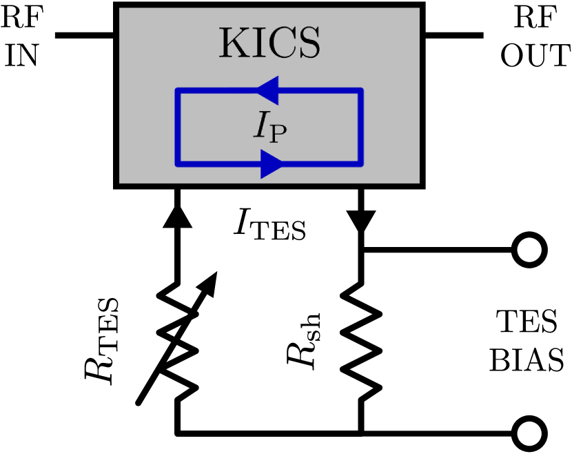
Here, we introduce the kinetic inductance current sensor (KICS), a superconducting resonator-based device that replaces the SQUID in the readout circuit of a TES or other cryogenic detector/device. The KICS, shown schematically in Fig. 1, exploits the nonlinear current dependence of the kinetic inductance in a superconductor. This nonlinearity has previously been explored in other superconducting devices such as the kinetic inductance traveling-wave parametric amplifier (KITWPA) [33, 34, 35] and the kinetic inductance parametric up-converter (KPUP) [36, 37]. The form of the kinetic inductance nonlinearity can be derived from Ginzburg-Landau theory [38] and expanded [39] as
| (1) |
Here, is the inductor current, and , which is on order the superconducting critical current , sets the magnitude of the nonlinearity and depends on the inductor material and cross-sectional area. As the resonant frequency, , goes as , it can be arbitrarily set by adjusting up to . We define the current sensitivity, or responsivity, as , where is the fractional frequency shift. To leading order, . The responsivity, therefore, can be increased by applying a bias current. Readout is done in much the same way as the microwave kinetic inductance detector (MKID) [40, 41, 39], another superconducting resonator-based device. Here, a microwave transmission line couples the device to room temperature readout electronics which monitor shifts in the resonant frequency.

Central to the KICS scheme is a superconducting switch, , that is used to trap a persistent current, , in the resonator through the requirement of flux quantization. This is analogous to the biasing scheme of metallic magnetic calorimeters (MMCs) [42] and provides several critical advantages over other microwave domain readouts such as MUX and KPUPs. First, the persistent current allows the KICS to be self-biased in the high responsivity regime. This prevents pickup in the bias line from entering the KICS circuit and reduces noise when compared to an actively biased device. Additionally, this self-biasing method is dissipationless, reducing power consumption. Finally, superconducting resonator-based detectors and readouts have historically been plagued by fabrication imperfections that cause resonances to deviate from their designed values, creating frequency collisions that reduce device yield [24, 43]. The KICS biasing scheme overcomes this issue through continuous frequency tunability [44] and superconducting switches that lock resonances at desired points.
The KICS has further advantages over SQUID readouts. As discussed above, fast detector timescales, such as those observed in VNIR TESs, can make SQUID-based multiplexing difficult. The KICS readout speed, however, is effectively set by the designed resonator bandwidth and can be matched to these fast devices. Furthermore, large and dense arrays are essential for most imaging applications, likely requiring integrated detector and readout fabrication, but SQUIDs have not yet been adapted for this format. For one, fabrication of SQUID readouts can be complex, requiring small and highly uniform junctions and many fabrication steps and materials [45, 24]. KICS devices require only a single layer for the critical resonator structures, making high-yield integrated fabrication more feasible. Additionally, KICSs have the potential to be significantly smaller than SQUIDs and thus can be more easily integrated within a TES array. Current is coupled galvanically to a KICS rather than inductively as in a SQUID. As a result, a KICS does not require large coupling coils and associated features that mitigate cross-talk and unwanted backgrounds [46]. SQUID readout cells are typically \qty¿0.4mm\squared [8, 47, 46]), whereas the KICS follows many of the design principles of MKIDs for which much more compact designs (\qty0.02mm\squared) have already been demonstrated [43].
The KICS can be used to sensitively measure the current from a variety of superconducting devices historically read out with SQUIDs. This includes TES-based detectors operating across the electromagnetic spectrum as well as MMCs. In this manuscript, we demonstrate the KICS concept through the readout of a VNIR TES, which, as noted above, has been especially challenging to multiplex and read out with SQUIDs.
Results
Device and setup
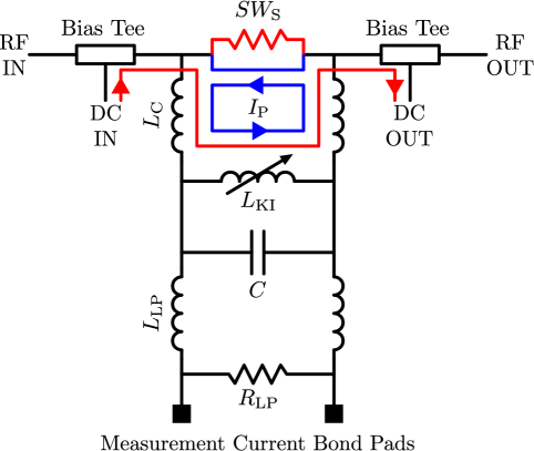
The KICS used in this study is adapted from a previous tunable resonator design [44]. The fabrication involves only a single \qty20nm thick NbTiN layer with and sheet inductance . This layer was patterned to form the resonator, microstrip transmission line, and coupling and filter inductors. To increase the degree of nonlinearity, the width of the resonator inductor was designed to be small (\qty0.7μm). In this initial implementation, Al wire bonds () were placed over a gap in the transmission line to form a thermally-activated superconducting switch. A filter resistor, , consisting of a thin layer of Au on Si was wire bonded into the circuit. The dominant inductance in the readout circuit is , as is on order \qty1nH.
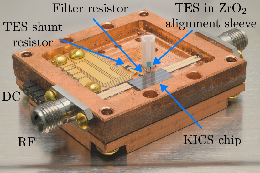
The VNIR TES is a \qty20μm square trilayer consisting of \qty2nm amorphous Si (a-Si), \qty20nm W, and \qty2nm a-Si, similar to previously reported devices [7, 8]. The a-Si is used to stabilize [48], here \qty188mK. The TES chip was micromachined to match the inner diameter of a zirconia (ZrO2) sleeve, allowing self-alignment of the TES to an optical fiber [49]. To voltage-bias the TES, a commercially available \qty10mΩ shunt resistor, , was connected via wire bonds. The full KICS and TES assembly is shown in Fig. 2.
An adiabatic demagnetization refrigerator (ADR) with base temperature \qty¡40mK was used to cool the device. The cryostat was outfitted with the necessary DC and RF cabling, high-electron mobility transistor (HEMT) amplifiers, and single-mode (SM) fiber to fully interface with the device. Characterization was done using a vector network analyzer (VNA) and microwave homodyne readout, common in MKID measurements [41]. Additional experimental setup details can be found in Methods.
Responsivity and noise
To begin characterization of the KICS, the ADR temperature was set to \qty1.6K, well below the of the NbTiN resonator but above the of the Al superconducting switch. Here, a DC current, , applied at the bias tee is forced to travel around the switch and through the resonator. The VNA was used to measure the KICS complex transmission as a function of .
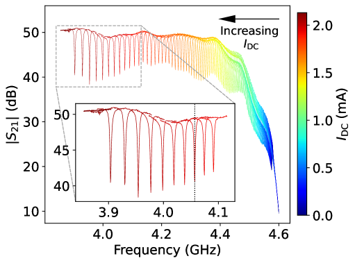
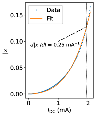
As shown in the left panel of Fig. 3, as was swept upwards, decreases due to increasing . For this broad sweep, was calculated at the local minimum of the transmission magnitude. The resonant frequency was measured to be at and had a maximal frequency shift of \qty∼700MHz at , as determined by the sudden decline of the resonator . The fractional frequency shift, , is plotted against in the right panel of Fig. 3. These data were fit to the form of Eqn. 1 to extract and .
To prepare the VNIR TES readout, was set to \qty1.95mA, where . This bias point was selected to maximize while still being far enough from to prevent current fluctuations from driving the inductor normal and releasing . With the bias set, the ADR temperature was lowered below the of the Al superconducting switch, trapping the bias current in the resonator and establishing . At this bias point, , a shift of nearly \qty520MHz. The zero point of was moved to this frequency for subsequent measurements, hereafter . The resonator bandwidth was measured to be \qty3.7MHz (, largely coupling-limited), sufficient for tracking current changes in the TES with expected microsecond timescales.
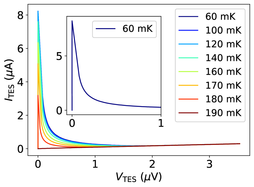
After locking in the KICS bias, TES IV curves were collected at temperatures between \qty60mK and \qty190mK, as shown in Fig. 4. At each temperature, the TES bias was stepped from high to low, shifting the TES current, , and in turn the KICS . The measured was used to convert to . An operating temperature of \qty60mK was chosen to perform the remainder of TES measurements, although we note that the TES performance (and IV curve) was largely insensitive to operating temperature this far below the TES . The IV curve at \qty60mK was used to select a TES bias point of , where is the TES normal state resistance. Although this bias point is lower than what is typically used with SQUID readouts, here we found it to result in optimal photon energy resolution without causing TES instability.
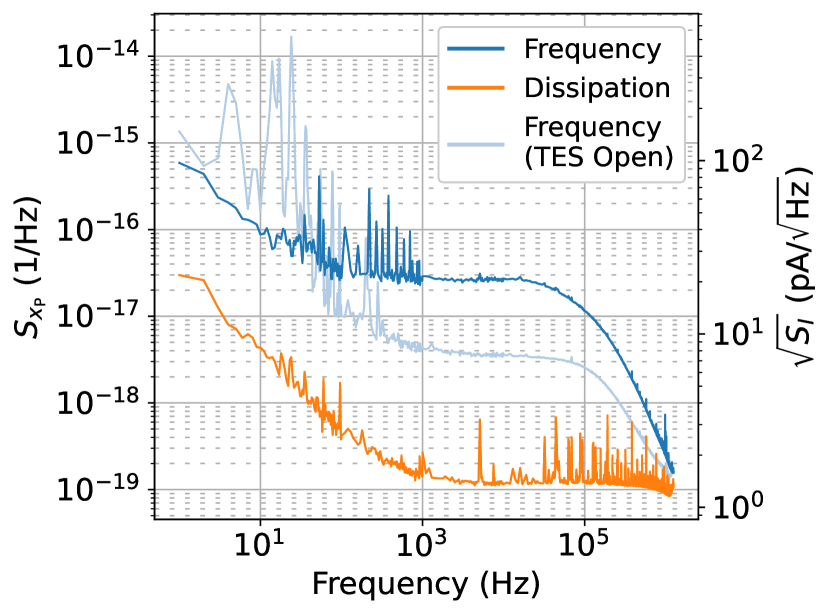
Noise data were collected with a microwave homodyne readout setup. The probe tone was set to the KICS resonance with a power of \qty-70dBm at the input of the device box, driving the resonator to the onset of bifurcation. Traces in the readout’s IQ (in-phase and quadrature) mixer outputs were collected for a total of \qty30s. Using a frequency sweep of the resonator transmission, these traces were projected onto the frequency and dissipation quadratures (tangent and orthogonal to the resonance circle in the complex plane) and converted to fractional frequency shift units, . Fourier transform techniques were then used to calculate the noise power spectral density (PSD), , as shown in Fig. 5. The frequency-quadrature noise is particularly important as this quadrature is most sensitive to the largely dissipationless KICS current response. We note that for the fast TES timescales, only the noise at high frequencies ( kHz) is significant for detector performance. The measured was used to calculate the current noise, , and predict a mean TES white noise level of \qty21pA/Hz between \qty2kHz and \qty20kHz. This includes the contribution from the filter Johnson noise (\qty7.6pA/Hz). We measured a readout noise floor of \qty1.4pA/Hz at these frequencies, which is subdominant to the TES noise and is largely limited by HEMT amplifier noise rather than KICS resonator noise.
Photon characterization
A \qty1550nm (\qty0.8eV) laser diode was used to characterize the VNIR TES photon response. A SM fiber with a \qty9μm core diameter (smaller than TES lateral dimensions) was used to efficiently couple light to the TES. The laser diode was pulsed with a \qty30ns width (short compared to TES timescales) and \qty80Hz repetition rate to generate a total of 10,000 low-photon-number pulses.
| (eV) | (eV) | R |
|---|---|---|
| 0.0 | N/A | |
| 0.8 | ||
| 1.6 | ||
| 2.4 | ||
| 3.2 | ||
| 4.0 |
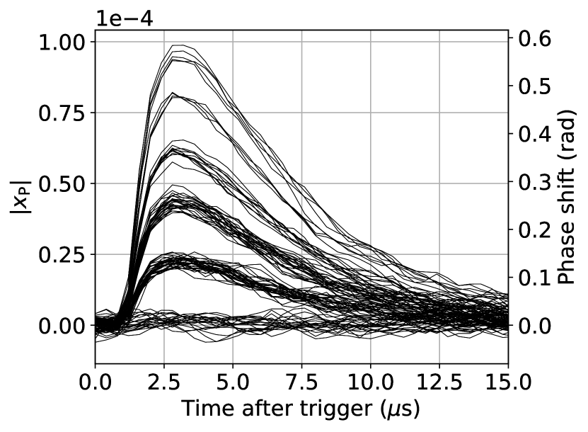
Analogous to the noise data processing, optical pulse events were read out with the homodyne readout, and the I and Q traces were converted to and analyzed in the frequency quadrature. Pulse records processed in this manner are shown in the top panel of Fig. 6, with the pulse height characteristic of the absorbed energy. Here, the traces are clearly separated into discrete groups representing varying numbers of \qty1550nm photons, demonstrating the photon-number-resolving capability of the TES paired with the KICS.
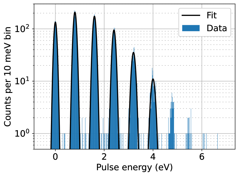
We used the Microcalorimeter Analysis Software Suite (MASS) to further process the pulse records [50]. Here, the traces were optimally filtered [51] to maximize the signal-to-noise ratio (SNR) of the pulse energy estimation. The average pulse trace was combined with photonless noise data to generate the optimal (Wiener) filter. Filtered values representative of the pulse energy were then computed by taking the dot product of each pulse trace with the filter.
The filtered values were energy calibrated using a linear interpolation function generated with the known energies of the first six peaks in the filtered value histogram (zero to five \qty1550nm photons). The energy-calibrated spectrum, shown in the middle panel of Fig. 6, is consistent with a Poisson distribution with . A Gaussian fit was used to extract a FWHM energy resolution of \qty0.137 ±0.001eV at the \qty0.8eV single-photon peak (), comparable to resolutions of similar detectors read out with non-multiplexed DC-SQUIDs [8]. A comparison of energy resolutions up to the 5-photon peak is shown in the bottom panel of Fig. 6. As can be seen, the TES is fairly linear (resolution is roughly flat) across this energy range, but compression begins to degrade the resolution at the higher photon-number peaks.
Discussion
Here, we introduced the principles of the KICS and demonstrated its viability for VNIR TES readout. The kinetic inductance nonlinearity of the KICS largely behaves according to Eqn. 1, and the current sets the responsivity, , and with it the dynamic range of the readout. This is analogous to the inductive coupling in SQUID readouts, although we note with the KICS this can be arbitrarily tuned during cryogenic operation rather than be fixed at fabrication. In this work, a large was chosen to enable high sensitivity to small TES current changes. We also demonstrated KICS self-biasing through a persistent current, useful for reducing pickup from the bias line and readout noise.
With the KICS self-biased, we characterized the VNIR TES readout through IV curve and noise measurements. We observed the readout noise at frequencies of interest (\qty1.4pA/Hz) to be HEMT amplifier limited and considerably below the TES (and filter) noise (\qty21pA/Hz). We then characterized the TES response to \qty1550nm photon pulses and measured a single-photon energy resolution of \qty0.137 ±0.001eV, a value already comparable with DC-SQUID readout. We note that the filter was not well-optimized and added a small but non-negligible amount of noise, but this could be improved with larger . Additionally, the readout noise floor could potentially be reduced by using a nearly quantum-noise limited KITWPA in place of the HEMT amplifer.
Next steps include demonstrating multiplexable readout through a small VNIR TES array read out with multiple KICS devices coupled to a common microwave transmission line. Due to the resonator-based nature of the KICS, we expect this to closely resemble the microwave readouts of MKID arrays [52] and do not anticipate major obstacles. The unique application of persistent currents, however, will need to be further studied to determine the impact on crosstalk between readout channels. Following the readout demonstration, we plan to develop integrated KICS and TES arrays with a targeted 100-m-scale pixel pitch. This will only add a small number of layers to the current TES fabrication process, mainly for the KICS resonators, superconducting switches, and TES shunt and filter resistors. Integrated fabrication will likely be necessary for realizing the dense, kilopixel-scale arrays needed for many astronomy applications, such as exoplanet direct imaging and atmosphere spectroscopy.
As arrays get larger, it would also be useful to individually bias KICS devices in order to tune resonance locations, preventing frequency collisions that reduce yield. In this direction, preliminary work has begun on superconducting bilayer switches fabricated with a thickness ratio and gradient, giving each device a unique temperature at which an optimal can be trapped. Other methods are likely possible though may require increased wiring complexity.
Our work points to another advantage of KICS readout: compatibility with very low circuit inductances. Finite inductance in a TES bias circuit limits TES speed due to the onset of electrothermal instability when the electrical and thermal time constants converge. Here, the circuit inductance was dominated by our conservative choice of , but the limit on inductance is set by which was approximately \qty1nH. In contrast, the use of flux coupling in SQUID circuits necessitates higher inductances in the TES circuit to achieve comparable levels of current noise. Low inductance KICS circuits are particularly well matched to the readout of TESs with sub-microsecond recovery times for continuous-variable photonic quantum computing.
In this work we have demonstrated for the first time a viable alternative readout technology for VNIR TES devices, with a clear path to multiplexed array readout. The KICS could also be extended to other wavelengths and detector technologies. In particular, TES-based x-ray/gamma-ray calorimeters tend to operate at slower timescales than the VNIR TES devices described here. Although SQUIDs provide sufficient readout bandwidth here, the KICS represents a simpler and more scalable alternative that could make large array readout more feasible. Furthermore, the KICS could be used for the readout of MMCs [42], which also use a self-biasing scheme and have historically been limited by the bandwidth of multiplexed SQUID readouts and the noise floor of HEMT amplifiers. Here, the KICS could be especially impactful, particularly if integrated with a quantum-noise-limited KITWPA that shares the same NbTiN material system. Finally, the KICS is not necessarily limited to superconducting detector readout, and any other cryogenic devices requiring sensitive current readout, currently done using a SQUID, could likely be adapted to the KICS.
References
- \bibcommenthead
- [1] Andrews, D. H., Brucksch, W. F., Ziegler, W. T. & Blanchard, E. R. Attenuated Superconductors I. For Measuring Infra-Red Radiation. Review of Scientific Instruments 13, 281–292 (1942).
- [2] Irwin, K. D. & Hilton, G. C. in Transition-Edge Sensors (ed.Enss, C.) Cryogenic Particle Detection, Vol. 99 of Topics in Applied Physics (Springer, Berlin, Heidelberg, 2005).
- [3] Richards, P. L. Bolometers for infrared and millimeter waves. Journal of Applied Physics 76, 1–24 (1994).
- [4] Irwin, K. D., Hilton, G. C., Wollman, D. A. & Martinis, J. M. X-ray detection using a superconducting transition-edge sensor microcalorimeter with electrothermal feedback. Applied Physics Letters 69, 1945–1947 (1996).
- [5] Miller, A. J., Nam, S. W., Martinis, J. M. & Sergienko, A. V. Demonstration of a low-noise near-infrared photon counter with multiphoton discrimination. Applied Physics Letters 83, 791–793 (2003).
- [6] Ullom, J. N. & Bennett, D. A. Review of superconducting transition-edge sensors for x-ray and gamma-ray spectroscopy. Superconductor Science and Technology 28, 084003 (2015).
- [7] Lita, A. E., Miller, A. J. & Nam, S. W. Counting near-infrared single-photons with 95% efficiency. Optics Express 16, 3032–3040 (2008).
- [8] Hummatov, R. et al. Fast transition-edge sensors suitable for photonic quantum computing. Journal of Applied Physics 133, 234502 (2023).
- [9] Smith, D. H. et al. Conclusive quantum steering with superconducting transition-edge sensors. Nature Communications 3, 625 (2012).
- [10] Christensen, B. G. et al. Detection-Loophole-Free Test of Quantum Nonlocality, and Applications. Physical Review Letters 111, 130406 (2013).
- [11] Giustina, M. et al. Significant-Loophole-Free Test of Bell’s Theorem with Entangled Photons. Physical Review Letters 115, 250401 (2015).
- [12] Madsen, L. S. et al. Quantum computational advantage with a programmable photonic processor. Nature 606, 75–81 (2022).
- [13] Rauscher, B. J. et al. ATLAST detector needs for direct spectroscopic biosignature characterization in the visible and near-IR. Proc. SPIE 9602, 96020D (2015).
- [14] Nagler, P. C., Greenhouse, M. A., Moseley, S. H., Rauscher, B. J. & Sadleir, J. E. Development of transition edge sensors optimized for single-photon spectroscopy in the optical and near-infrared. Proc. SPIE 10709, 1070931 (2018).
- [15] Niwa, K., Numata, T., Hattori, K. & Fukuda, D. Few-photon color imaging using energy-dispersive superconducting transition-edge sensor spectrometry. Scientific Reports 7, 45660 (2017).
- [16] Fukuda, D. et al. Confocal Microscopy Imaging with an Optical Transition Edge Sensor. Journal of Low Temperature Physics 193, 1228–1235 (2018).
- [17] Clarke, J. & Braginski, A. I. (eds) The SQUID Handbook: Fundamentals and Technology of SQUIDs and SQUID Systems (Wiley-VCH Verlag GmbH & Co. KGaA, Weinheim, DE, 2004).
- [18] Kiviranta, M., Seppä, H., Van Der Kuur, J. & De Korte, P. SQUID-based readout schemes for microcalorimeter arrays. AIP Conference Proceedings 605, 295–300 (2002).
- [19] Chervenak, J. A. et al. Superconducting multiplexer for arrays of transition edge sensors. Applied Physics Letters 74, 4043–4045 (1999).
- [20] Doriese, W. B. et al. Developments in Time-Division Multiplexing of X-ray Transition-Edge Sensors. Journal of Low Temperature Physics 184, 389–395 (2016).
- [21] Durkin, M. et al. Demonstration of Athena X-IFU Compatible 40-Row Time-Division-Multiplexed Readout. IEEE Transactions on Applied Superconductivity 29, 1–5 (2019).
- [22] Lanting, T. et al. A frequency-domain SQUID multiplexer for arrays of transition-edge superconducting sensors. IEEE Transactions on Appiled Superconductivity 13, 626–629 (2003).
- [23] Akamatsu, H. et al. Progress in the Development of Frequency-Domain Multiplexing for the X-ray Integral Field Unit on Board the Athena Mission. Journal of Low Temperature Physics 199, 737–744 (2020).
- [24] Mates, J. A. B. The Microwave SQUID Multiplexer. Ph.D. thesis, University of Colorado Boulder (2011).
- [25] Mates, J. A. B. et al. Simultaneous readout of 128 X-ray and gamma-ray transition-edge microcalorimeters using microwave SQUID multiplexing. Applied Physics Letters 111, 062601 (2017).
- [26] Ruhl, J. et al. Zmuidzinas, J., Holland, W. S. & Withington, S. (eds) The South Pole Telescope. (eds Zmuidzinas, J., Holland, W. S. & Withington, S.) SPIE Astronomical Telescopes + Instrumentation, 11 (USA, 2004).
- [27] Ade, P. A. R. et al. ANTENNA-COUPLED TES BOLOMETERS USED IN BICEP2, Keck Array , AND SPIDER. The Astrophysical Journal 812, 176 (2015).
- [28] McCarrick, H. et al. The Simons Observatory Microwave SQUID Multiplexing Detector Module Design. The Astrophysical Journal 922, 38 (2021).
- [29] Barret, D. et al. The Athena X-ray Integral Field Unit: A consolidated design for the system requirement review of the preliminary definition phase. Experimental Astronomy 55, 373–426 (2023).
- [30] Szypryt, P. et al. A Tabletop X-Ray Tomography Instrument for Nanometer-Scale Imaging: Demonstration of the 1,000-Element Transition-Edge Sensor Subarray. IEEE Transactions on Applied Superconductivity 33, 1–5 (2023).
- [31] Nakada, N. et al. Microwave SQUID Multiplexer for Readout of Optical Transition Edge Sensor Array. Journal of Low Temperature Physics 199, 206–211 (2020).
- [32] Hayakawa, R. et al. Demonstration of Simultaneous Optical Transition-Edge Sensors Readout Using Microwave SQUID Multiplexer with 5 MHz Flux Ramp Modulation. Journal of Low Temperature Physics (2024).
- [33] Ho Eom, B., Day, P. K., LeDuc, H. G. & Zmuidzinas, J. A wideband, low-noise superconducting amplifier with high dynamic range. Nature Physics 8, 623–627 (2012).
- [34] Malnou, M. et al. Performance of a Kinetic Inductance Traveling-Wave Parametric Amplifier at 4 Kelvin: Toward an Alternative to Semiconductor Amplifiers. Physical Review Applied 17, 044009 (2022).
- [35] Giachero, A. et al. Kinetic Inductance Traveling Wave Amplifier Designs for Practical Microwave Readout Applications. Journal of Low Temperature Physics (2024).
- [36] Kher, A., Day, P. K., Eom, B. H., Zmuidzinas, J. & Leduc, H. G. Kinetic Inductance Parametric Up-Converter. Journal of Low Temperature Physics 184, 480–485 (2016).
- [37] Kher, A. S. Superconducting Nonlinear Kinetic Inductance Devices. Ph.D. thesis, California Institute of Technology (2017).
- [38] Landau, L. D. & Ginzburg, V. L. On the theory of superconductivity. Zhurnal Éksperimental’noĭ i Teoreticheskoĭ Fiziki 20, 1064 (1950).
- [39] Zmuidzinas, J. Superconducting Microresonators: Physics and Applications. Annual Review of Condensed Matter Physics 3, 169–214 (2012).
- [40] Day, P. K., LeDuc, H. G., Mazin, B. A., Vayonakis, A. & Zmuidzinas, J. A broadband superconducting detector suitable for use in large arrays. Nature 425, 817–821 (2003).
- [41] Gao, J. The Physics of Superconducting Microwave Resonators. Ph.D. thesis, California Institute of Technology (2008).
- [42] Kempf, S., Fleischmann, A., Gastaldo, L. & Enss, C. Physics and Applications of Metallic Magnetic Calorimeters. Journal of Low Temperature Physics 193, 365–379 (2018).
- [43] Szypryt, P. et al. Large-format platinum silicide microwave kinetic inductance detectors for optical to near-IR astronomy. Optics Express 25, 25894 (2017).
- [44] Vissers, M. R. et al. Frequency-tunable superconducting resonators via nonlinear kinetic inductance. Applied Physics Letters 107, 062601 (2015).
- [45] Sauvageau, J. et al. Superconducting integrated circuit fabrication with low temperature ECR-based PECVD SiO2 dielectric films. IEEE Transactions on Appiled Superconductivity 5, 2303–2309 (1995).
- [46] Durkin, M. et al. Physical Neighbor Crosstalk in Time Division Multiplexed SQUID Arrays for TES Readout. Journal of Low Temperature Physics (2024).
- [47] Staguhn, J. et al. Design of Large Low Noise Transition Edge Sensor Arrays for Future FIR Space Missions. Journal of Low Temperature Physics (2024).
- [48] Lita, A. et al. Tuning of Tungsten Thin Film Superconducting Transition Temperature for Fabrication of Photon Number Resolving Detectors. IEEE Transactions on Appiled Superconductivity 15, 3528–3531 (2005).
- [49] Miller, A. J. et al. Compact cryogenic self-aligning fiber-to-detector coupling with losses below one percent. Optics Express 19, 9102 (2011).
- [50] Fowler, J. W. et al. The Practice of Pulse Processing. Journal of Low Temperature Physics 184, 374–381 (2016).
- [51] Szymkowiak, A. E., Kelley, R. L., Moseley, S. H. & Stahle, C. K. Signal processing for microcalorimeters. Journal of Low Temperature Physics 93, 281–285 (1993).
- [52] Fruitwala, N. et al. Second generation readout for large format photon counting microwave kinetic inductance detectors. Review of Scientific Instruments 91, 124705 (2020).
Methods
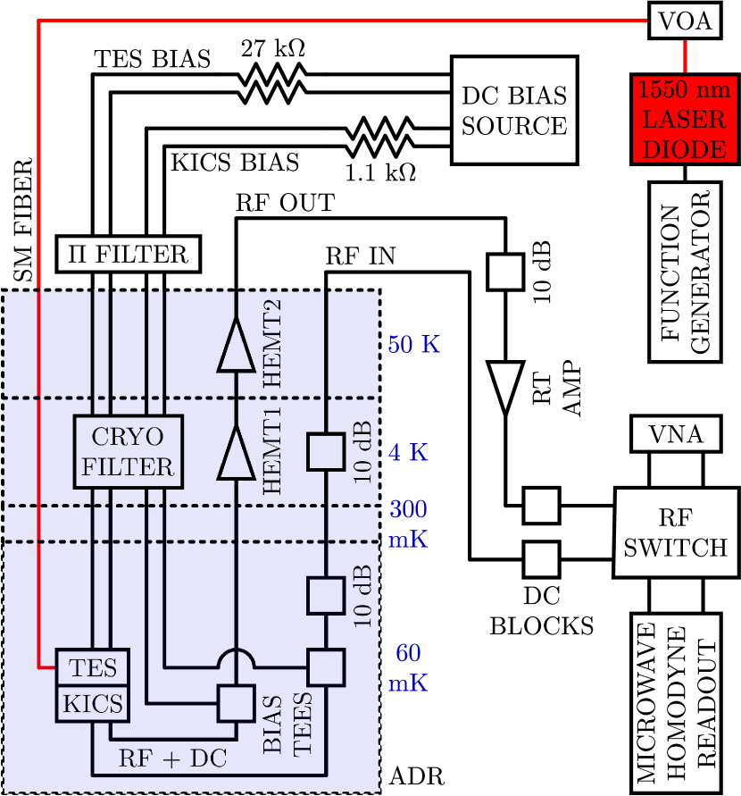
A schematic of the overall experimental setup is shown in Extended Data Fig. 1. An ADR backed by a He-3 sorption cooler was used to perform the measurements, with the KICS and VNIR TES typically controlled at \qty60mK. The cryostat contains 4 main temperature stages, with temperatures of \qty60mK, \qty300mK, \qty4K, and \qty50K. The experimental setup can roughly be divided into three categories/circuits: optical, DC, and RF. These are described in more detail below.
Optical pulses are created by a \qty1550nm laser diode actuated with a pulse mode function generator, enabling nanosecond-scale photon pulses. The optical output of the laser diode is connected to a variable optical attenuator (VOA), allowing control of the mean photon number in optical pulses. Single-mode (SM) fiber with a core diameter of \qty9μm is used to couple the output of the VOA to the VNIR TES inside the cryostat. At each of the temperature stages, the optical fiber is heat sunk to the stage and coiled to filter black-body radiation that couples in from the room temperature side of the fiber. The fiber is terminated with a ferrule and connected to a ZrO2 mating split sleeve. The TES chip is micromachined into a circular shape with diameter matching the ZrO2 sleeve inner diameter and mounted on a sapphire rod of the same diameter within the device box. The ZrO2 sleeve containing the fiber ferrule is inserted over the TES and sapphire rod, self-aligning the TES to the fiber core. The TES uses Nb leads that extend out through the ZrO2 split sleeve gap, enabling wire bonding to the device.
A multi-channel digital-to-analog converter (DAC) was used as the DC bias source for the KICS (generating persistent current) and TES. Bias resistors of \qty1.1kΩ and \qty27kΩ were placed at the DAC outputs to be able to source appropriate current levels for the KICS and TES, respectively. The DC bias was applied differentially and symmetrically, and twisted pair wiring was used to mitigate electronics noise and pickup. To further reduce noise, the DC lines were low-pass filtered at three locations. This includes a \qty10Hz filter internal to the DAC, a \qty4nF pi filter (\qty800kHz cut-off) at the cryostat feedthrough, and cryogenic filter banks (\qty65kHz cut-off for lowest frequency bank) at the \qty4K stage. To couple DC current through the RF microstrip line and into the KICS resonator, a set of bias tees on the \qty60mK stage was used.
The RF circuit contains the hardware needed to drive and read out the KICS resonator, connected via coaxial cabling. The RF input to the cryostat consists of \qty10dB attenuators on the \qty4K and \qty60mK stages, used to reduce the noise of the room temperature probe tone before reaching the \qty60mK device input. The RF output from the device is first amplified at the \qty4K stage by a commercial HEMT amplifier (HEMT1) with a specified noise temperature and gain of \qty25dB at \qty4GHz. The output is further amplified at the \qty50K stage by a second HEMT amplifier (HEMT2). Outside the cryostat, a \qty10dB attenuator and a room temperature amplifier (RT AMP) are used to adapt to power levels that are suitable for the room temperature readout electronics. DC inner/outer blocks are used to isolate the cryostat and electronics low frequency signals and grounds. Device characterization measurements are performed using a commercial VNA and a custom microwave homodyne readout system, with a RF switch used to choose between the two.
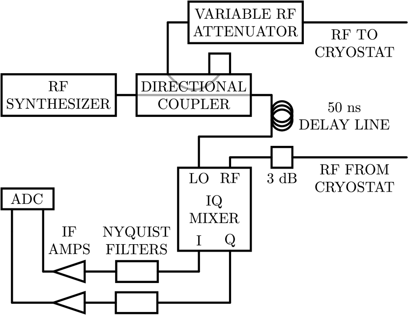
A schematic of the microwave homodyne readout is shown in Extended Data Fig. 2. A RF synthesizer is used to generate a probe tone at the KICS resonant frequency. A directional coupler is used to split this waveform, with one portion sent to the local oscillator (LO) port of an IQ (in-phase and quadrature) mixer. The other portion is sent through a variable RF attenuator and the KICS device in the cryostat before arriving at the RF port of the IQ mixer. A \qty50ns delay line is added in front of the LO port in order to mitigate effects of the cable delay in the I and Q outputs. The I and Q outputs are filtered with \qty1MHz cut-off Nyquist filters. Intermediate frequency (IF) amplifiers are used to amplify the I and Q signals to utilize the full range of an analog-to-digital converter (ADC). This 14-bit ADC is used to digitize the I and Q signals at a \qty2.5MHz sampling rate.
Data availability All data used in this study are available from the corresponding author upon reasonable request.
Code availability
The Microcalorimeter Analysis Software System (MASS) code used to analyze the data in this work is available via GitHub at https://github.com/usnistgov/mass. All other code is available from the corresponding author upon reasonable request.
Acknowledgements
This work was supported by the NASA APRA program under Grant No. NNH23OB118A. AG is supported by the European Union’s H2020-MSCA under Grant No. 101027746. Certain commercial equipment, instruments, or materials are identified in this paper in order to specify the experimental procedure adequately. Such identification is not intended to imply recommendation or endorsement by the National Institute of Standards and Technology, nor is it intended to imply that the materials or equipment identified are necessarily the best available for the purpose.
Author contributions
P.S., D.A.B, S.N., G.C.O., D.S.S., J.N.U., M.R.V., and J.G. conceptualized and developed the work. A.G, A.E.L, and J.G. simulated and designed the KICS and TES devices. M.R.V and A.E.L fabricated the KICS and TES devices. P.S., J.W.F., R.H., G.C.O., J.W., and J.G. developed the experimental hardware and analysis tools. P.S. and I.F. conducted the experiments. P.S and J.A.B.M. analyzed the data. P.S. wrote the manuscript. All authors reviewed the manuscript.
Competing interests
The authors declare no competing interests.