Tuning monolayer superconductivity in twisted NbSe2 graphene heterostructures
Abstract
The recent advent of artificial structures has triggered the emergence of fascinating phenomena that could not exist in natural compounds. A prime example is twisted multilayers, i.e., superlattices represented by magic-angle twisted bilayer graphene (MATBG). As in the case of MATBG, unconventional band hybridization can induce a new type of superconductivity: artificial band engineering by twist induces properties different from the original systems. Here, we apply this perspective to a monolayer superconductor NbSe2 stacked with a twist on doped graphene. We show that the superconducting states of the NbSe2 layer change dramatically by varying the twist angle. Our result shows that twist tuning, in addition to substrate effects, will provide a strategy for designing monolayer superconductors with high controllability.
I INTRODUCTION
Exploration of unconventional superconductivity has been a central topic of condensed matter physics for a long time. Lower dimensionality has been thought of as one way to tackle this problem Saito et al. (2016a); Brun et al. (2016); Qiu et al. (2021). This kind of belief contributed to the development of nanotechnology, and as technology progressed in a top-down direction, many nontrivial phenomena were found by thinning, depositing and interfacing materials Ohtomo and Hwang (2004); Gupta et al. (2015); Gariglio et al. (2015); Wang et al. (2016); Tan et al. (2013); Liu et al. (2012); He et al. (2013); Xiang et al. (2012). For example, many researchers have focused on transition metal dichalcogenides (TMD) belonging to van der Waals (vdW) materials Mak et al. (2010); Ye et al. (2012); Voiry et al. (2015); Wang et al. (2012); Han et al. (2018); Devarakonda et al. (2020); Ding et al. (2011). The vdW materials have layered structures and can be exfoliated easily. This allowed for controlling on the atomic scale, which led to investigation and clarification of monolayer superconductivity.
Some hexagonal TMD such as NbSe2, TaS2, and doped MoS2 are known to exhibit superconductivity from bulk to even monolayer Ye et al. (2012); Xi et al. (2015); Costanzo et al. (2016); Saito et al. (2016b); Navarro-Moratalla et al. (2016); Peng et al. (2018). In particular, monolayer NbSe2 is intrinsically metallic and becomes a multigap superconductor with Fermi surfaces around the K valley and around the point Yokoya et al. (2001); Khestanova et al. (2018); Dvir et al. (2018); Wickramaratne et al. (2020); Noat et al. (2015); Zheng and Feng (2019). In addition, hexagonal TMD have in common a strong spin-orbit coupling (SOC), so-called Ising SOC, in the monolayer limit due to the spatial inversion symmetry breaking. This causes spin-momentum locking, and therefore the superconducting (SC) pairing is extremely robust to external in-plane magnetic fields Xi et al. (2016); Saito et al. (2016b); Lu et al. (2015); Wang et al. (2017); Ugeda et al. (2016); de la Barrera et al. (2018); Xing et al. (2017); Wan et al. (2022); Navarro-Moratalla et al. (2016); Costanzo et al. (2016). The robustness of such a SC state to magnetic fields makes them crucial both from a fundamental point of view and for possible applications.
On the other hand, subsequently, many attempts have been made in a bottom-up direction recently, i.e., stacking materials to create a superlattice by replacing, alternating, or twisting layers Naritsuka et al. (2021); Goh et al. (2012); Shishido et al. (2010); Mizukami et al. (2011); Niu and Li (2015); Kim et al. (2016); Veneri et al. (2022); Nie et al. (2023); Li and Koshino (2019); Xiao et al. (2023); Dreher et al. (2021); Geim and Grigorieva (2013); Kennes et al. (2021); Behura et al. (2021); Liao et al. (2019); Tran et al. (2020). Notably, there has been intense research on physics in twisted vdW bilayers in the last five years. In 2018 discovery of superconductivity in magic-angle twisted bilayer graphene (MATBG) marked a milestone Cao et al. (2018a, b), which drew a great deal of attention to the superconductivity as the first emerging by the twist Yankowitz et al. (2019); Tarnopolsky et al. (2019); Andrei and MacDonald (2020); Ramires and Lado (2018); Qin and MacDonald (2021); Ray et al. (2019); Scheurer and Samajdar (2020); Peltonen et al. (2018); Christos et al. (2023); Oh et al. (2021); Wu et al. (2018); Po et al. (2018); Isobe et al. (2018); Saito et al. (2020); Arora et al. (2020); González and Stauber (2019); Codecido et al. (2019); Kerelsky et al. (2019). As represented by the flat band in MATBG, the most valuable aspect of the structures is the control of band hybridization by the twist angle Lisi et al. (2021); Suárez Morell et al. (2010); Zhang et al. (2020); Devakul et al. (2021); Xian et al. (2021). This means that artificial band engineering is possible with the control of experimental parameters. Furthermore, twisted heterostructures are expected to induce novel physical properties due to a wider range of material selection compared to structures of the same materials Veneri et al. (2022); Nie et al. (2023); Li and Koshino (2019); Xiao et al. (2023); Dreher et al. (2021); Geim and Grigorieva (2013); Kennes et al. (2021); Behura et al. (2021); Liao et al. (2019); Tran et al. (2020). This indicates that electronic states suitable for unusual superconductivity could be extracted by combining selected properties of different materials.
As previous studies without a twist, a monolayer FeSe on SrTiO3 substrate has been found to exemplify high-temperature superconductivity by the combination of properties of FeSe monolayer and the substrate effect Tan et al. (2013); Liu et al. (2012); He et al. (2013); Xiang et al. (2012). Nevertheless, the modulation of the intrinsic SC property is not yet well understood in twisted heterostructures of monolayer superconductors and other materials. A monolayer superconductor stacked with a twist on a monolayer substrate is regarded as a twisted bilayer, in which the monolayer SC state is expected to be strongly tuned by the substrate. Especially when the substrate is metallic, band hybridization near the Fermi level could modulate the monolayer SC states. In addition, the presence of an experimental parameter, i.e., the twist angle, can make it possible to design physical properties infeasible so far. Therefore, tuning monolayer SC states enabled by substrate effects and twist has the potential to induce unconventional phenomena on a monolayer superconductor such as the enhancement of transition temperature, topological superconductivity, and SC diode effect Tan et al. (2013); Liu et al. (2012); He et al. (2013); Xiang et al. (2012); Zhang et al. (2018); Machida et al. (2019); He et al. (2018); Kezilebieke et al. (2020); Xie and Law (2023).
In this paper, we investigate the property of monolayer superconductivity, especially in a monolayer NbSe2 stacked with a twist on doped graphene. The doped graphene is treated as a metallic substrate. We then regard this system as a twisted bilayer and identify each as a top and bottom layer. The previous work revealed that there are two scenarios of band hybridization because of a large mismatch of lattice constants and significant difference in the size of Fermi surfaces in twisted NbSe2 graphene heterostructures Gani et al. (2019). Moreover, they showed that SC pairing could be induced into the graphene layer by proximity effect, but the details of SC states in the NbSe2 layer are not paid attention to and uncovered. In this paper, we focus on the property of the NbSe2 layer and reveal its twist angle dependence. In superlattices, interlayer band hybridization and long periodicity in real space can affect superconductivity. We mainly focus on the former effect and construct an effective model based on which we theoretically treat the multigap superconductivity for arbitrary twist angles.
II FORMULATION
First, we explain the formulation of this work. The previous work Gani et al. (2019) mainly focused on graphene and adopted a continuum model Mele (2010); Bistritzer and MacDonald (2011); Koshino and Nam (2020); Lopes dos Santos et al. (2007). However, due to the large lattice mismatch, it is not adequate for the analysis of the angle dependence of SC states. Alternatively, we here consider a generalized Umklapp process for general commensurate or incommensurate bilayers Koshino (2015); David et al. (2019). Then, we build a model focusing on the low-energy states because only the low-energy electronic states near the Fermi level are important for superconductivity.
II.1 Low-energy effective model of each layer
Before constructing an entire Hamiltonian describing NbSe2 graphene heterostructures, we introduce the electronic structure of each layer and show the intralayer Hamiltonian for the low-energy effective model. In this paper, we use the parameters evaluated in Ref. Gani et al., 2019.
We write the primitive lattice vectors as for the NbSe2 layer and for the graphene layer, which are all oriented in-plane direction. The reciprocal lattice vectors are written as and for NbSe2 and graphene layers respectively, to satisfy . In the same way, other physical quantities of NbSe2 and graphene layers shall be distinguished with or without a tilde.
In graphene, the carbon atoms form a honeycomb lattice with two sublattices, which are specified by . The lattice constant is =2.46 Å. Here, we choose the primitive lattice vectors , and primitive reciprocal lattice vectors and . Thus, the lattice positions are given by
| (1) |
where are integers and , are positions of sublattices.
The low-energy states are located near the valley points of Brillouin zone (BZ) , where labels the valley degree of freedom (DOF). The single-particle Hamiltonian around these valleys is described by massless Dirac fermions
| (2) | ||||
| (3) |
where are the labels of up spin and down spin, is the wave vector measured from each valley point, means an identity matrix in spin space, is Fermi velocity, is a chemical potential of graphene, and are Pauli matrices representing the sublattice DOF. () is the creation (annihilation) operator of a low-energy electron around each valley. It is convenient to define the following spinor for each valley:
| (4) |
Similarly, the H-type NbSe2 also forms a honeycomb lattice with which a sublattice consists of one Nb atom and two Se atoms. The Se atoms symmetrically displace above and below the plane formed by the Nb atoms (Fig. 1). The lattice constant is =3.48 Å and primitive lattice vectors , primitive reciprocal lattice vectors , and positions of the K valley points are obtained by replacing in those of graphene. The BZ is also hexagonal, and in contrast to graphene the Ising SOC results in a spin splitting of Fermi Surfaces (FSs), which conserve spin .
Unlike graphene, the low-energy states are located around both the K valleys and the point. In the monolayer limit, only the orbitals of Nb atoms contribute to the low-energy states. This fact allows us to consider only the Nb sublattice DOF as long as our focus is limited to the low-energy region. The effective models for electrons around the point and the valleys are as follows:
| (5) | ||||
| (6) | ||||
| (7) | ||||
| (8) |
where
| (9) | ||||
| (10) |
Like the Hamiltonian of graphene, is measured from the or points. Here, () is the creation (annihilation) operator for an electron on NbSe2. It is worth mentioning again that we ignore the sublattice DOF of Se atoms. We also define the following spinors for NbSe2 low-energy states:
| (11) | ||||
| (12) |
Hereafter, all wave vectors are normalized by the unit length in reciprocal space of NbSe2 . The parameters of the above effective models are shown in Table 1. Note that graphene is doped in the heterostructure () Gani et al. (2019), making the graphene metallic substrate.
| 0.5641 | 0.5085 | 0.4526 | 3.07 | 0.0707 | -0.33 |
II.2 General theory for misoriented bilayers
Figure 1 shows the considered setup in this paper. The monolayer NbSe2 is stacked on graphene, and the top layer is twisted counterclockwise by relative to the bottom layer. This means at the same time that the graphene layer is twisted by to the NbSe2 layer. Hence, we regard this system as one in which the NbSe2 layer is fixed and the graphene layer is twisted in the clockwise direction with twist angle . Accordingly, vectors of the graphene layer in both real and reciprocal space are transformed such as , , where
| (13) |
is the rotation matrix and we use . Other vectors follow the same transformation, and in the following, characters with tildes implicitly represent vectors undergone a rotational transformation.
The entire Hamiltonian for twisted heterostructures is the sum of the above intralayer Hamiltonian and an interlayer hopping term, written as . and are the intralayer Hamiltonian of graphene and NbSe2 mentioned in the previous subsection.
The interlayer coupling is small enough to be treated as a perturbation compared to the energy scales of in this system. This is a consequence of the large lattice mismatch, in addition to the fact that bilayers are connected by weak vdW forces Gani et al. (2019); Lopes dos Santos et al. (2007); Zhang et al. (2014). Therefore, we adopt a theory for general misoriented bilayers Koshino (2015). In this scheme, an electronic state with a Bloch wave vector of the NbSe2 layer and that of the graphene layer with are coupled only when where and are reciprocal lattice vectors of each layer. In other words, the neighboring layers’ states are coupled at common wave vectors in the extended BZ scheme. Instead, however, it could be considered that the states of graphene with couple to the states with in the first BZ of NbSe2 in the reduced zone scheme. Thus, we construct a model by adopting the latter interpretation.
The interlayer Hamiltonian is written as
| (14) |
where
| (15) |
and is the amplitude of the coupling which decays dramatically in large . Therefore, we merely consider a limited number of components in the summation of Eq. (15) and ignore graphene valleys except for the innermost valleys in the extended zone scheme.
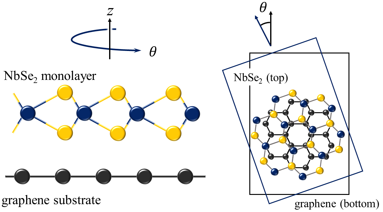
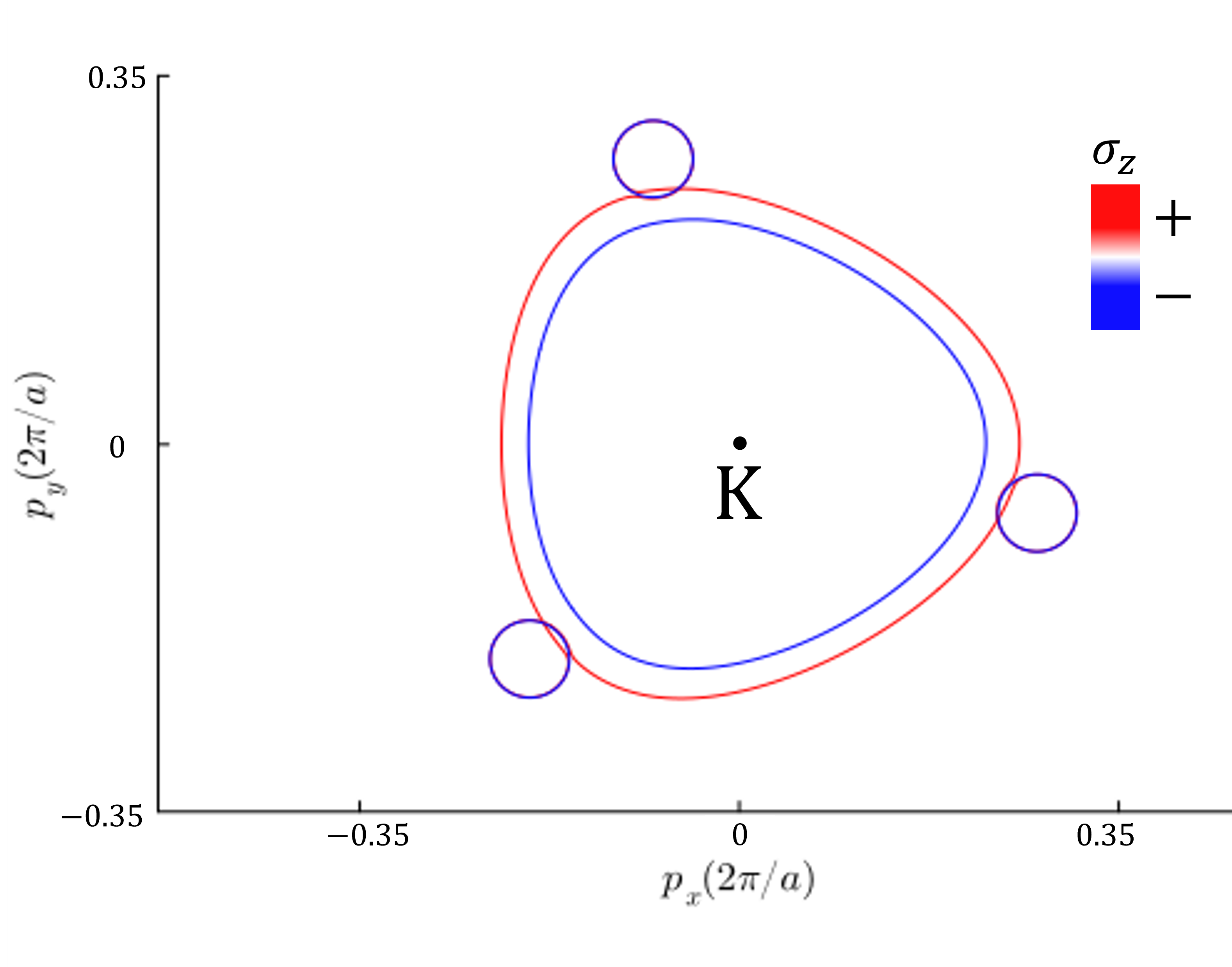
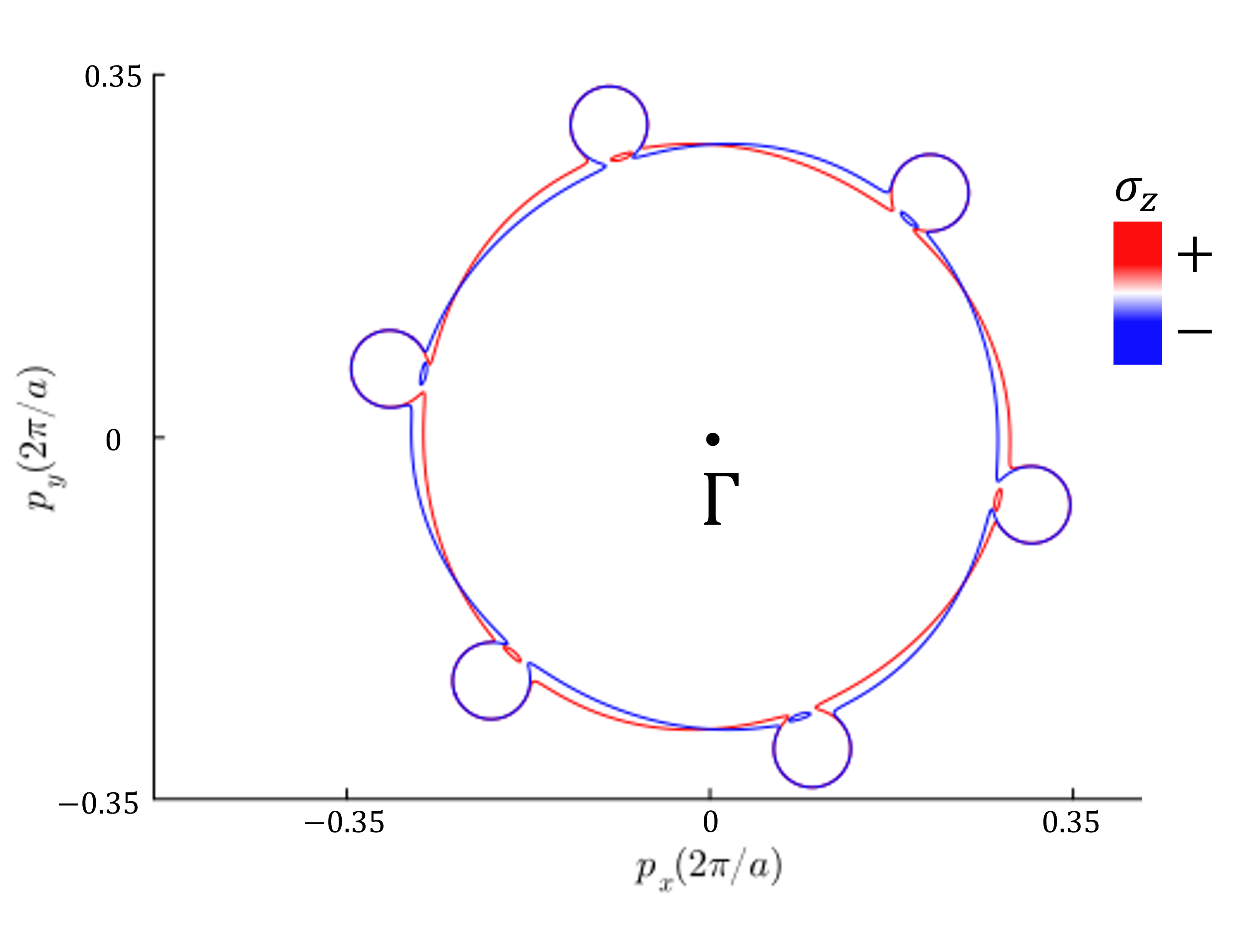
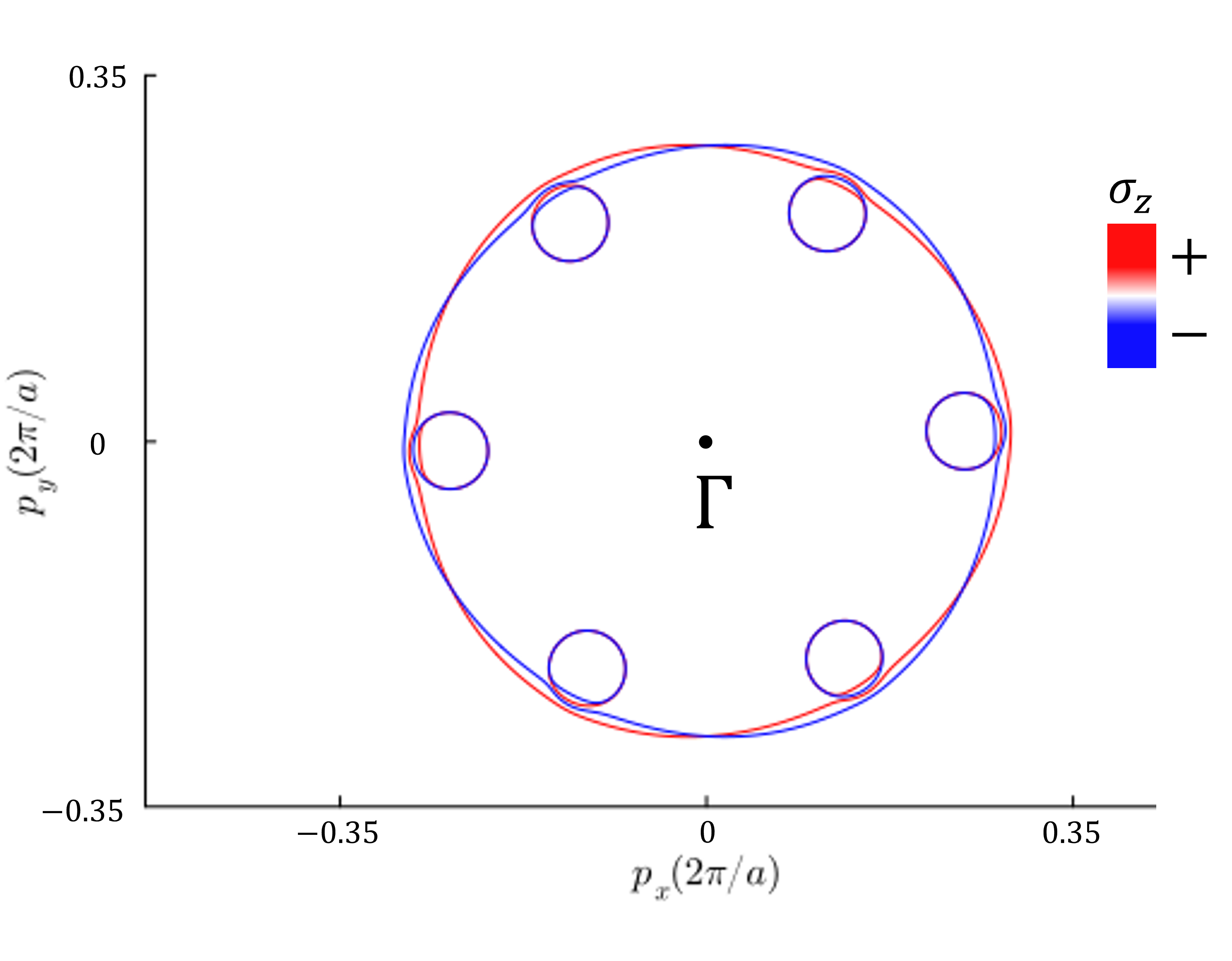
Figure 2 illustrates the FSs of layers in the extended zone scheme and corresponding positions inside the first BZ of NbSe2 for , for example. There are two scenarios of hybridization between the graphene and NbSe2 FSs. When the twist angle is small , the graphene and NbSe2 FSs around each K valley hybridize. On the other hand, the graphene FSs around valleys hybridize the NbSe2 FS around the point, when the twist angle is large . Owing to the symmetry of reciprocal space, we can restrict the twist angle as .
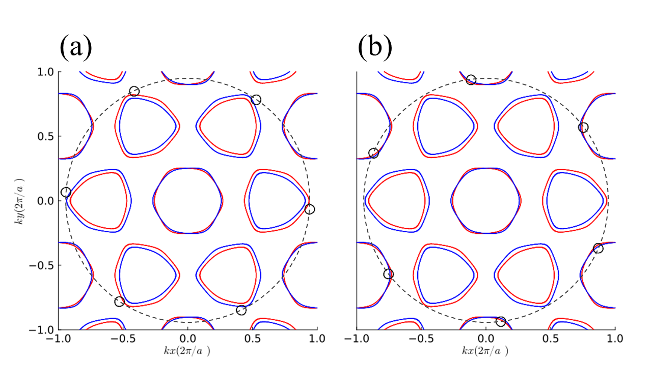
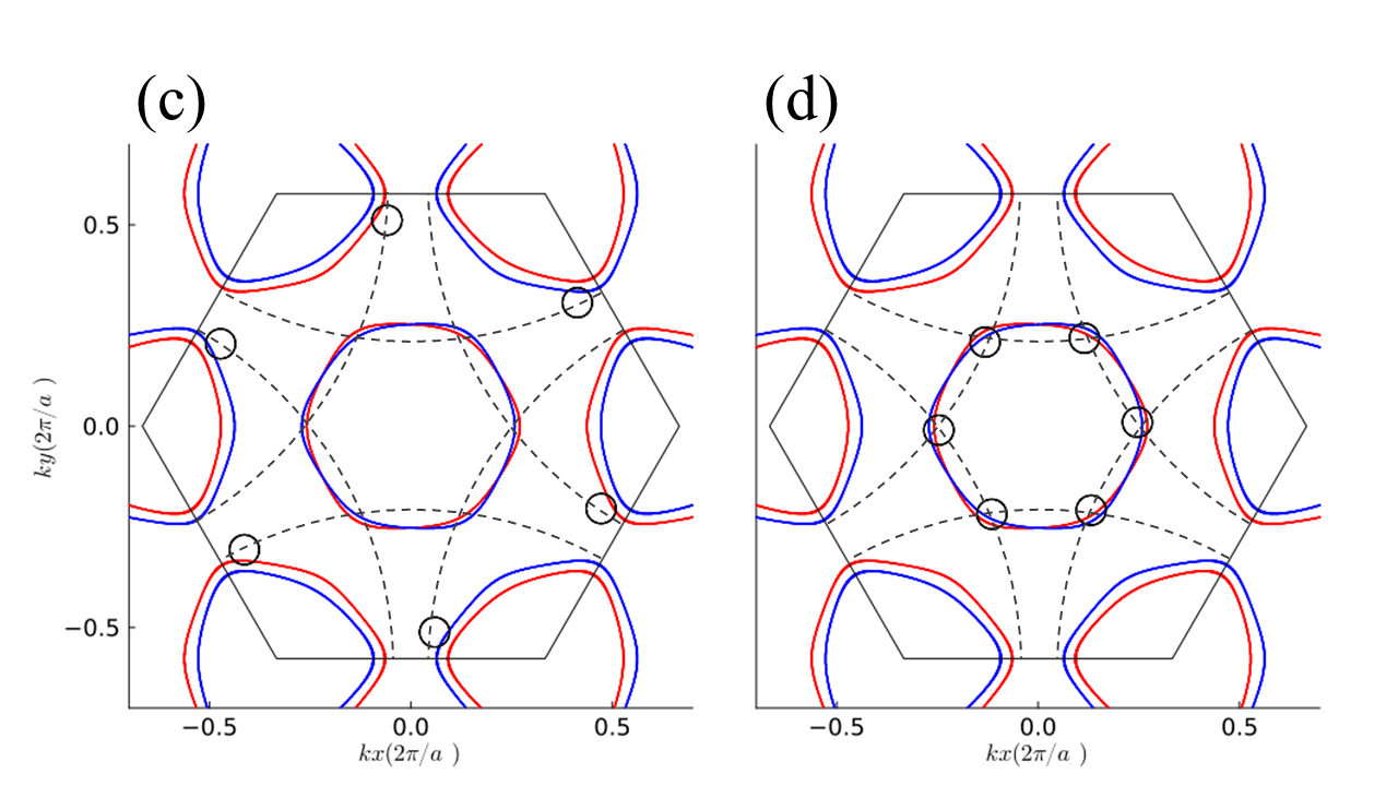
First, we consider the case of a small twist angle around . In this case, valleys of the same sign in each layer are hybridized, i.e., . Let us ignore the FS around the point of NbSe2 for simplicity because it is hardly affected by band hybridization. Under this assumption, we can describe the low-energy states around the valley of each sign simply by considering the Bloch basis of NbSe2 and three equivalent bases for graphene. In addition, the offset vectors between and are naturally derived from Eq. (15). The summation over is restricted to three vectors , , and . Similarly, the sum over could be restricted as , , and . Therefore, the three offset vectors for each valley become as follows:
| (16) |
Because of the relationship , we can rewrite by defining . It should be noticed that depend on the twist angle .
The wave number in NbSe2 is coupled to in graphene as mentioned above. Hence, in NbSe2 and in graphene are coupled, where is the wave vector measured from or . The interlayer Hamiltonian between these states is written as Zhang et al. (2014)
| (17) |
where
| (18) | ||||
and we here use , , . In this paper, we adopt meV as an interlayer hopping energy Gani et al. (2019). Therefore, the entire effective Hamiltonian of the twisted heterostructure describing the low-energy states around each valley is obtained as
| (19) |
where
| (20) |
and we define the following spinor for simple notation:
| (21) |
Next, we consider the case where is around . The interlayer Hamiltonian can be formulated in the same way as in the former case, but the two K valleys of graphene can not be considered independently because both valleys hybridize the FS of NbSe2 around the point. Moreover, we have to redefine the three offset vectors. In this case, are the same as those of the aforementioned case. However, the restricted change as , , and , and the offset vectors between and become where
| (22) |
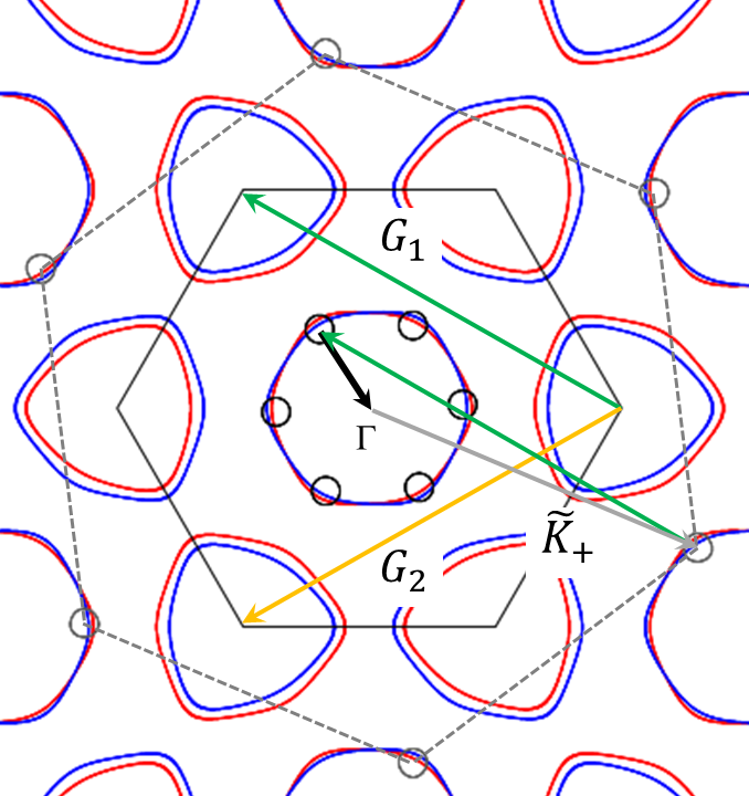
For example, Fig. 3 shows the offset vector in addition to other vectors for . We depict a representative offset vector by the black arrow. In Fig. 3, we see the necessity for considering the two valley FSs of graphene. Thus, the basis function is spanned by those of NbSe2 and valleys of graphene with . The entire Hamiltonian for the low-energy states around the point is
| (23) |
where and are the following matrix and spinor:
| (24) |
| (25) |
II.3 Mean field approximation
NbSe2 exhibits superconductivity regardless of the number of layers, from monolayer to bulk. In contrast, monolayer graphene still be a normal metal down to low temperatures. Thus, we assume that the pairing interaction for superconductivity is present only in the NbSe2 layer. Moreover, simple s-wave superconductivity due to electron-phonon coupling is assumed. Hereafter, we focus on the change of monolayer SC properties by band hybridization, and qualitative properties are expected to be independent of the symmetry of superconductivity.
The paring interaction Hamiltonian for NbSe2 is written as
| (26) |
In SC states, the expectation value is nonzero, and the order parameter is defined by
| (27) |
In the mean field approximation, the four-body operator of is approximated by two-body operators, and the pairing interaction Hamiltonian is simplified by the following mean field Hamiltonian:
| (28) |
Finally, consistent with the assumption of s-wave superconductivity, the pairing interaction has the form,
| (29) |
The presence of multiple FSs around the valleys and the point in the NbSe2 layer lead to multigap superconductivity. The simplest formalism deals with independent Cooper pairings on each FS by considering three distinct electron-phonon coupling amplitudes (see Fig. 4). The order parameter on the FS is
| (30) |
Similarly, the Cooper pairing between the and valleys are defined by the following order parameters,
| (31) | ||||
| (32) |
Note that the two order parameters , are considered because of spin splitting by the Ising SOC. The schematic image of the above three Cooper pairings is shown in Fig. 4.
We introduce the following Nambu spinors for each FS:
| (33) | ||||
| (34) |
When the FSs of NbSe2 and graphene around the K valleys are hybridized with each other, the Bogoliubov de Gennes (BdG) Hamiltonian describing the SC states is a sum of , , and . If we ignore the FS around , the pairing interaction Hamiltonian under the mean field approximation becomes
| (35) |
Therefore, the BdG Hamiltonian is written as
| (36) |
where
| (37) |
is a matrix in Nambu space and
| (38) |
It is noteworthy that the sign of the valley used for can be restricted to either or . We have ignored the FS around the point in this formulation, but it can be straightforwardly extended by adding the monolayer BdG Hamiltonian for the FS around to .
In the same way, the BdG Hamiltonian is obtained as follows, when the FSs around the point hybridize the FSs of graphene:
| (39) |
where
| (40) | ||||
| (41) |
II.4 Self-consistent gap equation for NbSe2 layer
In the previous subsection, we constructed the BdG Hamiltonian for the SC states. As the next process, here we shall derive self-consistent gap equations for the SC states Sato and Ando (2017).
In general, a matrix of the BdG Hamiltonian can be diagonalized as
| (42) |
with a unitary matrix
| (43) |
where and run from to , and the eigenvalue equation
| (44) |
is satisfied for the -th eigen state. We define new creation/annihilation spinors for Bogoliubov quasiparticles as
| (45) |
Here, corresponds to either of or . In this diagonalized basis, the BdG Hamiltonian is written as
| (46) |
Thus, the expectation values of are
| (47) |
where is the Fermi distribution function, and other expectation values such as equal 0.
In the remaining part, the self-consistent gap equations are derived. The first and second components of are the operators of electrons on the NbSe2 layer. Thus, from corresponding equations in Eq. (45):
| (48) | ||||
| (49) |
the gap equations in Eqs. (30), (31), and (32) can be represented by the thermal distribution of Bogoliubov quasiparticles. For instance, in the case of the pairing around the point, Eq. (30) becomes
| (50) |
where we used the expectation values in Eq. (47). Note that and are determined by the BdG Hamiltonian and depend on . Thus, we can obtain the order parameter by solving the gap equation Eq. (50) self-consistently. Similarly, the gap equations for the order parameters around the K valleys are obtained by
| (51) | ||||
| (52) |
In general, only the electronic states near the Fermi level contribute to the SC states. Therefore, the summation of wave numbers is restricted to the low-energy region by introducing an energy cutoff that corresponds to the Debye frequency. In this paper, we set the Debye frequency of NbSe2 as meV Eremenko et al. (2009), and the sum of wave numbers in Eqs. (50), (51), and (52) are implicitly restricted to the energy window from the Fermi level.
III Results
III.1 Twist angle dependence of SC states
We here compare the superconducting properties in the present twisted bilayer with those of the monolayer NbSe2. For a model of the monolayer NbSe2, we set meV where the twisted bilayer is decoupled. We can deduce the properties of the monolayer NbSe2 in this setup and compare the results with those of meV for the twisted bilayer.
We first discuss the SC gap functions , and . Figure 5 shows the twist angle dependence of the gap functions compared to that of the monolayer. The temperature of the system is fixed to zero temperature . Here, we set the interaction parameters as , , so that the transition temperature in the decoupled limit coincides with the experimental value of monolayer NbSe2, K. Note that the amplitude of the s-wave gap is plotted only for angles due to the symmetry of the system Gani et al. (2019). On account of the band hybridization between the SC layer and the normal metallic layer, the SC gap function around the K valleys diminishes drastically for , although it almost coincides with the monolayer for angles around . In contrast, decreases for . These behaviors are consistent with the fact that the FSs of graphene are hybridized with the FSs of NbSe2 around the K valleys near while with those around the point near .

The suppression of superconductivity can be attributed to the decrease in the density of states (DOS) near the Fermi level. In the vicinity of the band crossing points of the twisted heterostructure, the graphene states and the NbSe2 states within the finite energy window hybridize, resulting in a band gap opening. The gap opening around the Fermi level decreases the low-energy DOS and suppresses the SC states. Consistent with this view, suppression of the SC gap in NbSe2 is maximized at certain twist angles. That is, is minimized at , and is minimized at and . For these angles, the FSs of graphene and NbSe2 strongly overlap (see Figs. 6, 7, and 8), which supports the above interpretation. This result is slightly different from the behavior of the induced SC gap on the graphene layer studied in Ref. Gani et al., 2019, although these phenomena have a common origin.
We next focus on the details of SC gap tuning by the bilayer coupling. In the previously shown Fig. 5, we fixed the temperature K, and the interlayer hopping term was either meV or meV. Alternatively, we here fix the twist angle as , , where the SC gap is significantly suppressed, and vary the interlayer coupling . The temperature dependence of the SC gap is shown in Fig. 9, in which we see that the superconductivity of NbSe2 is monotonically suppressed as the interlayer coupling increases. This suppression originates from the expansion of the band gap by which the DOS becomes smaller than that of the monolayer system.
Interestingly, from Fig. 5 we can see that the SC gap of NbSe2 can be enhanced by twisting under a certain condition, in contrast to the above cases. For instance, is larger than that of the decoupled system. Similarly, and are also enhanced at certain twist angles. The enhancement of superconductivity by hybridization with a normal metal is counterintuitive. However, we can reveal the mechanism of enhanced superconductivity by discussing the DOS in the normal states (see next subsection).
Finally, we discuss the contrasting behaviors of and . Although the spin-split K valleys of monolayer NbSe2 have nearly the same SC gaps, they can differ significantly in the twisted bilayer. For example, around . The difference in the SC gap functions can be regarded as parity mixing in Cooper pairs. In the two-band model, the SC gaps of two spin-split FSs are given by , where () is the order parameter of spin-singlet (spin-triplet) superconductivity Bauer and Sigrist (2012). Thus, inequivalence between and indicates the significant parity mixing by twisting. We find it interesting that the spin-triplet Cooper pairs can be induced in a controllable way by twisting.
III.2 Density of states on normal NbSe2 layer
To clarify the enhancement of superconductivity in the twisted bilayer, we calculate the DOS in the normal state. Because NbSe2 is an intrinsic superconductor while graphene is not, we consider the DOS contributed from the NbSe2 layer, not the total DOS of the twisted heterostructure. We then define the spectral function and the DOS contributed from the NbSe2 layer as Koshino (2015)
| (53) | ||||
| (54) |
where is an index of spin, is an energy from the Fermi level, are energy eigenvalues of the Hamiltonian in Eqs. (20) and (24), and is the total amplitudes of spin on the NbSe2 layer in the eigen state of . Below we show the DOS in the effective Hamiltonian Eqs. (20) and (24), in which we focus on the specific FSs around the K point or point. Therefore, discussed below corresponds to the partial DOS. For instance, in the case of the effective Hamiltonian for the K valleys Eq. (20), the DOS of the spin up/down bands is calculated by substituting the first/second components of eigenvectors for calculating . Then, differs from by the asymmetry due to spin splitting around the K valley. In contrast, in the Hamiltonian Eq. (24), the relationship is satisfied because the time reversal symmetry is preserved in the effective Hamiltonian for electrons around the point.
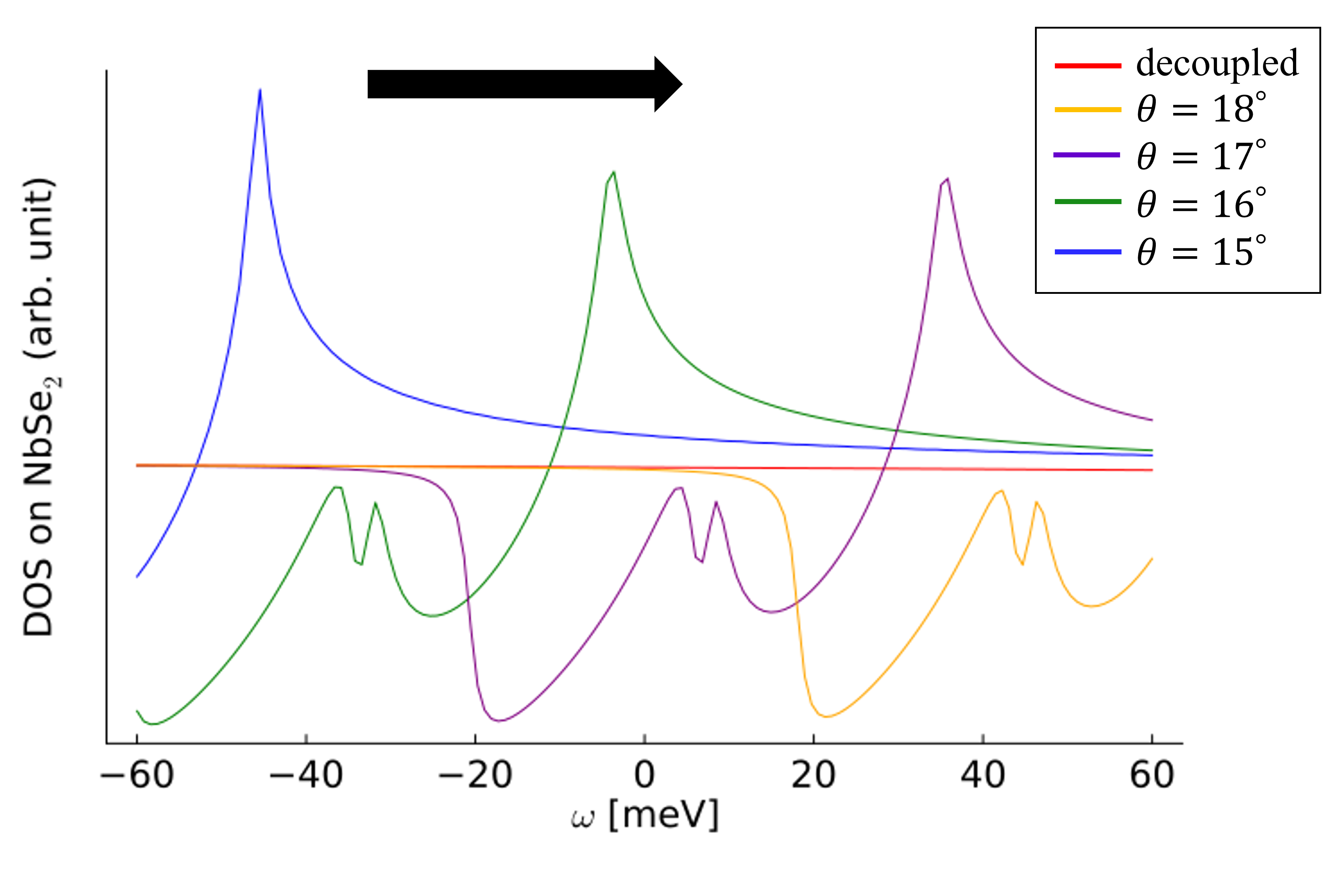
We first consider the Hamiltonian Eq. (24). This case is simple compared with the case of Eq. (20), where the presence of two order parameters and makes the relationship between the DOS and SC gaps complicated. Figure 10 shows the DOS near the Fermi level calculated from Eqs. (24) and (54), in comparison with the decoupled system, i.e., meV.
From Fig. 10, we notice that the DOS is larger than that of the decoupled system in a certain energy region. This region is located adjacent to the region where the DOS is suppressed by hybridization with graphene as mentioned in the previous subsection. As the twist angle increases, the energy dependence of the DOS shifts almost parallel to the higher energy side due to the shift of momentum that suffers the interlayer band hybridization. This behavior of the normal DOS on the NbSe2 layer is expected to modulate the SC state nonmonotonically. In particular, the substantial enhancement of the DOS near the Fermi level results in a sharp rise of the SC order parameter for . In contrast, as the twist angle is subsequently increased, the SC order parameter is decreased by a steep decrease of the DOS at the Fermi level (Fig. 10). This predicted behavior agrees well with the result of Fig. 5. These results suggest that we can control suppression and enhancement of the SC state by modifying the normal DOS through graphene substrates.
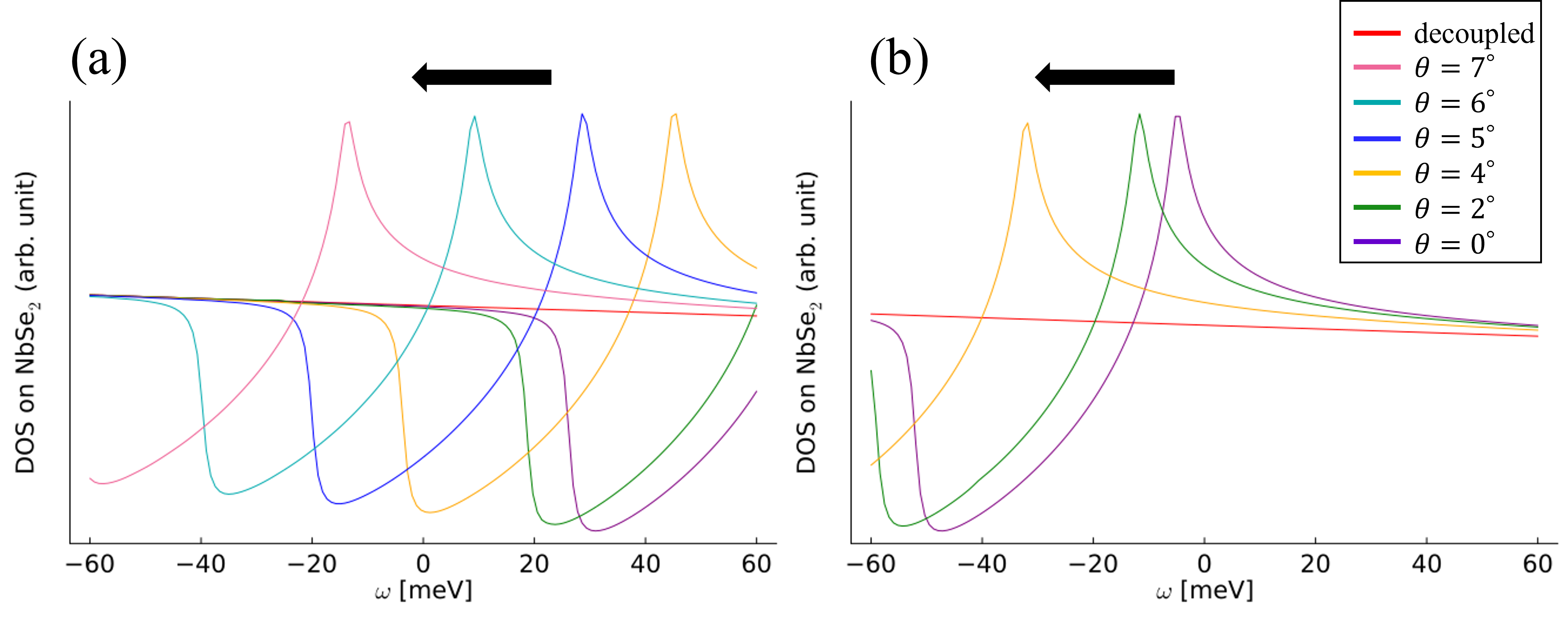
We next consider the Hamiltonian for the K valleys Eq. (20). The gap function is related to the spin up band, while is related to the spin down band in our definition. Since , we show and in Figs. 11(a) and 11(b), respectively. Similarly to the case of Eq. (24) and Fig. 10, we see the energy regions where the DOS is suppressed or enhanced by band hybridization. On the other hand, in contrast to Fig. 10, the DOS shifts to the lower energy side as the twist angle increases. This dissimilarity stems from the contrasting motion of graphene FSs in the Brillouin zone of NbSe2 with tuning the twist angle. Near , the graphene FSs move away from the NbSe2 FSs around the K valley as increases. In contrast, increasing the twist angle around makes the graphene FSs closer to the NbSe2 FSs around the point. These behaviors result in the qualitatively different twist angle dependence of the DOS. Analysis of the DOS is consistent with the twist angle dependence of the SC gap functions in Fig. 5. In Fig.11(a), the DOS at the Fermi level is most significantly suppressed near , where the SC gap function shows the minimum. In contrast, Fig. 11(b) reveals that the region with decreased can never encompass the Fermi level for arbitrary twist angles. This indicates that the gap function of the inner FS never becomes smaller than the decoupled case, and this is indeed seen in Fig. 5. The contrasting behavior of the gap functions and comes from the non-equivalence between the up and down spins originating from the Ising SOC. The non-equivalence is usually small because the SOC is smaller than the Fermi energy. However, in the twisted bilayer, the graphene’s electrons selectively hybridize with the up spin electrons around the K valley of NbSe2, which amplifies the difference of and and accordingly the non-equivalence of and . In other words, the effects of the Ising SOC, such as the parity mixing in Cooper pairs, can be enhanced by the twisted heterostructures.
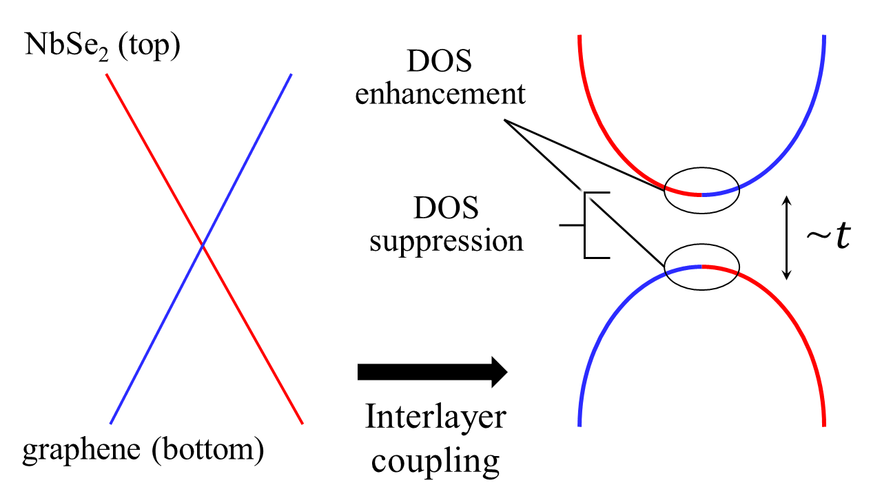
To conclude this section, we consider the cause of the characteristic shape of the DOS. In all the cases, the normal DOS shows the common feature that the energy region with enhanced DOS is adjacent to one with suppressed DOS. We show a schematic image in Fig. 12 depicting the relationship between the band hybridization and the normal DOS. The red and blue lines symbolically represent the energy band of the NbSe2 and graphene layers. In the presence of the interlayer coupling, a minigap opens at the band crossing point. This leads to the formation of an empty region, which corresponds to the energy region with suppressed DOS in Figs. 10 and 11. In conjunction with this minigap formation, the saddle points at the edge of the energy bands create van Hove singularities Moon and Koshino (2013); Brihuega et al. (2012); Havener et al. (2014); Jones et al. (2020). These van Hove singularities enhance the normal DOS, leading to the peaks in the DOS that we see in Figs. 10 and 11. The van Hove singularities are inevitably adjacent to the band gap, and therefore, the energy region with the suppressed normal DOS and that with the enhanced DOS appear adjacent. When we vary the twist angle, the position of the band-crossing point shifts to either a higher or lower energy side. This shift is the cause of the parallel shift of the normal DOS.
III.3 Low-energy Bogoliubov quasiparticles on NbSe2
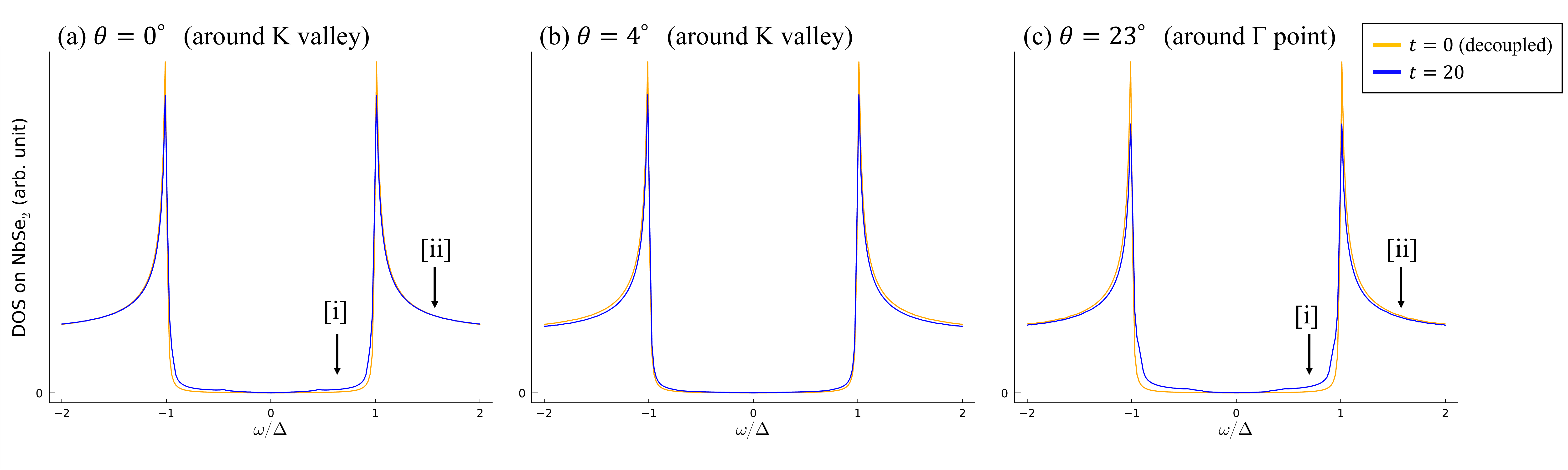
To obtain further insights into the SC states in twisted heterostructures, we here investigate the properties of Bogoliubov quasiparticles. We have assumed simple momentum-independent s-wave gap functions. However, the SC gap of Bogoliubov quasiparticles is not uniform in the momentum space. To study the SC gap in detail, we calculate the spectral function and the DOS in the SC state. In this section, we intentionally set meV and diagonalize the BdG Hamiltonian Eqs. (36) and (39).
Similarly to the normal state, the spectral function and the DOS contributed from the superconducting NbSe2 layer are given by
| (55) | ||||
| (56) |
where we represent the total amplitudes of the NbSe2 layer by and () in Eq. (43), and we now consider the physical quantities by summing for spin . Note that is the partial DOS on the NbSe2 layer and not the total DOS including the graphene states, which were studied in Ref. Gani et al., 2019. The scanning tunneling spectroscopy from the top NbSe2 layer measures the partial DOS rather than the total DOS.
Figure 13 shows the results of calculated by for and by for in comparison with the decoupled system. We notice that the DOS in the SC states is modified by the graphene substrate. In particular, the DOS inside the coherence peaks is larger than the decoupled system due to the interlayer band hybridization, which is especially noticeable in Figs. 13(a) and 13(c). This result exemplifies that the low-energy Bogoliubov quasiparticles emerge on the NbSe2 layer by the interlayer coupling.
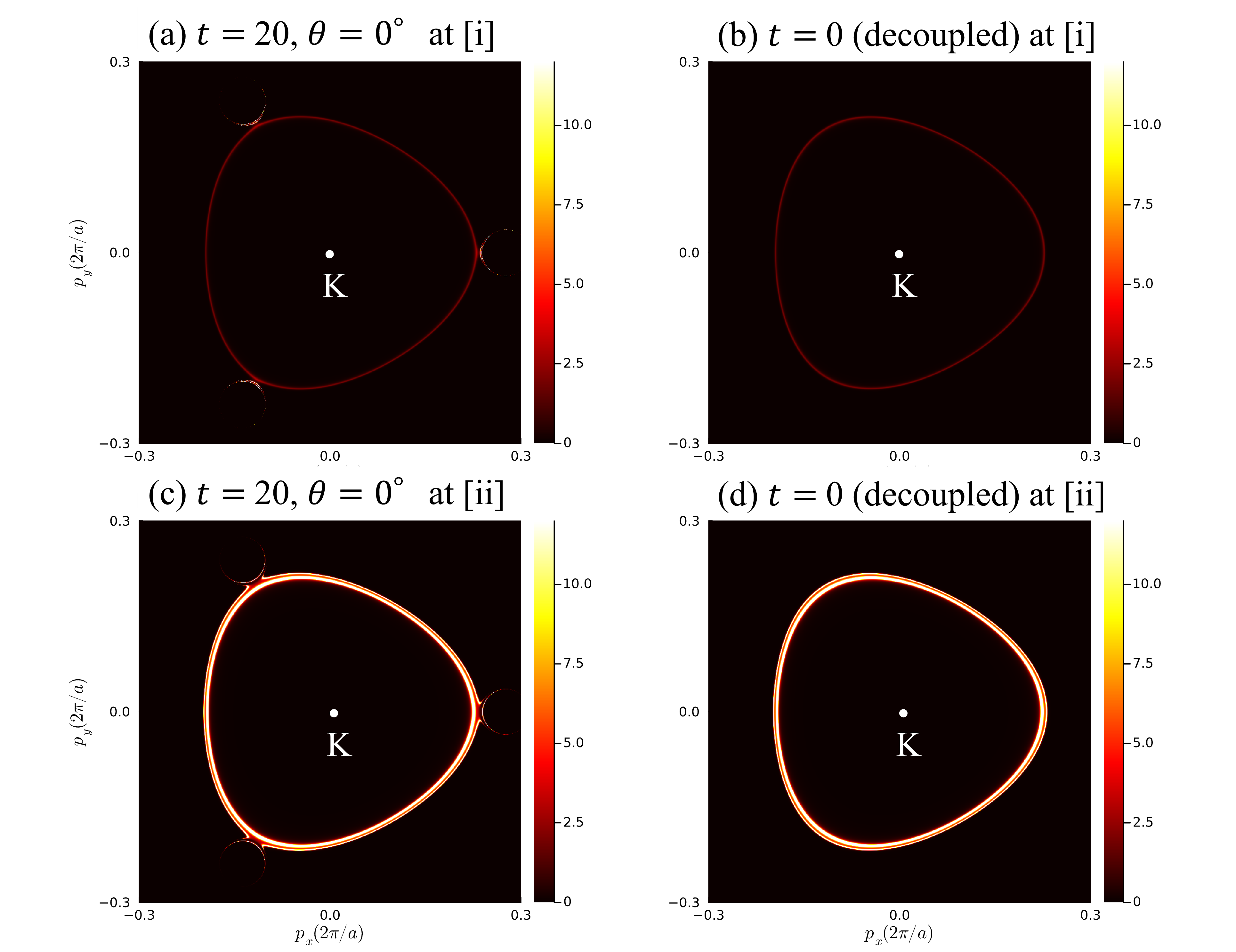
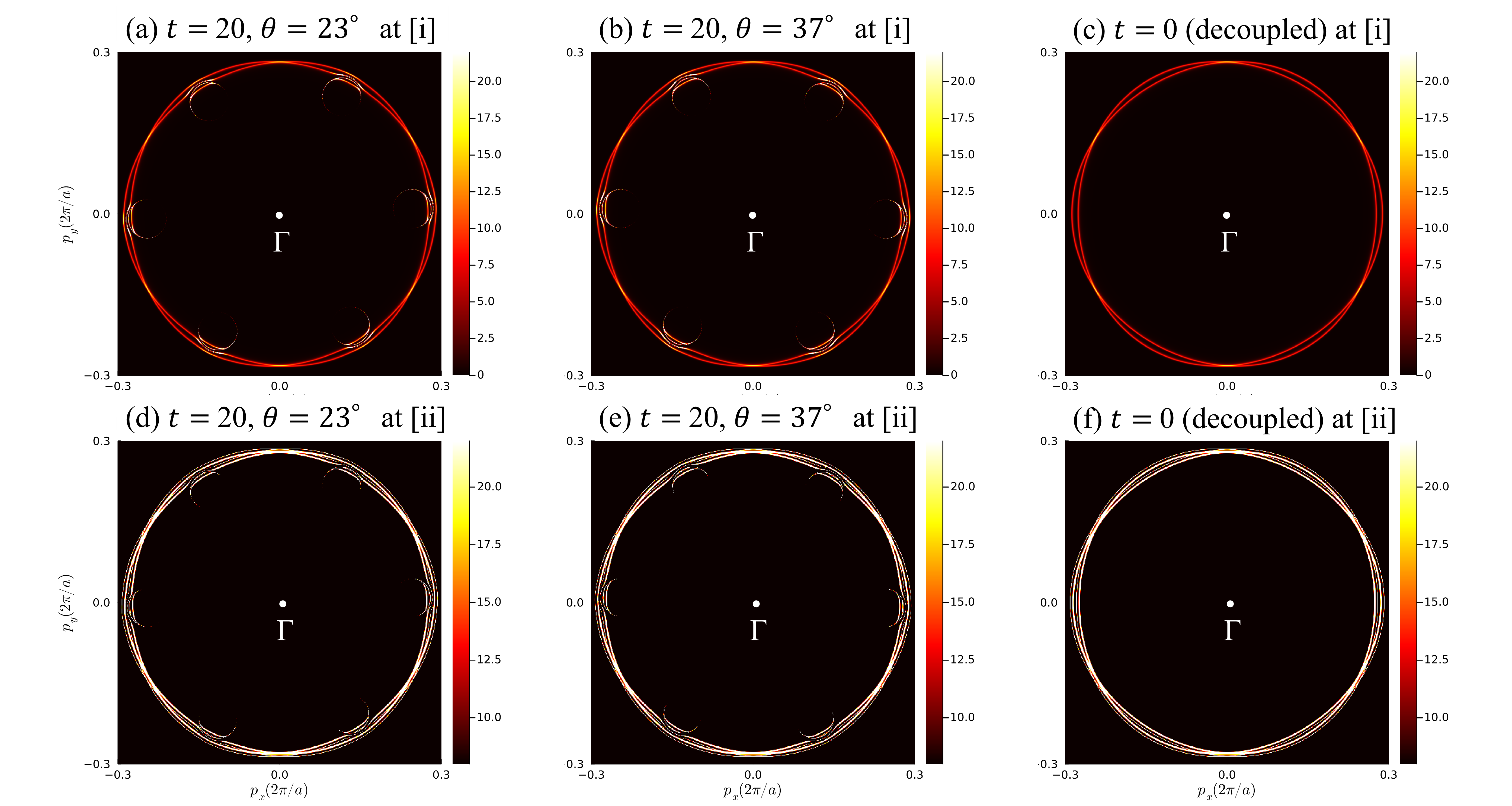
To clarify the characteristics of the low-energy quasiparticles, we show the calculated spectral function around the K valley and the point in Figs. 14 and 15. In these figures, we set [i] or [ii] where or . We also show the spectral function in the decoupled system. A common feature is that the bright white lines originating from the NbSe2 energy band are visible outside the coherence peaks in Figs. 14(c),(d) and 15(d)-(f). On the other hand, they are only faintly visible inside the coherence peaks due to the broadening, as represented by the red lines in Figs. 14(a),(b) and 15(a)-(c). However, in the twisted NbSe2 graphene heterostructures, the high-intensity spots appear near the crossing points of the NbSe2 and graphene energy bands. This means that the low-energy Bogoliubov quasiparticles emerge on the NbSe2 layer through band hybridization. Indeed, these low-energy states disappear in the absence of the interlayer coupling, i.e., in the monolayer NbSe2 [see Figs. 14(b) and 15(c)].
It is worth mentioning that except for and , the spectral functions break the in-plane mirror symmetry, which reflect the mirror symmetry breaking in real space. In other words, the twisted bilayer with twist angle and that with are mirror images of each other Zhu and Yakobson (2024). Moreover, the twisted bilayer with is equivalent to the one with due to the symmetry in reciprocal space. In fact, the spectral function for shown in Figs. 15(b) and 15(e) are the mirror reflection of Figs. 15(a) and 15(d), respectively. The in-plane mirror symmetry breaking by twisting combined with the out-of-plane mirror symmetry breaking by the heterostructure realizes a chiral crystalline structure in the real space. Accordingly, our results have verified the Bogoliubov quasiparticles with a chiral structure in momentum space.
IV Conclusion
In this paper, we have shown that a combination of a structure and metallic substrate effects tunes the monolayer superconductivity drastically. In particular, the twisted NbSe2 graphene heterostructure has been considered, assuming the situation of a monolayer NbSe2 stacked with a twist on a doped graphene substrate. By considering the generalized Umklapp process, we have developed a model applicable to a wider range of systems than the previous study. Our analysis of the model elucidated the SC states in detail.
In the numerical calculation, we revealed that the SC states on the NbSe2 layer, i.e., the order parameters are modified by varying the twist angle. The order parameters are strongly suppressed when the FSs of NbSe2 and graphene layers maximally overlap. This result indicates that the modulation of the SC states originates from the interlayer band hybridization between a monolayer superconductor and a monolayer normal metal. Furthermore, we uncovered that superconductivity can also be enhanced by slightly changing the twist angle. The interlayer band hybridization creates a region where the DOS on the NbSe2 layer is increased. As a result, the SC gap and the transition temperature increase when the enlarged DOS is located at the Fermi level. We also showed that the interlayer hybridization selectively enhances or suppresses the SC gap on the spin-split K valleys of NbSe2 due to the Ising SOC and effectively induces significant parity mixing in Cooper pairs.
We next studied the SC quasiparticles in detail. The low-energy Bogoliubov quasiparticles originating from the graphene layer have been found to emerge on the NbSe2 layer. That is, through the interlayer coupling the electronic structures seep out of the bottom graphene layer on the top NbSe2 layer. These low-energy quasiparticles reflect the in-plane mirror symmetry breaking, consistent with the recent observation of chiral Bogoliubov quasiparticles in the twisted NbSe2 graphene heterostructure Nar .
Our results support the usefulness of designing monolayer superconductivity by twist and substrate effects. This perspective unveils a way to realize unconventional superconductivity and explore the application of functional superconductors. Moreover, our model can be extended to study other TMDs, other material groups, and even cases where the crystal structure of each layer is different. It is expected to be fruitful in exploring a wide range of systems in future work.
acknowledgement
We appreciate Masahiro Naritsuka, Tadashi Machida, and Tetsuo Hanaguri for fruitful discussions from an experimental viewpoint. We also thank fruitful discussions with Michiya Chazono, Ryotaro Sano, Shin Kaneshiro, Hiroto Tanaka, and Koki Shinada. This work was supported by JSPS KAKENHI (Grant Nos. JP21K18145, JP22H01181, JP22H04933, JP23K22452, JP23K17353, JP24H00007).
References
- Saito et al. (2016a) Yu Saito, Tsutomu Nojima, and Yoshihiro Iwasa, “Highly crystalline 2d superconductors,” Nature Reviews Materials 2, 16094 (2016a).
- Brun et al. (2016) Christophe Brun, Tristan Cren, and Dimitri Roditchev, “Review of 2d superconductivity: the ultimate case of epitaxial monolayers,” Superconductor Science and Technology 30, 013003 (2016).
- Qiu et al. (2021) Dong Qiu, Chuanhui Gong, SiShuang Wang, Miao Zhang, Chao Yang, Xianfu Wang, and Jie Xiong, “Recent advances in 2d superconductors,” Advanced Materials 33, 2006124 (2021).
- Ohtomo and Hwang (2004) A. Ohtomo and H. Y. Hwang, “A high-mobility electron gas at the heterointerface,” Nature 427, 423–426 (2004).
- Gupta et al. (2015) Ankur Gupta, Tamilselvan Sakthivel, and Sudipta Seal, “Recent development in 2d materials beyond graphene,” Progress in Materials Science 73, 44–126 (2015).
- Gariglio et al. (2015) S. Gariglio, M. Gabay, J. Mannhart, and J.-M. Triscone, “Interface superconductivity,” Physica C: Superconductivity and its Applications 514, 189–198 (2015).
- Wang et al. (2016) Lili Wang, Xucun Ma, and Qi-Kun Xue, “Interface high-temperature superconductivity,” Superconductor Science and Technology 29, 123001 (2016).
- Tan et al. (2013) Shiyong Tan, Yan Zhang, Miao Xia, Zirong Ye, Fei Chen, Xin Xie, Rui Peng, Difei Xu, Qin Fan, Haichao Xu, Juan Jiang, Tong Zhang, Xinchun Lai, Tao Xiang, Jiangping Hu, Binping Xie, and Donglai Feng, “Interface-induced superconductivity and strain-dependent spin density waves in thin films,” Nature Materials 12, 634–640 (2013).
- Liu et al. (2012) Defa Liu, Wenhao Zhang, Daixiang Mou, Junfeng He, Yun-Bo Ou, Qing-Yan Wang, Zhi Li, Lili Wang, Lin Zhao, Shaolong He, Yingying Peng, Xu Liu, Chaoyu Chen, Li Yu, Guodong Liu, Xiaoli Dong, Jun Zhang, Chuangtian Chen, Zuyan Xu, Jiangping Hu, Xi Chen, Xucun Ma, Qikun Xue, and X. J. Zhou, “Electronic origin of high-temperature superconductivity in single-layer fese superconductor,” Nature Communications 3, 931 (2012).
- He et al. (2013) Shaolong He, Junfeng He, Wenhao Zhang, Lin Zhao, Defa Liu, Xu Liu, Daixiang Mou, Yun-Bo Ou, Qing-Yan Wang, Zhi Li, Lili Wang, Yingying Peng, Yan Liu, Chaoyu Chen, Li Yu, Guodong Liu, Xiaoli Dong, Jun Zhang, Chuangtian Chen, Zuyan Xu, Xi Chen, Xucun Ma, Qikun Xue, and X. J. Zhou, “Phase diagram and electronic indication of high-temperature superconductivity at 65 k in single-layer fese films,” Nature Materials 12, 605–610 (2013).
- Xiang et al. (2012) Yuan-Yuan Xiang, Fa Wang, Da Wang, Qiang-Hua Wang, and Dung-Hai Lee, “High-temperature superconductivity at the interface,” Phys. Rev. B 86, 134508 (2012).
- Mak et al. (2010) Kin Fai Mak, Changgu Lee, James Hone, Jie Shan, and Tony F. Heinz, “Atomically thin : A new direct-gap semiconductor,” Phys. Rev. Lett. 105, 136805 (2010).
- Ye et al. (2012) J. T. Ye, Y. J. Zhang, R. Akashi, M. S. Bahramy, R. Arita, and Y. Iwasa, “Superconducting dome in a gate-tuned band insulator,” Science 338, 1193–1196 (2012).
- Voiry et al. (2015) Damien Voiry, Aditya Mohite, and Manish Chhowalla, “Phase engineering of transition metal dichalcogenides,” Chem. Soc. Rev. 44, 2702–2712 (2015).
- Wang et al. (2012) Qing Hua Wang, Kourosh Kalantar-Zadeh, Andras Kis, Jonathan N. Coleman, and Michael S. Strano, “Electronics and optoelectronics of two-dimensional transition metal dichalcogenides,” Nature Nanotechnology 7, 699–712 (2012).
- Han et al. (2018) Gang Hee Han, Dinh Loc Duong, Dong Hoon Keum, Seok Joon Yun, and Young Hee Lee, “van der waals metallic transition metal dichalcogenides,” Chemical Reviews 118, 6297–6336 (2018).
- Devarakonda et al. (2020) A. Devarakonda, H. Inoue, S. Fang, C. Ozsoy-Keskinbora, T. Suzuki, M. Kriener, L. Fu, E. Kaxiras, D. C. Bell, and J. G. Checkelsky, “Clean 2d superconductivity in a bulk van der waals superlattice,” Science 370, 231–236 (2020).
- Ding et al. (2011) Yi Ding, Yanli Wang, Jun Ni, Lin Shi, Siqi Shi, and Weihua Tang, “First principles study of structural, vibrational and electronic properties of graphene-like () monolayers,” Physica B: Condensed Matter 406, 2254–2260 (2011).
- Xi et al. (2015) Xiaoxiang Xi, Liang Zhao, Zefang Wang, Helmuth Berger, László Forró, Jie Shan, and Kin Fai Mak, “Strongly enhanced charge-density-wave order in monolayer ,” Nature Nanotechnology 10, 765–769 (2015).
- Costanzo et al. (2016) Davide Costanzo, Sanghyun Jo, Helmuth Berger, and Alberto F. Morpurgo, “Gate-induced superconductivity in atomically thin crystals,” Nature Nanotechnology 11, 339–344 (2016).
- Saito et al. (2016b) Yu Saito, Yasuharu Nakamura, Mohammad Saeed Bahramy, Yoshimitsu Kohama, Jianting Ye, Yuichi Kasahara, Yuji Nakagawa, Masaru Onga, Masashi Tokunaga, Tsutomu Nojima, Youichi Yanase, and Yoshihiro Iwasa, “Superconductivity protected by spin–valley locking in ion-gated ,” Nature Physics 12, 144–149 (2016b).
- Navarro-Moratalla et al. (2016) Efrén Navarro-Moratalla, Joshua O. Island, Samuel Mañas-Valero, Elena Pinilla-Cienfuegos, Andres Castellanos-Gomez, Jorge Quereda, Gabino Rubio-Bollinger, Luca Chirolli, Jose Angel Silva-Guillén, Nicolás Agraït, Gary A. Steele, Francisco Guinea, Herre S. J. van der Zant, and Eugenio Coronado, “Enhanced superconductivity in atomically thin ,” Nature Communications 7, 11043 (2016).
- Peng et al. (2018) Jing Peng, Zhi Yu, Jiajing Wu, Yuan Zhou, Yuqiao Guo, Zejun Li, Jiyin Zhao, Changzheng Wu, and Yi Xie, “Disorder enhanced superconductivity toward monolayer,” ACS Nano 12, 9461–9466 (2018).
- Yokoya et al. (2001) T Yokoya, T Kiss, A Chainani, S Shin, M Nohara, and H Takagi, “Fermi surface sheet-dependent superconductivity in ,” Science 294, 2518–2520 (2001).
- Khestanova et al. (2018) E. Khestanova, J. Birkbeck, M. Zhu, Y. Cao, G. L. Yu, D. Ghazaryan, J. Yin, H. Berger, L. Forró, T. Taniguchi, K. Watanabe, R. V. Gorbachev, A. Mishchenko, A. K. Geim, and I. V. Grigorieva, “Unusual suppression of the superconducting energy gap and critical temperature in atomically thin ,” Nano Letters 18, 2623–2629 (2018).
- Dvir et al. (2018) T. Dvir, F. Massee, L. Attias, M. Khodas, M. Aprili, C. H. L. Quay, and H. Steinberg, “Spectroscopy of bulk and few-layer superconducting with van der waals tunnel junctions,” Nature Communications 9, 598 (2018).
- Wickramaratne et al. (2020) Darshana Wickramaratne, Sergii Khmelevskyi, Daniel F. Agterberg, and I. I. Mazin, “Ising superconductivity and magnetism in ,” Phys. Rev. X 10, 041003 (2020).
- Noat et al. (2015) Y. Noat, J. A. Silva-Guillén, T. Cren, V. Cherkez, C. Brun, S. Pons, F. Debontridder, D. Roditchev, W. Sacks, L. Cario, P. Ordejón, A. García, and E. Canadell, “Quasiparticle spectra of : Two-band superconductivity and the role of tunneling selectivity,” Phys. Rev. B 92, 134510 (2015).
- Zheng and Feng (2019) Feipeng Zheng and Ji Feng, “Electron-phonon coupling and the coexistence of superconductivity and charge-density wave in monolayer ,” Phys. Rev. B 99, 161119 (2019).
- Xi et al. (2016) Xiaoxiang Xi, Zefang Wang, Weiwei Zhao, Ju-Hyun Park, Kam Tuen Law, Helmuth Berger, László Forró, Jie Shan, and Kin Fai Mak, “Ising pairing in superconducting atomic layers,” Nature Physics 12, 139–143 (2016).
- Lu et al. (2015) J. M. Lu, O. Zheliuk, I. Leermakers, N. F. Q. Yuan, U. Zeitler, K. T. Law, and J. T. Ye, “Evidence for two-dimensional ising superconductivity in gated ,” Science 350, 1353–1357 (2015).
- Wang et al. (2017) Hong Wang, Xiangwei Huang, Junhao Lin, Jian Cui, Yu Chen, Chao Zhu, Fucai Liu, Qingsheng Zeng, Jiadong Zhou, Peng Yu, Xuewen Wang, Haiyong He, Siu Hon Tsang, Weibo Gao, Kazu Suenaga, Fengcai Ma, Changli Yang, Li Lu, Ting Yu, Edwin Hang Tong Teo, Guangtong Liu, and Zheng Liu, “High-quality monolayer superconductor grown by chemical vapour deposition,” Nature Communications 8, 394 (2017).
- Ugeda et al. (2016) Miguel M. Ugeda, Aaron J. Bradley, Yi Zhang, Seita Onishi, Yi Chen, Wei Ruan, Claudia Ojeda-Aristizabal, Hyejin Ryu, Mark T. Edmonds, Hsin-Zon Tsai, Alexander Riss, Sung-Kwan Mo, Dunghai Lee, Alex Zettl, Zahid Hussain, Zhi-Xun Shen, and Michael F. Crommie, “Characterization of collective ground states in single-layer ,” Nature Physics 12, 92–97 (2016).
- de la Barrera et al. (2018) Sergio C. de la Barrera, Michael R. Sinko, Devashish P. Gopalan, Nikhil Sivadas, Kyle L. Seyler, Kenji Watanabe, Takashi Taniguchi, Adam W. Tsen, Xiaodong Xu, Di Xiao, and Benjamin M. Hunt, “Tuning ising superconductivity with layer and spin–orbit coupling in two-dimensional transition-metal dichalcogenides,” Nature Communications 9, 1427 (2018).
- Xing et al. (2017) Ying Xing, Kun Zhao, Pujia Shan, Feipeng Zheng, Yangwei Zhang, Hailong Fu, Yi Liu, Mingliang Tian, Chuanying Xi, Haiwen Liu, Ji Feng, Xi Lin, Shuaihua Ji, Xi Chen, Qi-Kun Xue, and Jian Wang, “Ising superconductivity and quantum phase transition in macro-size monolayer ,” Nano Letters 17, 6802–6807 (2017).
- Wan et al. (2022) Wen Wan, Paul Dreher, Daniel Muñoz-Segovia, Rishav Harsh, Haojie Guo, Antonio J. Martínez-Galera, Francisco Guinea, Fernando de Juan, and Miguel M. Ugeda, “Observation of superconducting collective modes from competing pairing instabilities in single-layer ,” Advanced Materials 34, 2206078 (2022).
- Naritsuka et al. (2021) M Naritsuka, T Terashima, and Y Matsuda, “Controlling unconventional superconductivity in artificially engineered f-electron kondo superlattices,” Journal of Physics: Condensed Matter 33, 273001 (2021).
- Goh et al. (2012) S. K. Goh, Y. Mizukami, H. Shishido, D. Watanabe, S. Yasumoto, M. Shimozawa, M. Yamashita, T. Terashima, Y. Yanase, T. Shibauchi, A. I. Buzdin, and Y. Matsuda, “Anomalous upper critical field in superlattices with a rashba-type heavy fermion interface,” Phys. Rev. Lett. 109, 157006 (2012).
- Shishido et al. (2010) H. Shishido, T. Shibauchi, K. Yasu, T. Kato, H. Kontani, T. Terashima, and Y. Matsuda, “Tuning the dimensionality of the heavy fermion compound ,” Science 327, 980–983 (2010).
- Mizukami et al. (2011) Y. Mizukami, H. Shishido, T. Shibauchi, M. Shimozawa, S. Yasumoto, D. Watanabe, M. Yamashita, H. Ikeda, T. Terashima, H. Kontani, and Y. Matsuda, “Extremely strong-coupling superconductivity in artificial two-dimensional kondo lattices,” Nature Physics 7, 849–853 (2011).
- Niu and Li (2015) Tianchao Niu and Ang Li, “From two-dimensional materials to heterostructures,” Progress in Surface Science 90, 21–45 (2015), special Issue on Silicene.
- Kim et al. (2016) Kyounghwan Kim, Matthew Yankowitz, Babak Fallahazad, Sangwoo Kang, Hema C. P. Movva, Shengqiang Huang, Stefano Larentis, Chris M. Corbet, Takashi Taniguchi, Kenji Watanabe, Sanjay K. Banerjee, Brian J. LeRoy, and Emanuel Tutuc, “Van der waals heterostructures with high accuracy rotational alignment,” Nano Letters 16, 1989–1995 (2016).
- Veneri et al. (2022) Alessandro Veneri, David T. S. Perkins, Csaba G. Péterfalvi, and Aires Ferreira, “Twist angle controlled collinear edelstein effect in van der waals heterostructures,” Phys. Rev. B 106, L081406 (2022).
- Nie et al. (2023) Jin-Hua Nie, Tao Xie, Gang Chen, Wenhao Zhang, and Ying-Shuang Fu, “Moiré enhanced two-band superconductivity in a heterojunction,” Nano Letters 23, 8370–8377 (2023).
- Li and Koshino (2019) Yang Li and Mikito Koshino, “Twist-angle dependence of the proximity spin-orbit coupling in graphene on transition-metal dichalcogenides,” Phys. Rev. B 99, 075438 (2019).
- Xiao et al. (2023) Jiewen Xiao, Yaar Vituri, and Erez Berg, “Probing the order parameter symmetry of two-dimensional superconductors by twisted josephson interferometry,” Phys. Rev. B 108, 094520 (2023).
- Dreher et al. (2021) Paul Dreher, Wen Wan, Alla Chikina, Marco Bianchi, Haojie Guo, Rishav Harsh, Samuel Mañas-Valero, Eugenio Coronado, Antonio J. Martínez-Galera, Philip Hofmann, Jill A. Miwa, and Miguel M. Ugeda, “Proximity effects on the charge density wave order and superconductivity in single-layer ,” ACS Nano 15, 19430–19438 (2021).
- Geim and Grigorieva (2013) A. K. Geim and I. V. Grigorieva, “Van der waals heterostructures,” Nature 499, 419–425 (2013).
- Kennes et al. (2021) Dante M. Kennes, Martin Claassen, Lede Xian, Antoine Georges, Andrew J. Millis, James Hone, Cory R. Dean, D. N. Basov, Abhay N. Pasupathy, and Angel Rubio, “Moiré heterostructures as a condensed-matter quantum simulator,” Nature Physics 17, 155–163 (2021).
- Behura et al. (2021) Sanjay K. Behura, Alexis Miranda, Sasmita Nayak, Kayleigh Johnson, Priyanka Das, and Nihar R. Pradhan, “Moiré physics in twisted van der waals heterostructures of 2d materials,” Emergent Materials 4, 813–826 (2021).
- Liao et al. (2019) Wugang Liao, Yanting Huang, Huide Wang, and Han Zhang, “Van der waals heterostructures for optoelectronics: Progress and prospects,” Applied Materials Today 16, 435–455 (2019).
- Tran et al. (2020) Kha Tran, Junho Choi, and Akshay Singh, “Moiré and beyond in transition metal dichalcogenide twisted bilayers,” 2D Materials 8, 022002 (2020).
- Cao et al. (2018a) Yuan Cao, Valla Fatemi, Shiang Fang, Kenji Watanabe, Takashi Taniguchi, Efthimios Kaxiras, and Pablo Jarillo-Herrero, “Unconventional superconductivity in magic-angle graphene superlattices,” Nature 556, 43–50 (2018a).
- Cao et al. (2018b) Yuan Cao, Valla Fatemi, Ahmet Demir, Shiang Fang, Spencer L. Tomarken, Jason Y. Luo, Javier D. Sanchez-Yamagishi, Kenji Watanabe, Takashi Taniguchi, Efthimios Kaxiras, Ray C. Ashoori, and Pablo Jarillo-Herrero, “Correlated insulator behaviour at half-filling in magic-angle graphene superlattices,” Nature 556, 80–84 (2018b).
- Yankowitz et al. (2019) Matthew Yankowitz, Shaowen Chen, Hryhoriy Polshyn, Yuxuan Zhang, K. Watanabe, T. Taniguchi, David Graf, Andrea F. Young, and Cory R. Dean, “Tuning superconductivity in twisted bilayer graphene,” Science 363, 1059–1064 (2019).
- Tarnopolsky et al. (2019) Grigory Tarnopolsky, Alex Jura Kruchkov, and Ashvin Vishwanath, “Origin of magic angles in twisted bilayer graphene,” Phys. Rev. Lett. 122, 106405 (2019).
- Andrei and MacDonald (2020) Eva Y. Andrei and Allan H. MacDonald, “Graphene bilayers with a twist,” Nature Materials 19, 1265–1275 (2020).
- Ramires and Lado (2018) Aline Ramires and Jose L. Lado, “Electrically tunable gauge fields in tiny-angle twisted bilayer graphene,” Phys. Rev. Lett. 121, 146801 (2018).
- Qin and MacDonald (2021) Wei Qin and Allan H. MacDonald, “In-plane critical magnetic fields in magic-angle twisted trilayer graphene,” Phys. Rev. Lett. 127, 097001 (2021).
- Ray et al. (2019) Sujay Ray, Jeil Jung, and Tanmoy Das, “Wannier pairs in superconducting twisted bilayer graphene and related systems,” Phys. Rev. B 99, 134515 (2019).
- Scheurer and Samajdar (2020) Mathias S. Scheurer and Rhine Samajdar, “Pairing in graphene-based moiré superlattices,” Phys. Rev. Res. 2, 033062 (2020).
- Peltonen et al. (2018) Teemu J. Peltonen, Risto Ojajärvi, and Tero T. Heikkilä, “Mean-field theory for superconductivity in twisted bilayer graphene,” Phys. Rev. B 98, 220504 (2018).
- Christos et al. (2023) Maine Christos, Subir Sachdev, and Mathias S. Scheurer, “Nodal band-off-diagonal superconductivity in twisted graphene superlattices,” Nature Communications 14, 7134 (2023).
- Oh et al. (2021) Myungchul Oh, Kevin P. Nuckolls, Dillon Wong, Ryan L. Lee, Xiaomeng Liu, Kenji Watanabe, Takashi Taniguchi, and Ali Yazdani, “Evidence for unconventional superconductivity in twisted bilayer graphene,” Nature 600, 240–245 (2021).
- Wu et al. (2018) Fengcheng Wu, A. H. MacDonald, and Ivar Martin, “Theory of phonon-mediated superconductivity in twisted bilayer graphene,” Phys. Rev. Lett. 121, 257001 (2018).
- Po et al. (2018) Hoi Chun Po, Liujun Zou, Ashvin Vishwanath, and T. Senthil, “Origin of mott insulating behavior and superconductivity in twisted bilayer graphene,” Phys. Rev. X 8, 031089 (2018).
- Isobe et al. (2018) Hiroki Isobe, Noah F. Q. Yuan, and Liang Fu, “Unconventional superconductivity and density waves in twisted bilayer graphene,” Phys. Rev. X 8, 041041 (2018).
- Saito et al. (2020) Yu Saito, Jingyuan Ge, Kenji Watanabe, Takashi Taniguchi, and Andrea F. Young, “Independent superconductors and correlated insulators in twisted bilayer graphene,” Nature Physics 16, 926–930 (2020).
- Arora et al. (2020) Harpreet Singh Arora, Robert Polski, Yiran Zhang, Alex Thomson, Youngjoon Choi, Hyunjin Kim, Zhong Lin, Ilham Zaky Wilson, Xiaodong Xu, Jiun-Haw Chu, Kenji Watanabe, Takashi Taniguchi, Jason Alicea, and Stevan Nadj-Perge, “Superconductivity in metallic twisted bilayer graphene stabilized by ,” Nature 583, 379–384 (2020).
- González and Stauber (2019) J. González and T. Stauber, “Kohn-luttinger superconductivity in twisted bilayer graphene,” Phys. Rev. Lett. 122, 026801 (2019).
- Codecido et al. (2019) Emilio Codecido, Qiyue Wang, Ryan Koester, Shi Che, Haidong Tian, Rui Lv, Son Tran, Kenji Watanabe, Takashi Taniguchi, Fan Zhang, Marc Bockrath, and Chun Ning Lau, “Correlated insulating and superconducting states in twisted bilayer graphene below the magic angle,” Science Advances 5, eaaw9770 (2019).
- Kerelsky et al. (2019) Alexander Kerelsky, Leo J. McGilly, Dante M. Kennes, Lede Xian, Matthew Yankowitz, Shaowen Chen, K. Watanabe, T. Taniguchi, James Hone, Cory Dean, Angel Rubio, and Abhay N. Pasupathy, “Maximized electron interactions at the magic angle in twisted bilayer graphene,” Nature 572, 95–100 (2019).
- Lisi et al. (2021) Simone Lisi, Xiaobo Lu, Tjerk Benschop, Tobias A. de Jong, Petr Stepanov, Jose R. Duran, Florian Margot, Irène Cucchi, Edoardo Cappelli, Andrew Hunter, Anna Tamai, Viktor Kandyba, Alessio Giampietri, Alexei Barinov, Johannes Jobst, Vincent Stalman, Maarten Leeuwenhoek, Kenji Watanabe, Takashi Taniguchi, Louk Rademaker, Sense Jan van der Molen, Milan P. Allan, Dmitri K. Efetov, and Felix Baumberger, “Observation of flat bands in twisted bilayer graphene,” Nature Physics 17, 189–193 (2021).
- Suárez Morell et al. (2010) E. Suárez Morell, J. D. Correa, P. Vargas, M. Pacheco, and Z. Barticevic, “Flat bands in slightly twisted bilayer graphene: Tight-binding calculations,” Phys. Rev. B 82, 121407 (2010).
- Zhang et al. (2020) Zhiming Zhang, Yimeng Wang, Kenji Watanabe, Takashi Taniguchi, Keiji Ueno, Emanuel Tutuc, and Brian J. LeRoy, “Flat bands in twisted bilayer transition metal dichalcogenides,” Nature Physics 16, 1093–1096 (2020).
- Devakul et al. (2021) Trithep Devakul, Valentin Crépel, Yang Zhang, and Liang Fu, “Magic in twisted transition metal dichalcogenide bilayers,” Nature Communications 12, 6730 (2021).
- Xian et al. (2021) Lede Xian, Ammon Fischer, Martin Claassen, Jin Zhang, Angel Rubio, and Dante M. Kennes, “Engineering three-dimensional moiré flat bands,” Nano Letters 21, 7519–7526 (2021).
- Zhang et al. (2018) Peng Zhang, Koichiro Yaji, Takahiro Hashimoto, Yuichi Ota, Takeshi Kondo, Kozo Okazaki, Zhijun Wang, Jinsheng Wen, G. D. Gu, Hong Ding, and Shik Shin, “Observation of topological superconductivity on the surface of an iron-based superconductor,” Science 360, 182–186 (2018).
- Machida et al. (2019) T. Machida, Y. Sun, S. Pyon, S. Takeda, Y. Kohsaka, T. Hanaguri, T. Sasagawa, and T. Tamegai, “Zero-energy vortex bound state in the superconducting topological surface state of ,” Nature Materials 18, 811–815 (2019).
- He et al. (2018) Wen-Yu He, Benjamin T. Zhou, James J. He, Noah F. Q. Yuan, Ting Zhang, and K. T. Law, “Magnetic field driven nodal topological superconductivity in monolayer transition metal dichalcogenides,” Communications Physics 1, 40 (2018).
- Kezilebieke et al. (2020) Shawulienu Kezilebieke, Md Nurul Huda, Viliam Vaňo, Markus Aapro, Somesh C. Ganguli, Orlando J. Silveira, Szczepan Głodzik, Adam S. Foster, Teemu Ojanen, and Peter Liljeroth, “Topological superconductivity in a van der waals heterostructure,” Nature 588, 424–428 (2020).
- Xie and Law (2023) Ying-Ming Xie and K. T. Law, “Orbital fulde-ferrell pairing state in moiré ising superconductors,” Phys. Rev. Lett. 131, 016001 (2023).
- Gani et al. (2019) Yohanes S. Gani, Hadar Steinberg, and Enrico Rossi, “Superconductivity in twisted graphene heterostructures,” Phys. Rev. B 99, 235404 (2019).
- Mele (2010) E. J. Mele, “Commensuration and interlayer coherence in twisted bilayer graphene,” Phys. Rev. B 81, 161405 (2010).
- Bistritzer and MacDonald (2011) Rafi Bistritzer and Allan H. MacDonald, “Moiré bands in twisted double-layer graphene,” Proceedings of the National Academy of Sciences 108, 12233–12237 (2011).
- Koshino and Nam (2020) Mikito Koshino and Nguyen N. T. Nam, “Effective continuum model for relaxed twisted bilayer graphene and moiré electron-phonon interaction,” Phys. Rev. B 101, 195425 (2020).
- Lopes dos Santos et al. (2007) J. M. B. Lopes dos Santos, N. M. R. Peres, and A. H. Castro Neto, “Graphene bilayer with a twist: Electronic structure,” Phys. Rev. Lett. 99, 256802 (2007).
- Koshino (2015) Mikito Koshino, “Interlayer interaction in general incommensurate atomic layers,” New Journal of Physics 17, 015014 (2015).
- David et al. (2019) Alessandro David, Péter Rakyta, Andor Kormányos, and Guido Burkard, “Induced spin-orbit coupling in twisted graphene–transition metal dichalcogenide heterobilayers: Twistronics meets spintronics,” Phys. Rev. B 100, 085412 (2019).
- Zhang et al. (2014) Junhua Zhang, C. Triola, and E. Rossi, “Proximity effect in graphene–topological-insulator heterostructures,” Phys. Rev. Lett. 112, 096802 (2014).
- Sticlet and Morari (2019) Doru Sticlet and Cristian Morari, “Topological superconductivity from magnetic impurities on monolayer ,” Phys. Rev. B 100, 075420 (2019).
- Bauer and Sigrist (2012) Ernst Bauer and Manfred Sigrist, “Non-centrosymmetric superconductors: introduction and overview,” (2012).
- Sato and Ando (2017) Masatoshi Sato and Yoichi Ando, “Topological superconductors: a review,” Reports on Progress in Physics 80, 076501 (2017).
- Eremenko et al. (2009) V. Eremenko, V. Sirenko, V. Ibulaev, J. Bartolomé, A. Arauzo, and G. Reményi, “Heat capacity, thermal expansion and pressure derivative of critical temperature at the superconducting and charge density wave (cdw) transitions in ,” Physica C: Superconductivity 469, 259–264 (2009).
- Moon and Koshino (2013) Pilkyung Moon and Mikito Koshino, “Optical absorption in twisted bilayer graphene,” Phys. Rev. B 87, 205404 (2013).
- Brihuega et al. (2012) I. Brihuega, P. Mallet, H. González-Herrero, G. Trambly de Laissardière, M. M. Ugeda, L. Magaud, J. M. Gómez-Rodríguez, F. Ynduráin, and J.-Y. Veuillen, “Unraveling the intrinsic and robust nature of van hove singularities in twisted bilayer graphene by scanning tunneling microscopy and theoretical analysis,” Phys. Rev. Lett. 109, 196802 (2012).
- Havener et al. (2014) Robin W. Havener, Yufeng Liang, Lola Brown, Li Yang, and Jiwoong Park, “Van hove singularities and excitonic effects in the optical conductivity of twisted bilayer graphene,” Nano Letters 14, 3353–3357 (2014).
- Jones et al. (2020) Alfred J. H. Jones, Ryan Muzzio, Paulina Majchrzak, Sahar Pakdel, Davide Curcio, Klara Volckaert, Deepnarayan Biswas, Jacob Gobbo, Simranjeet Singh, Jeremy T. Robinson, Kenji Watanabe, Takashi Taniguchi, Timur K. Kim, Cephise Cacho, Nicola Lanata, Jill A. Miwa, Philip Hofmann, Jyoti Katoch, and Søren Ulstrup, “Observation of electrically tunable van hove singularities in twisted bilayer graphene from nanoarpes,” Advanced Materials 32, 2001656 (2020).
- Zhu and Yakobson (2024) Hanyu Zhu and Boris I. Yakobson, “Creating chirality in the nearly two dimensions,” Nature Materials 23, 316–322 (2024).
- (100) Masahiro Naritsuka, Tadashi Machida, Shun Asano, Youichi Yanase, Tetsuo Hanaguri, submitted.