Institute of Physics, University of Oldenburg, 26129 Oldenburg, Germany
Inelastic electron-light scattering at dielectric thin films
Abstract
In a recently developed methodology termed photon induced near-field electron microscopy (PINEM), the inelastic scattering of electrons off illuminated nanostructures provides direct experimental access to the structure of optical near-field modes and their population. Whereas the inelastic scattering probability can be quantitatively linked to the near field distribution, analytical results for simple light scattering geometries are scarce. Here we derive a fully analytical expression for the coupling strength between free electrons and optical near-fields in planar geometries representing dielectric thin films. Contributions to the overall coupling from the electric field above, below and within the sample are analyzed in detail. By carefully choosing the relative angles between electron beam, light and thin film and by accounting for a broad spectrum of photon energies, we demonstrate that one can imprint optical material properties like the reflectivity onto the electron energy distribution.
keywords:
Ultrafast transmission electron microscopy, photon induced near-field electron microscopy, Fabry-Perot resonances, inelastic electron-light scattering1 Introduction
Electron microscopy is one of the most versatile tools for studying the structure and properties of materials on atomic length scales, addressing electronic, structural, and spin degrees of freedom 1. Recent instrumental and methodological developments have led to the invention of ultrafast transmission electron microscopy (UTEM). UTEM combines the unparalleled spatial resolution of electron microscopy with the high temporal resolution of ultrafast optics 2, 3, 4, 5 and allows for the observation of ultrafast structural dynamics and phase transitions 6, 7, 8, 9, 10 as well as magnetic dynamics 11, 12. More recently, a technique called photon-induced near-field electron microscopy (PINEM) has emerged as a promising tool for the imaging of optical near-fields in the vicinity of illuminated nano-structures 13, 14, 15, 16, 17. Examples include the spatio-temporally resolved imaging of polariton wave packets in 2D materials 18, the quantum coherent tailoring of the free electron wave function by light fields 19, 20, 21, 22, 23, 24, 25 and work towards free-electron/photon correlations in the few photon limit 26, 27, 28, 29. The fundamental mechanism governing PINEM consists of the temporal phase modulation of a free electron wave function within a localized electric field, which results in the inelastic electron scattering off the light field. The process can be interpreted as the stimulated emission or absorption of a photon into or from the near-field triggered by the passing electron and mediated by the broadened momentum spectrum of the near-field. In the past, the abrupt change in the electric field at planar material interfaces was used to imprint an optical phase modulation on an electron beam both in the longitudinal 19 and transverse 23 direction. An analytical expression for the electron-light coupling strength at a single reflective interface was given in Ref. 20, the more general case of inelastic electron scattering at an illuminated dielectric thin film was not considered analytically, yet.
Here, we introduce a fully analytical approach to calculate the interaction strength between a free electron and an optical near-field at a dielectric thin film. The thin film faces form a discontinuity in the spatial distribution of the transversal field component leading to a momentum broadening. We will show how the overall coupling is influenced by the partial fields before, inside and behind the thin film and how optical resonances can be mapped onto the electron photon coupling. Furthermore, we give an example how the resonances can be spectrally resolved using chirped light fields.
2 Description of the model
We consider a thin film of an optically isotropic material with a thickness and (complex) refractive index (Fig. 1(a,b)). As a specific example and without loss of generality, we have chosen silicon as the thin film material in all explicit calculations (dielectric function taken from 30, 31). A fast electron passes through the film with kinetic energy , e.g. keV at an angle .
Electric field - Fabry-Perot pattern
The material is illuminated with an external monochromatic plane-wave light field that constitutes the scattering obstacle for the incoming electron. The incoming light is characterized by an angular frequency , a wavevector (incident angle , see Fig. 1) and a transverse magnetic (TM) polarization. At both thin-film interfaces the incident light is partially reflected and transmitted, resulting in interference and the formation of a guided Fabry-Perot mode within the layer.
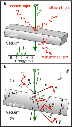
The resulting Fabry-Perot pattern is controlled by the parameters and , and on the incident angle of the light wave, .
Numerical simulation procedure
In each of the regions shown in Fig. 1 (above, inside and below the thin film) the electric field is a superposition of truncated plane waves with wavevectors corresponding to the transmitted and reflected wave components. The individual amplitudes of the plane waves in different regions are linked by the required continuity of the in-plane electric field components (i.e. ) along the interface, and the out-of-plane (normal) displacement field components (); and denote components in the rotated coordinate system aligned with the thin film axis, Fig. 1b. For calculating the optical field around the thin film, we use a multilayer recursion matrix approach 32, yielding the transmission and reflection coefficients of the in-plane electrical field components (for details, see Supplemental Information 1).
Application and -field simulation result
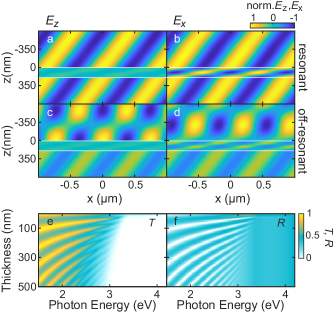
The electron’s incident angle was at first chosen to be normal to the silicon film and the incident angle of the light field was fixed at , unless otherwise stated. Considering a thin film thickness of nm, two exemplary distributions for the and -component of the electric field are plotted in Fig. 2(a,b) for a case in which Fabry-Perot modes are resonantly excited (illumination wavelength nm) and in Fig. 2(c,d) for an off-resonant case ( nm) respectively. The Fabry-Perot resonances are governed by the relation , where is the angle of the light inside the material relative to the surface normal and is an integer number.
In the resonant case, the transmission is large and the electric field in front of the thin film (region (1)) is dominated by the incident wave which interferes with a much weaker reflected field. Behind the thin film (region (3)) the field is described by a single monochromatic propagating wave phase-shifted with respect to the incident optical field. In the non-resonant case the reflected field in region (1) is much stronger leading to a pronounced checker-board field distribution due to interference with the incident field. Below the film (region (3)) the transmitted field is a single propagating plane wave again. Inside the material, off-resonant excitation leads only to weak fields, so that electron-light scattering is mostly determined by the fields outside of the material (region 1 and 3). However, at Fabry-Perot-Resonances enhances field amplitudes can occur inside the material affecting the overall electron-light coupling strength.
The transmittivity and reflectivity,
calculated for a broad spectrum of photon energies and different material thicknesses are plotted in Figure 2(e,f). Both quantities show a strong dependence on the material thickness as well as the photon energy. For energies larger than the direct band gap of silicon (about 3 eV), the transmission drops significantly due to the onset of lights absorption, whereas for energies smaller than the band gab transmittivity and reflectivity are heavily dominated by the influence of Fabry-Perot resonance modes in the thin film. Specifically, for thickness and wavelength combinations fulfilling the resonance condition, a pronounced decrease in the reflection and an increase in the transmission are observed.
3 Scattering of electrons at modulated -fields
The linear interaction between a moving electron and an optical near-field can be described semi-classically using the following interaction Hamiltonian in the Coulomb gauge:
| (1) |
where is the electron charge, the electron mass, is the vector potential of the optical field and the electron momentum operator.
Excerpt of general formalism
As previously discussed 16, 14, 19, the quantum mechanical state of the electron after leaving the light field can be described by an infinite number of energy ladder states equally spaced by the photon energy, with the occupation probabilities given by:
| (2) |
where is the index of the ladder state and corresponds to the number of net absorbed or emitted photons after the interaction. is the -th order Bessel function of the first kind. The dimensionless coupling constant is given by
| (3) |
where is the (real-space) Fourier transform of the electric field along the electron trajectory, here taken along the -direction. In Eq. 3 we have , which equals the momentum transfer experienced by an electron with velocity when it absorbs or emits a photon with frequency from the optical near-field.
Application: Scattering off Fabry-Perot pattern
In the following, we apply this general formalism to our case. Specifically, the Fourier transform of the optical field at a thin film can be decomposed into additive complex-valued contributions from truncated plane waves in each of the three regions (1) to (3), propagating in the forward () or backward () direction (see Supplemental Information 1). Since for electrons in vacuum , we are always in non-phase-matched conditions and the analytical solutions for the Fourier transforms are obtained as:
| (4a) | |||
| (4b) | |||
| (4c) | |||
in which are the z-components in the electron reference frame of the individual field components shown in Fig. 1(b). For the silicon thin film model described above, the individual contributions from each truncated plane wave is shown in Figure 3(a-j) for a film thickness of nm and photon energies in the visible spectral range and an incident field strength of V/m.
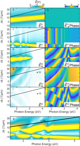
The incident field Fourier transform (Fig. 3a) is peaked along the light line . For the incident light truncated at the interface, the light line is broadened, leading to non-zero components at the position of the electron momentum change condition (black line). The amplitude of the incident component is independent of the refractive index of the sample and scales with (Eq. 4a) with no phase variation (Fig. 3b). Equivalently, for the reflected field component , maximum Fourier amplitudes are found at the light line of the reflected wave but now exhibiting pronounced variations due to changes in the reflectivity (Fig. 3c) associated with Fabry-Perot resonances. Overall, the coupling of the reflected wave is generally weaker in our geometry since in the denominator becomes large compared to in the denominator of the incident fields contribution (Eq. 4a). Qualitatively this can be understood because the reflected field is counter-propagating with respect to the electron which suppresses an effective coupling. The phase of the reflected fields contribution (Fig. 3d) is also dominated by the influence of the Fabry-Perot modes with phase jumps of at the resonance positions.
Also the transmitted field contribution (Fig. 3e) is dependent on the photon energy with the same resonance features as in the reflected field but with a sharp cutoff at the position of the band gap. Furthermore, an additional phase factor (Eq. 4c) is introduced due to the phase shift of the transmitted electrical field compared to the incident field. Hence the phase (Fig. 3f) has not only a photon energy dependence due to the Fabry-Perot modes but also a pronounced dependence.
The contributions from the electric fields inside the thin film (Fig. 3(g,i)) are smaller by one order of magnitude as compared to the influence of the fields outside the material due to dielectric screening and the normal electron incident () considered here. Both Fourier transforms, , are dominated by sinc-like fringes stemming from the rectangular profile of the real space electric fields with corresponding phase jumps (Fig. 3(h,j)). The combination of all contributions, as depicted in Fig. 3k, is mainly dominated by the contributions from , and .
4 Electron-light coupling strength
Neglecting the field within the film and expressing the field amplitudes via their analogues in the thin films rotated frame (see Supplemental Information 1) and then replacing them by the reflection and transmission coefficients and , the overall coupling strength according to Eq. 3 can be written as:
| (5) | ||||
Eq. 5 with , retrieves the expression for the special case of electron-light coupling at a perfect conductor interface derived in Ref.20.
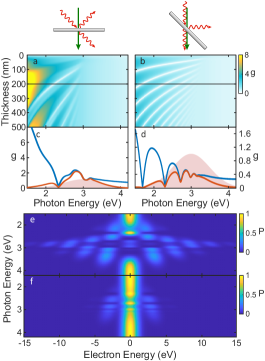
We calculated the coupling strength for a variety of thin film thicknesses depicted in Figure 4a. In comparison to the reflectivity and transmittivity in Figure 2 the overall coupling strength does not directly resemble the optical features of the thin film. The Fabry-Perot resonances become partially masked by the influence of the interference term in equation 5 as a result of the phase shift between the fields in front and behind the thin film.
To increase the visibility of the Fabry-Perot modes the coupling to the reflected field would need to be increased while at the same time the coupling to the incident and transmitted field should be suppressed. This can be achieved by changing the lights incident angle and the thin films tilt angle . Adjusting the angles and , the first term in equation 5 vanishes and the resulting coupling strength, plotted in Figure 4b, is now solely dependent on the reflectivity (In fact also the contribution from the field inside the material becomes larger but the overall characteristics are dominated by the reflected field outside the material (see Supplemental Information 2)). This emphasizes the possibility of the PINEM technique to map optical properties directly onto the electron photon coupling.
Further discussion
To further elucidate this and to give and example for a possible experimental realization we extract the electron-light coupling strength for a thin film thickness of nm (Fig. 4c). The coupling between electrons and photons decreases in general with increasing photon energy and has some specific minima and maxima. In an experimental frame a strongly chirped laser pulse could be used together with an ultrashort electron probe pulse to monitor the coupling strength at a specific instantaneous photon frequency by adjusting the relative arrival time of both pulses. Therefore we multiplied the coupling strength with a Gaussian to emulate the temporal pulse form (Fig. 4d) and calculated the electron energy sideband occupation probability (electron energy distribution after interaction) for every photon energy resulting in a PINEM spectrogram (Fig. 4e). The photon energy dependent modulation of the coupling strength leads to a decrease and increase of the sideband population if a material resonance is present.
5 Conclusion
We derived an analytical expression for the strength of electron-photon scattering at a thin film illuminated by an incident optical field, by using a matching matrix approaches. We calculated the transversal electric field components of the incident and reflected field amplitudes in front, inside and behind the thin film and performing an analytical Fourier transform. The results give insight on how the overall electron-light coupling results from the coupling to the electric fields in the different regions. By altering the incident angles of the electrons and the light field the influence of certain components can be reduced or enhanced. This is useful since certain components carry information about the optical response of the thin film. By choosing optimized angles and applying strongly chirped optical fields, it should be possible to map material depended resonances directly onto the electron sideband population in a PINEM experiment.
6 Acknowledgment
We acknowledge financial support by the DFG within the priority program 1840 ”Quantum Dynamics in Tailored Intense Fields”, funding by the Volkswagen Foundation as part of the Lichtenberg Professorship ”Ultrafast nanoscale dynamics probed by time-resolved electron imaging” and funding by the Free State of Bavaria through the Lighthouse project ”Free-electron states as ultrafast probes for qubit dynamics in solid-state platforms” within the Munich Quantum Valley initiative.
7 Author Contributions
N.M. and S.S. jointly developed the theoretical model. N.M. and S.S. conducted the numerical simulations with the help of G.V.. N.M. and S.S. wrote the manuscript with the help of F.E..
7.1 Supporting information
Supporting information: Optical field distribution at a thin film, Choosing the angles and (PDF)
References
- Hawkes and Spence 2019 Hawkes, P. W.; Spence, J. C. Springer handbook of microscopy; Springer Nature, 2019
- Dömer and Bostanjoglo 2003 Dömer, H.; Bostanjoglo, O. High-speed transmission electron microscope. Rev. Sci. Instrum. 2003, 74, 4369–4372
- Zewail 2010 Zewail, A. H. Four-dimensional electron microscopy. Science 2010, 328, 187–193
- Piazza et al. 2013 Piazza, L.; Masiel, D.; LaGrange, T.; Reed, B.; Barwick, B.; Carbone, F. Design and implementation of a fs-resolved transmission electron microscope based on thermionic gun technology. Chem. Phys. 2013, 423, 79–84
- Feist et al. 2017 Feist, A.; Bach, N.; da Silva, N. R.; Danz, T.; Möller, M.; Priebe, K. E.; Domröse, T.; Gatzmann, J. G.; Rost, S.; Schauss, J. Ultrafast transmission electron microscopy using a laser-driven field emitter: Femtosecond resolution with a high coherence electron beam. Ultramicroscopy 2017, 176, 63–73
- Baum et al. 2007 Baum, P.; Yang, D.-S.; Zewail, A. H. 4D visualization of transitional structures in phase transformations by electron diffraction. Science 2007, 318, 788–792
- Barwick et al. 2008 Barwick, B.; Park, H. S.; Kwon, O.-H.; Baskin, J. S.; Zewail, A. H. 4D imaging of transient structures and morphologies in ultrafast electron microscopy. Science 2008, 322, 1227–1231
- Cremons et al. 2016 Cremons, D. R.; Plemmons, D. A.; Flannigan, D. J. Femtosecond electron imaging of defect-modulated phonon dynamics. Nat. Commun. 2016, 7, 11230
- Feist et al. 2018 Feist, A.; Rubiano da Silva, N.; Liang, W.; Ropers, C.; Schäfer, S. Nanoscale diffractive probing of strain dynamics in ultrafast transmission electron microscopy. Struct. Dyn. 2018, 5, 014302
- Danz et al. 2021 Danz, T.; Domröse, T.; Ropers, C. Ultrafast nanoimaging of the order parameter in a structural phase transition. Science 2021, 371, 371–374
- Rubiano da Silva et al. 2018 Rubiano da Silva, N.; Möller, M.; Feist, A.; Ulrichs, H.; Ropers, C.; Schäfer, S. Nanoscale Mapping of Ultrafast Magnetization Dynamics with Femtosecond Lorentz Microscopy. Phys. Rev. X 2018, 8, 031052
- Berruto et al. 2018 Berruto, G.; Madan, I.; Murooka, Y.; Vanacore, G.; Pomarico, E.; Rajeswari, J.; Lamb, R.; Huang, P.; Kruchkov, A.; Togawa, Y.; others Laser-induced skyrmion writing and erasing in an ultrafast cryo-Lorentz transmission electron microscope. Phys. Rev. Lett. 2018, 120, 117201
- Barwick et al. 2009 Barwick, B.; Flannigan, D. J.; Zewail, A. H. Photon-induced near-field electron microscopy. Nature 2009, 462, 902–906
- Park et al. 2010 Park, S. T.; Lin, M.; Zewail, A. H. Photon-induced near-field electron microscopy (PINEM): theoretical and experimental. New J. Phys. 2010, 12, 123028
- García de Abajo 2010 García de Abajo, F. J. Optical excitations in electron microscopy. Ref. Mod. Phys. 2010, 82, 209–275
- García de Abajo et al. 2010 García de Abajo, F. J.; Asenjo-Garcia, A.; Kociak, M. Multiphoton absorption and emission by interaction of swift electrons with evanescent light fields. Nano Lett. 2010, 10, 1859–1863
- Piazza et al. 2015 Piazza, L.; Lummen, T.; Quinonez, E.; Murooka, Y.; Reed, B.; Barwick, B.; Carbone, F. Simultaneous observation of the quantization and the interference pattern of a plasmonic near-field. Nat. Commun. 2015, 6, 6407
- Kurman et al. 2021 Kurman, Y.; Dahan, R.; Sheinfux, H. H.; Wang, K.; Yannai, M.; Adiv, Y.; Reinhardt, O.; Tizei, L. H.; Woo, S. Y.; Li, J. Spatiotemporal imaging of 2D polariton wave packet dynamics using free electrons. Science 2021, 372, 1181–1186
- Feist et al. 2015 Feist, A.; Echternkamp, K. E.; Schauss, J.; Yalunin, S. V.; Schäfer, S.; Ropers, C. Quantum coherent optical phase modulation in an ultrafast transmission electron microscope. Nature 2015, 521, 200–203
- Vanacore et al. 2018 Vanacore, G. M.; Madan, I.; Berruto, G.; Wang, K.; Pomarico, E.; Lamb, R. J.; McGrouther, D.; Kaminer, I.; Barwick, B.; García de Abajo, F. J.; Carbone, F. Attosecond coherent control of free-electron wave functions using semi-infinite light fields. Nat. Commun. 2018, 9, 2694
- Dahan et al. 2020 Dahan, R.; Nehemia, S.; Shentcis, M.; Reinhardt, O.; Adiv, Y.; Shi, X.; Be’er, O.; Lynch, M. H.; Kurman, Y.; Wang, K.; Kaminer, I. Resonant phase-matching between a light wave and a free-electron wavefunction. Nat. Phys. 2020, 16, 1123–1131
- Reinhardt and Kaminer 2020 Reinhardt, O.; Kaminer, I. Theory of Shaping Electron Wavepackets with Light. ACS Photonics 2020, 7, 2859–2870
- Feist et al. 2020 Feist, A.; Yalunin, S. V.; Schäfer, S.; Ropers, C. High-purity free-electron momentum states prepared by three-dimensional optical phase modulation. Phys. Rev. Res. 2020, 2, 043227
- Kfir et al. 2020 Kfir, O.; Lourenço-Martins, H.; Storeck, G.; Sivis, M.; Harvey, T. R.; Kippenberg, T. J.; Feist, A.; Ropers, C. Controlling free electrons with optical whispering-gallery modes. Nature 2020, 582, 46–49
- Henke et al. 2021 Henke, J.-W.; Raja, A. S.; Feist, A.; Huang, G.; Arend, G.; Yang, Y.; Kappert, F. J.; Wang, R. N.; Möller, M.; Pan, J.; Liu, J.; Kfir, O.; Ropers, C.; Kippenberg, T. J. Integrated photonics enables continuous-beam electron phase modulation. Nature 2021, 600, 653–658
- Kfir 2019 Kfir, O. Entanglements of electrons and cavity photons in the strong-coupling regime. Phys. Rev. Lett. 2019, 123, 103602
- Ben Hayun et al. 2021 Ben Hayun, A.; Reinhardt, O.; Nemirovsky, J.; Karnieli, A.; Rivera, N.; Kaminer, I. Shaping quantum photonic states using free electrons. Sci, Adv. 2021, 7, eabe4270
- Dahan et al. 2021 Dahan, R.; Gorlach, A.; Haeusler, U.; Karnieli, A.; Eyal, O.; Yousefi, P.; Segev, M.; Arie, A.; Eisenstein, G.; Hommelhoff, P.; Kaminer, I. Imprinting the quantum statistics of photons on free electrons. Science 2021, 373, eabj7128
- Feist et al. 2022 Feist, A.; Huang, G.; Arend, G.; Yang, Y.; Henke, J.-W.; Raja, A. S.; Kappert, F. J.; Wang, R. N.; Lourenço-Martins, H.; Qiu, Z.; Liu, J.; Kfir, O.; Kippenberg, T. J.; Ropers, C. Cavity-mediated electron-photon pairs. Science 2022, 377, 777–780
- Schinke et al. 2015 Schinke, C.; Christian Peest, P.; Schmidt, J.; Brendel, R.; Bothe, K.; Vogt, M. R.; Kröger, I.; Winter, S.; Schirmacher, A.; Lim, S. Uncertainty analysis for the coefficient of band-to-band absorption of crystalline silicon. Aip Adv. 2015, 5
- Vogt 2016 Vogt, M. R. Development of physical models for the simulation of optical properties of solar cell modules. Ph.D. thesis, Leibnitz Universität Hannover, 2016
- Orfanidis 2002 Orfanidis, S. J. Electromagnetic waves and antennas; 2002