Kramers nodal line in the charge density wave state of YTe3 and the influence of twin domains
Abstract
Recent studies have focused on the relationship between charge density wave (CDW) collective electronic ground states and nontrivial topological states. Using angle-resolved photoemission and density functional theory, we establish that YTe3 is a CDW-induced Kramers nodal line (KNL) metal, a newly proposed topological state of matter. YTe3 is a non-magnetic quasi-2D chalcogenide with a CDW wave vector () of 0.2907c∗. Scanning tunneling microscopy and low energy electron diffraction revealed two orthogonal CDW domains, each with a unidirectional CDW and similar . The effective band structure (EBS) computations, using DFT-calculated folded bands, show excellent agreement with ARPES because a realistic x-ray crystal structure and twin domains are considered in the calculations. The Fermi surface and ARPES intensity plots show weak shadow bands displaced by from the main bands. These are linked to CDW modulation, as the EBS calculation confirms. Bilayer split main and shadow bands suggest the existence of crossings, according to theory and experiment. DFT bands, including spin-orbit coupling, indicate a nodal line along the line from multiple band crossings perpendicular to the KNL. Additionally, doubly degenerate bands are only found along the KNL at all energies, with some bands dispersing through the Fermi level.
I Introduction
Understanding of the coupling between collective electronic ground states such as charge density wave (CDW) or superconductivity and non-trivial topology has become an exciting research frontier in the field of condensed matter physics [1, 2, 3, 4, 5, 6, 7, 8, 9, 10, 5]. The intricate interplay of CDW and the non-trivial band topology often gives rise to various exotic topological phases such as an axion insulator state [3], Kramers nodal line (KNL) metal [1], quantum spin-Hall insulator [4], fractional Chern insulator states [8], eightfold fermionic quasiparticle [9] and manipulation of topologically protected states [10, 5], to mention a few.
CDW is typically observed in layered materials exhibiting quasi-one dimensional (quasi-1D) or quasi-two dimensional (quasi-2D) structures. Due to the associated modification in lattice symmetry, CDW can drive topological phase transitions [1, 7, 10, 3]. For instance, we have recently demonstrated that CDW induced inversion symmetry breaking gives rise to a KNL [11] in the non-magnetic layered rare-earth tritelluride, LaTe3 [1]. KNLs are new type of two-fold degenerate nodal lines that always connect two time reversal invariant momenta (TRIM) of the Brillouin zone (BZ) and are robust under spin-orbit coupling (SOC) [11]. Xie et al. have proposed that all non-centrosymmetric achiral crystal symmetries with sizable SOC, when coupled with time reversal (TR) symmetry, should host this KNL state [11]. Besides our recent work on LaTe3 [1], experimental evidence of KNL is limited to ruthenium silicides [12] and SmAlSi [13].
Yttrium tritelluride (YTe3) is another member of the RTe3 series (R= rare earth) that is non-magnetic and exhibits an incommensurate CDW state at ambient temperature [14, 15, 16, 17]. As in other RTe3 compounds, it has a structure consisting of R-Te1 corrugated blocks sandwiched between the Te2-Te3 bilayers along the long axis () [Fig. 1(a)]. The Te bilayers in YTe3 host the CDW [14, 15]. The CDW transition temperature (TCDW) of 334 K has been determined from resistivity measurements [18]. The magnetization measurements conducted on YTe3 indicate that the diamagnetic susceptibility remains unchanged up to the room temperature [14]. The non-magnetic nature of YTe3 indicates the existence of TR symmetry. YTe3 exhibits an orthorhombic structure in the non-CDW state above TCDW, characterized by the space group [14]. However, in contrast to the other members of RTe3 series (R: La-Tm), whose detailed x-ray crystallography study in the CDW state is reported in literature [17], the structure of YTe3 has not been studied. An angle-resolved photoemission spectroscopy (ARPES) investigation on YTe3 [15] reported a -dependent (in-plane) variation of the CDW gap, where the gap decreases as increases. Their study suggests a smaller CDW gap and consequently a smaller gapped region in the Fermi surface (FS) in YTe3 compared to LaTe3. An interesting characteristic of YTe3 is that it exhibits superconductivity with a transition temperature of ∼3 K with 8% Pd intercalation, which in turn, inhibits the CDW state [19].
The existence of the CDW and resemblance of the physical properties with LaTe3 motivated us to perform a comprehensive study of YTe3. At the first step, the structure of YTe3 in the CDW phase was solved by x-ray crystallography. Two mutually orthogonal incommensurate CDW domains with similar CDW wave vector () values observed in scanning tunneling microscopy (STM) and low energy electron diffraction (LEED) significantly modifies the ARPES intensity plots and the Fermi surface. Effective band structure (EBS) calculations based on density functional theory (DFT) considering the twin domains and using a realistic structure of the CDW state determined by x-ray crystallography provide excellent agreement with ARPES, which shows faint bilayer split shadow bands that show potential crossing with the main bands. DFT calculations show formation of KNL along the line characterized by doubly degenerate bands along the KNL and crossings perpendicular to it.
II Methods
II.1 Experimental:
Single crystals of YTe3 with residual resistivity ratio [RRR, (300 K)/(2 K)] of 32 were grown using the tellurium flux method [20]. High-purity Y and Te were mixed in a molar ratio of 1:39. This mixture was sealed under high vacuum in a crucible and heated at 900∘C for 10 h, and subsequently cooled slowly to 600∘C in 4 days. Excess Te was separated using a high-temperature centrifuge, resulting in gold-colored, plate-like YTe3 crystals.
Single-crystal x-ray diffraction data for YTe3 were collected at 100 K with the use of graphite-monochromatized MoK radiation (= 0.71073 Å) STOE IPDS diffractometer. The collection of intensity data as well as cell refinement and data reduction were carried out with the use of the program X-Area. An analytical absorption correction was performed (X-Shape within X-Area) and the modulated structure was refined with JANA2006 [21]. Atomic coordinates of the atoms in the subcell and initial values of their modulation functions were determined by the charge-flipping method [22, 23]. The distortion (positional or displacement parameter) of a given atomic parameter in the subcell was expressed by a periodic modulation function () in a form of a Fourier expansion = sin+cos, where is the sinusoidal coefficient of the given Fourier term, the cosine coefficient, the number of modulation waves used for the refinement and the lattice translation. = , where are integer numbers for the linear combination of the incommensurate modulation vectors . Satellite reflections of one order were observed and used for the refinement. Consequently, one modulation wave for positional and thermal parameters was used for all atoms. Only the symmetry allowed Fourier terms were refined.
The ARPES measurements were conducted at the SGM3 beamline at the ASTRID2 synchrotron facility [24]. FS data at the SGM3 beamline were collected with an energy resolution of 15-20 meV at photon energies (h) of 24 and 28 eV, with an angular resolution of 0.2∘ (0.008 Å-1). These measurements were performed at various temperatures ranging from 45-340 K, and photon energy-dependent studies were conducted using different photon energies in the range of 16 eV to 30 eV. A linearly polarized photon beam in the horizontal plane was incident at an angle of 50∘ with respect to the surface normal, which was oriented along the analyzer axis. The analyzer slit was vertically oriented, resulting in a vertical detection plane, the experimental geometry is similar to what has been used in Ref. 1. The STM measurements were conducted under a base pressure of 210-11 mbar employing a variable-temperature STM from Omicron Nanotechnology GmbH in the constant current mode. Mechanincally grinded Pt-Ir tips from Unisoku were used and cleaned in-situ using voltage pulse method. LEED was performed using a four grid rear view optics from OCI Vacuum Microengineering. A third order 2D polynomial background function (with 10 coefficients) [25] was subtracted from the LEED image to extract the weak CDW related satellite spots. All the measurements were carried out on freshly peeled surfaces under a chamber base pressure of 210-10 mbar.
II.2 Density functional theory:
DFT calculations have been performed using the Vienna Ab-initio Simulation Package (VASP) [26, 27] within the framework of the projector augmented wave method (PAW) [26, 27] to obtain the electronic structure of YTe3. The exchange-correlation functional is treated under the generalized gradient approximation [28]. The energy cut-off is set to 500 eV for the expansion of the plane waves. The convergence criterion for energy in the self-consistent-field cycle and total force tolerance on each atom are taken to be 10-6 eV and 0.02 eV/Å, respectively. The SOC is employed by a second-variation method as implemented in the VASP code [27]. The calculations have been performed for a seven-fold approximate structure with C2cm space group (SG #40) derived from the experimental atomic positions from the cif file using the PSEUDO program [29]. This program displaces the atoms to arrive at the commensurate seven-fold structure with non-centrosymmetric space group (SG #40). This is discussed further in section III.1.
EBS has been computed using Pyprocar code and experimental energy and momentum broadening were convoluted with the unfolded spectral function for comparison with ARPES [1, 30]. All the DFT bands (and consequently the EBS) are rigidly shifted to larger binding energy () by 0.1 eV with respect to the for comparison with the ARPES data. VESTA software has been used for crystal structure visualization [31].
III Results and Discussion
III.1 Crystal structure of YTe3 in the CDW state
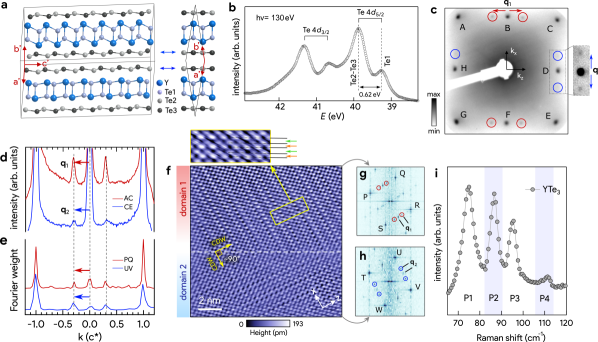
X-ray crystallography data show that YTe3 has an orthorhombic structure. The lattice constants and other crystal data are presented in Table S1 of the Supplementary Material (SM) [32]. We find that YTe3 hosts a unidirectional incommensurate CDW with the = 0.2907c∗ and the superspace group is determined to be (00), similar to the other members of the RTe3 series [17]. is the basic space group of the (00) superspace group and represents the component of .
An incommensurate structure is generally approximated as a commensurate structure with a large unit cell such that its is close to the incommensurate value. However, the latter becomes an accurate representation of the incommensurate structure if it is based on the atom positions determined by x-ray crystallography and the value is within the experimental accuracy [33, 34]. By utilizing the continued fraction method [35] to find a rational fraction that could represent , we arrive at a fiftyfive-fold structure (1155 supercell) with C2cm space group with = 16/55c∗ = 0.2909c∗ that matches the experimental value of 0.2907(4)c∗ within its accuracy. It has 440 atoms in the unit cell with positions almost coinciding with those given by x-ray crystallography. A comparison of the Te2 and Te3 atom positions (green dots) with the experimental positions (open circles) show no perceptible deviation [Fig. S1(a) of SM [32]]. This is also supported by a small average displacement (= 0.001 Å) of the atoms in the unit cell from the experimentally determined positions, as obtained from the PSEUDO program [29].
However, because of the large size of the fiftyfive-fold unit cell, DFT calculations turned out to be highly resource intensive. So, a smaller seven-fold unit cell with 56 atoms is derived, importantly with all symmetries of the fiftyfive-fold structure preserved i.e., with the same space group [Fig. 1(a)]. The corresponding value is 2/7 (= 0.2857), which is an 1.8% deviation from the experimental value, with the Te atoms (orange dots) showing small deviations from the experimental positions (open circles) [Fig. S1(b) of SM [32]]. Figure 1(a) shows that YTe3 is made up of two main structural units: the Te2-Te3 bilayer that hosts the CDW and the Y-Te1 corrugated slab. The Te bilayer, highlighted by blue double-sided arrows, is weakly coupled by van der Waals interaction.
Te 4 core-level photoemission spectrum of YTe3 in Fig. 1(b) comprises of 4 and 4 peaks separated by the spin-orbit splitting of ∼1.5 eV. Note that each of these peaks exhibit two components that are separated by ∼0.6 eV. These components are the signature of different valency of Te in the Y-Te1 slab and the Te2-Te3 layer due to transfer of electronic charge from the former to the latter. A nearly similar splitting was observed in LaTe3 4 [1] and 3 [36] spectra. This was attributed to the difference in valencies of Te1 compared to Te2 (and Te3), as supported by the DFT calculations.
III.2 Twin domains on the YTe3 surface
In Fig. 1(c), the LEED pattern of the YTe3 surface in the CDW state at room temperature (the CDW transition temperature being 334 K [18]) displays sharp main spots labeled as A-H. The satellite spots related to the CDW modulation along the direction are highlighted by red circles. Interesting to note are the relatively weaker satellite spots in the direction (blue circles). These are unambiguously visible after performing a background subtraction, as shown in the inset on the right side. The CDW modulation vectors along and along have been determined from the LEED intensity profiles by measuring the distance between the satellite and the main peaks. In Fig. 1(d), the intensity line profiles measured along AC and CE demonstrate that both and have similar value of (0.30.01), which is in agreement with that determined by x-ray crystallography. Note that for RTe3 with R= Tb-Tm, coexisting bidirectional CDW has been observed [37, 16, 38], and the magnitudes of in the two mutually perpendicular directions are different (e.g., (2/7)c∗ and (1/3)a∗ for ErTe3 [15, 39]). On the other hand, the values for the two twin domains are similar here for YTe3.
These twin domains are directly observed in the STM topography image with atomic resolution, where the domain boundary is indicated by a dashed white line [Fig. 1(f)]. Satellite spots related to the CDW are also visible in the Fourier transforms (FT) of each domain along and for domain 1 (top) and domain 2 (bottom), respectively [Figs. 1(g,h)]. In Fig. 1(e), the q values for the two domains from the line profiles measured along PQ [Fig. 1(g)] and UV [Fig. 1(h)] are = (0.29 0.03)c* and = (0.3 0.05)c*, which are equal within the error bar and are in excellent agreement with the values obtained from LEED. It was also noted from STM topographies performed at different sample locations that domain 1 is more prevalent compared to domain 2, a finding corroborated by the lower intensity of the LEED spots corresponding to domain 2 [Figs. 1(c)].
In Fig. 1(f), atomic resolution enables direct observation of the CDW in the top Te layer. A zoomed region in the yellow rectangle shows that the average positions of the neighboring Te chains, depicted by the black dashed lines, are not equidistant (orange and green arrows), signifying the breaking of mirror symmetry and, consequently, the inversion symmetry as well. The non-centrosymmetry is also demonstrated by the Raman spectrum in Fig. 1(i) through occurrence of P2 and P4 peaks of symmetry mode, which is an irreducible representation of achiral C2v point group. These modes were also observed in LaTe3 [1, 40]. The mirror symmetry however remains intact in the non-CDW state that has a centrosymmetric space group [14, 18].
III.3 Shadow branches in the twin domain modified Fermi surface
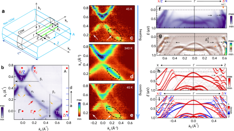
The Fermi surface in the CDW state of YTe3 measured by ARPES comprises two diamond-shaped sheets centered around and two smaller oval pockets – and – located near the and points, respectively; these high symmetry points are indicated by red color [Fig. 2(b)]. The high symmetry points are also shown in the Brillouin zone (BZ) (black lines) in Fig. 2(a), it is inscribed within the non-CDW BZ (cyan). A signature of a gapped region in the FS around the direction was observed previously for other RTe3 compounds [15, 1]. Curiously, such a gapped region seems to be absent in Fig. 2(b). The FS rather seems to nearly resemble that calculated for the non-CDW state of RTe3 [1, 15], except for an important difference: occurrence of a narrow gapped region, highlighted by the red arrow at (, ) = (0.2, 0.2) Å-1 that splits the inner diamond-shaped sheet (). We henceforth refer to the upper (lower) part as (), as shown in Fig. 2(b). resembles rotated by 90∘. A similar replica of the (upper part of the outer sheet) branch is named as (lower part). that is observed around Z in the lower right corner, is also a replica of the pocket around X (upper left corner).
The appearance of these replicas in the FS rotated by 90∘ can be explained by the presence of the twin domains (1 and 2) since the ARPES signal with a photon beam spot size of (200100) m2 probes both the domains simultaneously. The intensity of the FS branches related to domain 2 is less e.g., compare the intensities of the sheet and the sheet. This indicates that the contribution of domain 1 is greater than that of domain 2, which is consistent with the LEED and STM results discussed in the previous section. The high symmetry points of domain 1 (related to ) and domain 2 (related to ) are shown by red and blue colors, respectively in Fig. 2(b).
To examine whether the narrow gapped region (red arrow) mentioned above might be a signature of the CDW gap, we have measured the FS in both CDW and the non-CDW states. Interestingly, in contrast to the FS in the CDW state at 45 K [Fig. 2(c)], as the temperature is raised above [Fig. 2(d)], the sheet is no longer gapped at 340 K (black dashed oval), indicating CDW melting. Subsequently, as the temperature is lowered back to 45 K, the gap becomes visible again [white arrows in Fig. 2(e)]. Thus temperature dependent FS measurement establishes that the narrow gapped region in the sheet corresponds with the CDW gap in YTe3. Additionally, from a comparison of the ARPES bands and the calculated EBS considering both domains, we show how the combined effect of CDW gap and twin domains gives rise to the narrow gapped region in the FS in Discussion A of the SM [32].
Thus, unlike the case of RTe3 single crystals (as in Ref. 1), the FS of our YTe3 crystals is significantly modified by the presence of twin domains. In spite of this, shadow branches that are related to the CDW modulation are observed, as indicated by dark yellow arrows in Fig. 2(b). These are separated from the main branches by (black dashed arrows). The shadow branches are observed for both the domains; see for example, the vertical and horizontal black dashed arrows of length .
III.4 ARPES and effective band structure along XZ
The ARPES intensity plot of YTe3 along XZ high-symmetry direction in Fig. 2(f) shows that the bands towards the () direction of domain 1 overlap with those of the () direction of domain 2. Therefore, the intensity plot seems to be essentially identical in these two directions, with bands crossing the in both directions. Additionally, in both the directions, some bands are bent away from the [black arrows] due to the hybridization of the main band and shadow band, resulting in formation of the CDW gap. In Fig. 2(g), these hybridized bands with enhanced clarity are shown by the black and orange arrows around = 0.3 eV and 0.5 eV, respectively. The lower limit of the CDW gap defined from the to the band maximum [], is estimated to be 0.290.02 eV. This value is similar in both directions.
In Fig. 2(h), the DFT calculated bands of YTe3 along for the seven-fold structure show multiple folded bands along both and directions (gray dashed curves), which are difficult to compare with the ARPES intensity plots [Figs. 2(f,g)]. So, we have determined the EBS from the DFT bands by band unfolding, as shown by the red markers [1, 42, 43]. The EBS shows reasonable resemblance with ARPES: The CDW gap along is evident in the EBS, as marked by the black arrows in Fig. 2(h). Along , two parabolic bands (related to the pocket) centered around X cross the , along with two additional bands (related to the sheet) that approach the .
The agreement between theory [Fig. 2(i)] and experiment [Fig. 2(g)] is excellent when the influence of the twin domains is accounted for by superimposing the EBSs calculated along and , where the red and blue bands represent the domain 1 and 2 bands, respectively. For 0, the bands involved in the CDW gap formation are from domain 1, while the bands that cross are from domain 2. The roles are reversed for 0. Figure S2 of SM [32] shows the evolution of the CDW gap across the BZ; a good agreement of ARPES and EBS is also apparent here, see Discussion A of SM [32].
III.5 Main and Shadow bands towards near the BZ boundary
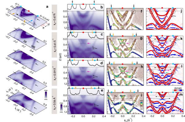
In this subsection, we investigate the interaction between the ARPES main bands that are present also in the non-CDW state and shadow bands that only appear in the CDW state. Fig. 3(a) shows a stack of - isosurface plots for different ranging from = 0 to 0.4 eV. The FS i.e., the top plot for = 0 as well as other isosurface plots at larger show the shadow branches corresponding to the main branch, as indicated by yellow arrows. The main and shadow branches appear to cross, and the crossing point shifts to lower as increases (shown by the black arrows). Notably, the crossing point does not shift in and occurs at = 0.209 Å-1, (blue dashed arrow). Additionally, the crossings between the main and shadow bands are also identified in the ARPES intensity plots, (), measured at = 0.67, 0.61, 0.59, and 0.56 Å-1, respectively [Figs. 3(b-e)]. The red horizontal lines on the right axis of the FS in Fig. 3(a) indicate these directions. In Fig. 3(b), we observe two main bands (inner and outer) of parabolic shape that are centered around the point (indicated by the red dot at the top horizontal axis). These bands intersect at 0.15 and 0.21 Å-1. The outer main band related to the main branch disperses down to an energy of 1.2 eV, while the inner main band related to the main branch has the minimum at 0.8 eV. With decreasing in Figs. 3(c-e), the outer main band spreads out in , while the inner bands shrink in and its bottom moves towards lower . Additionally, a flat band at = 0.3 eV [pink arrows in Figs. 3(c,d) and (g,h)] along with a M-shaped band centered around = 0 [green arrow in Fig. 3(h), dashed black curve is guide to the eye] partly overlap with the main bands.
From the EBS in Figs. 3(j-m) [calculated at same values as in Figs. 3(f-i), respectively], where bands of both the domains are overlaid, we find that these additional bands (blue color) are related to domain 2 [pink and green arrows in Fig. 3(l)]. Furthermore, EBS reveals a splitting in main band, as highlighted by double black arrows in Fig. 3(k). This splitting – referred to as “bilayer splitting”– occurs due to the interaction between the Te bilayers that host the CDW in YTe3 and has been observed in other RTe3 members [1, 15, 44, 45]. Additionally, the calculated band structure at = 0.59 Å-1(gray curves in Fig. S3 of SM [32]) illustrates that the bilayer splitting for the outer main band increases with energy. For example, at = 0 eV, the splitting () is 0.2 Å-1, while at = 0.4 eV, it is 0.3 Å-1. Note that bilayer splitting is not related to the CDW, as has been discussed in detail for LaTe3 [1]. For YTe3 also, a comparison of the CDW band structures with the non-CDW state (blue dashed) in Fig. S3 of SM [32] reveals that the bilayer splitting is comparable in both states.
The ARPES intensity plots are however complicated by the presence of twin domains, bands from domain 2 interfere with the bands from domain 1. For example, some of the blue bands from domain 2 can be seen in between the bilayer split main bands and overlapping with the crossing region within the black dashed circles in Figs. 3(k-m). Nevertheless, bilayer splitting is observed at higher , where it is pronounced [two black arrows in Figs. 3(c-e) and (g-i)].
The evidence of shadow bands is obtained in the 2D curvature plots e.g., in Figs. 3(g-i). The shadow bands on both sides of the X point are separated by from the corresponding main bands, as shown by the black dashed horizontal arrows. In the raw APRES intensity plots in Figs. 3(b-e), the momentum distribution curves (MDC) at the (gray filled circles) depicts the where the shadow bands cross (yellow vertical arrows). The larger intensity peaks in the MDC are related to the main bands (black vertical arrows). As decreases, the separation between the main and the shadow band increases, and their crossing – indicated by the black dashed circles – shifts to higher values. However, independent of , the crossings occur at same at the line [cyan dot at the top of Figs. 3(f-i)].
It may be noted that, in good agreement with ARPES, the calculated EBSs in Figs. 3(j-m) show that the shadow bands are separated by from the main bands, as indicated by the horizontal black dashed arrows. EBS clearly shows that the shadow bands in YTe3 are weaker than in LaTe3 [1], which is consistent with an observation from ARPES. So, this is not related to extraneous factors, but is related to the difference in the crystal structure of these two compounds. The most notable difference – although their are close – is in the amplitude () of the CDW modulation that is a factor of two smaller in YTe3 (= 0.07 Å from Fig. S1 of SM [32]) compared to LaTe3 (= 0.14 Å from the supplementary Fig. 2 of Ref. 1). Additionally, our EBS calculation for LaTe3 showed that if decreases to about one-fifth of the experimental value, the shadow bands are almost completely absent [1]. Thus, it is reasonable to conclude that the weakness of the shadow bands in YTe3 is related to the smaller amplitude of the CDW. In spite of this, the crossings of the shadow bands with the main bands are observed [highlighted by the black dashed circles in Figs. 3(j-m)]. These show similar trend as ARPES, i.e., the crossings move towards larger with lower .
III.6 Evidence of Kramers nodal line in YTe3
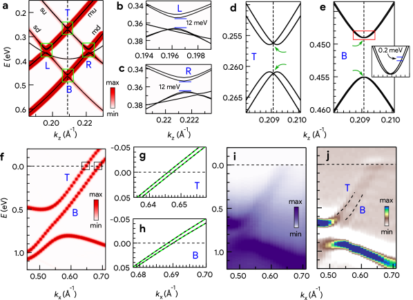
Figure 4(a) shows the EBS of the crossing region at = 0.59 Å-1 corresponding to the black dashed circle in Fig. 3(l). EBS shows four crossings (L, R, T and B) between the bilayer split main band (mu and md) and the shadow band (su and sd). Since the electronic structure of the structurally similar domains would be same, to avoid the interference from the bands of domain 2, we have shown the EBS for domain 1 only and the corresponding folded band structure (black curves) is overlaid on it. Note that the additional parabolic band due to band folding is not detected in the unfolded EBS because of its reduced spectral weight and is also not observed in ARPES [Figs. 3(d,h)]. Notably, although all the four crossings were observed from ARPES in LaTe3 [1], in case of YTe3 the weakness of shadow bands and interference of the twin domains make it difficult to identify them.
In Figs. 4(b,c), expanded regions near L and R crossings of YTe3 show that both are gapped by 12 meV. and also exhibit a mini gap (4-6 meV). To decipher the influence of SOC, we have calculated the folded band structure near the crossing region without SOC (Fig. S4 of SM [32]). Mini-gaps are observed at and without SOC, signifying the hybridization of bands involved in these crossings. In contrast, and exhibit gapless crossings without SOC. Thus nodal lines are formed at and that are gapped out with SOC. A similar behavior has been reported for LaTe3 [1]. When SOC is considered, each of the gapped branches of both and exhibit splitting that is expected in a noncentrosymmetric system such as YTe3. However, it is interesting to note that the bands cross at = 0.209 Å-1, as indicated by green arrows in Figs. 4(d,e). = 0.209 Å-1 is significant because it corresponds to the direction. The origin of the crossings is discussed later. The SOC splitting is more pronounced in case of bands at the crossing [2 meV, Fig. 4(d)] compared to the crossing [0.2 meV, inset of Fig. 4(e)].
In Fig. 4(f), the EBS along X2 direction shows the dispersion of T and B crossing related bands, i.e., these bands trace the crossings along the direction. However, due to the broadening used, we do not observe both the branches. Both the mini-gapped branches of T and B are however evident in the folded band structure shown zoomed in Figs. 4(g) and (h), respectively, where two doubly degenerate branches cross the . From the ARPES intensity plot and its 2D curvature plot in Figs. 4(i,j) towards the direction at = 0.209 Å-1, the T and B crossing related bands are experimentally observed. These cross at = 0.62 and 0.66 Å-1, respectively. It is worth mentioning that the EBS [Fig. 4(f)] exhibits excellent agreement with the ARPES bands in Figs. 4(i,j).
An analysis of the orbital texture of the EBS for = 0.59 Å-1 [Fig. 4(a)] in Figs. S5(a-c) of SM [32], shows that both the main and shadow bands are predominantly of Te – character near the crossing regions, while Te character becomes significant for E0.5 eV, indicating the 2D character of both the main and shadow bands. Further, the orbital textures of the EBS along [Fig. 4(f)] presented in Figs. S5(d-f) of SM [32] reveal that both T and B bands exhibit significant contributions from the in-plane Te orbitals ( and ), showcasing their 2D nature. However, above = 0.4 eV, there is some contribution in the T band.
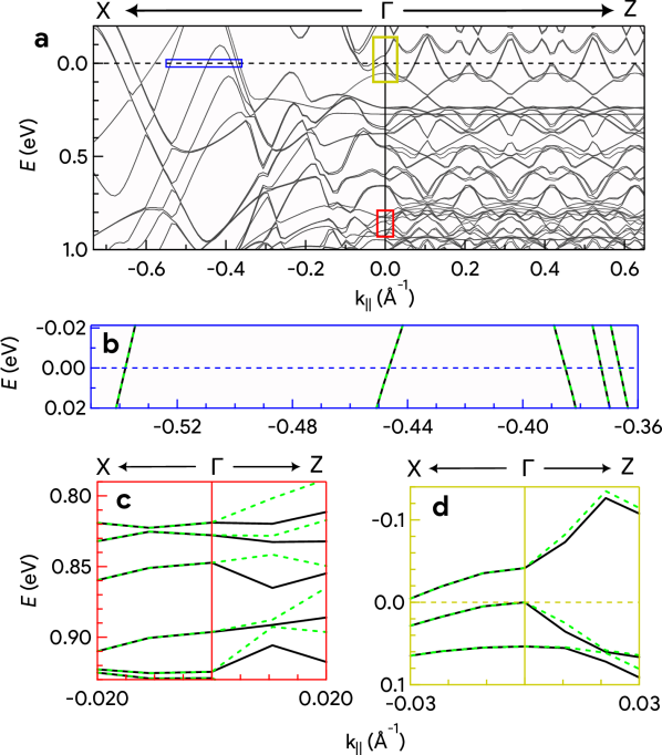
The double degeneracy of the bands discussed above is in fact true for all the DFT calculated bands along , as shown in Fig. 5. The zoomed blue rectangular region in Fig. 5(b) shows this for the different bands crossing the . The zoomed yellow and red rectangle regions in Figs. 5(c,d) show, in contrast, that the degeneracy is lifted by the SOC along other directions , along , whereas it remains in tact along both near and at larger , respectively. The seven-fold structure of YTe3 with C2cm space group and the little group that is isomorphic to point group, coupled with protection from time reversal symmetry, enforces the double degeneracy along , or the line [1]. This is the signature of the Kramers nodal line (KNL) [11] that always connects two TRIMs. In the present case, we find that both the upper and lower branches of and exhibit quadratic dispersion in the vicinity of the crossings [Figs. 4(d,e)]. This type of crossing with quadratic and cubic dispersion has been described as higher-order Dirac points (two fold degenerate) and the Berry phase around a KNL is quantized as m mod 2 [11]. The crossings of the CDW-induced shadow with the main bands are enforced by the KNL. The crossings of bands disperse and traverse the as increases [Figs. 4(f-j)] and multiple degenerate bands along the KNL cross [Figs. 5(a,b)] establishing that YTe3 is a KNL metal.
IV Conclusions
We present a comprehensive investigation of a non-magnetic chalcogenide material YTe3 in the CDW state combining results of the electronic band structure using ARPES, DFT performed with an experiment-based structure determined by x-ray crystallography and surface properties using STM and LEED. We find that the crystal structure of YTe3 is noncentrosymmetric with basic space group and of 0.2907c∗. A commensurate fiftyfive-fold structure is derived from the atomic positions determined by x-ray crystallography, which has a indistinguishable from the x-ray crystallography value within the experimental accuracy. However, since this unit cell is very large, the DFT calculations have been performed with a seven-fold structure, albeit with same symmetries.
Evidence of two mutually orthogonal CDW domains, each exhibiting an unidirectional and similar is obtained from both LEED and STM. The EBS, obtained by unfolding the DFT calculated bands, provides excellent agreement with ARPES when the contributions from both the twin domains are considered. The CDW gap is barely visible in the FS of YTe3 because of the twin domains. Nevertheless, the gap could be identified by comparing with the FS measured at high temperature in the non-CDW state. Thus, twin domains influence the band structure and the Fermi surface of YTe3.
CDW modulation related weak shadow bands near the BZ boundary, which are shifted from the main bands by , have been identified in ARPES intensity plots and are further corroborated by the EBS calculation. Additionally, possible existence of multiple crossings between the bilayer split main and shadow bands is portrayed both by experiment and theory. The bands calculated using DFT with SOC show a nodal line along resulting from the crossings between the bilayer split main and shadow bands perpendicular to the KNL. Doubly degenerate bands are found only along the KNL for all energy values, with certain bands crossing the . The KNL exists only in the CDW phase where shadow bands are present and the inversion symmetry is broken. The symmetries of the C2cm space group and the time reversal symmetry protect the KNL. Thus, our present work establishes that YTe3 is a KNL metal. The intricate interplay between CDW, non-trivial topology and twin domains in YTe3 unveils a rich landscape for further exploration and offers a pathway to deeper insights into exotic topological phases in condensed matter systems.
V Acknowledgments
S.S., P.S. and S.R.B. gratefully acknowledge the financial support from Department of Science and Technology, Government of India within the framework of the DST-Synchrotron-Neutron Project to perform experiments at ASTRID2 synchrotron facility. A part of this work was supported by VILLUM FONDEN via the Centre of Excellence for Dirac Materials (Grant No. 11744). H. S. Kunwar is thanked for help in the Raman measurement. The Computer division of Raja Ramanna Centre for Advanced Technology is thanked for installing the DFT codes and providing support throughout. At Argonne, this work was supported by the U.S. Department of Energy, Basic Energy Sciences, Office of Science, Materials Sciences and Engineering Division (synthesis, crystals growth, property characterization).
∗shuvamsarkarhere@gmail.com
†barmansr@gmail.com
References
- Sarkar et al. [2023] S. Sarkar, J. Bhattacharya, P. Sadhukhan, D. Curcio, R. Dutt, V. K. Singh, M. Bianchi, A. Pariari, S. Roy, P. Mandal, T. Das, P. Hofmann, A. Chakrabarti, and S. R. Barman, Charge density wave induced nodal lines in LaTe3, Nat. Commun. 14, 3628 (2023).
- Li et al. [2021] H. Li, T. T. Zhang, T. Yilmaz, Y. Y. Pai, C. E. Marvinney, A. Said, Q. W. Yin, C. S. Gong, Z. J. Tu, E. Vescovo, C. S. Nelson, R. G. Moore, S. Murakami, H. C. Lei, H. N. Lee, B. J. Lawrie, and H. Miao, Observation of unconventional charge density wave without acoustic phonon anomaly in kagome superconductors AV3Sb5 (, Cs), Phys. Rev. X 11, 031050 (2021).
- Shi et al. [2021] W. Shi, B. J. Wieder, H. L. Meyerheim, Y. Sun, Y. Zhang, Y. Li, L. Shen, Y. Qi, L. Yang, J. Jena, P. Werner, K. Koepernik, S. Parkin, Y. Chen, C. Felser, B. A. Bernevig, and Z. Wang, A charge-density-wave topological semimetal, Nat. Phys. 17, 381 (2021).
- Qian et al. [2014] X. Qian, J. Liu, L. Fu, and J. Li, Quantum spin hall effect in two-dimensional transition metal dichalcogenides, Science 346, 1344 (2014).
- Lei et al. [2021] S. Lei, S. M. L. Teicher, A. Topp, K. Cai, J. Lin, G. Cheng, T. H. Salters, F. Rodolakis, J. L. McChesney, S. Lapidus, N. Yao, M. Krivenkov, D. Marchenko, A. Varykhalov, C. R. Ast, R. Car, J. Cano, M. G. Vergniory, N. P. Ong, and L. M. Schoop, Band engineering of dirac semimetals using charge density waves, Adv. Mater. 33, 2101591 (2021).
- Yang and Kee [2010] B.-J. Yang and H.-Y. Kee, Searching for topological density-wave insulators in multiorbital square-lattice systems, Phys. Rev. B 82, 195126 (2010).
- Huang et al. [2021] S.-M. Huang, S.-Y. Xu, B. Singh, M.-C. Hsu, C.-H. Hsu, C. Su, A. Bansil, and H. Lin, Aspects of symmetry and topology in the charge density wave phase of 1t–TiSe2, New J. Phys. 23, 083037 (2021).
- Polshyn et al. [2021] H. Polshyn, Y. Zhang, M. A. Kumar, T. Soejima, P. Ledwith, K. Watanabe, T. Taniguchi, A. Vishwanath, M. P. Zaletel, and A. F. Young, Topological charge density waves at half-integer filling of a moiré superlattice, Nat. Phys. 18, 42 (2021).
- Zhang et al. [2020] X. Zhang, Q. Gu, H. Sun, T. Luo, Y. Liu, Y. Chen, Z. Shao, Z. Zhang, S. Li, Y. Sun, Y. Li, X. Li, S. Xue, J. Ge, Y. Xing, R. Comin, Z. Zhu, P. Gao, B. Yan, J. Feng, M. Pan, and J. Wang, Eightfold fermionic excitation in a charge density wave compound, Phys. Rev. B 102, 035125 (2020).
- Mitsuishi et al. [2020] N. Mitsuishi, Y. Sugita, M. S. Bahramy, M. Kamitani, T. Sonobe, M. Sakano, T. Shimojima, H. Takahashi, H. Sakai, K. Horiba, H. Kumigashira, K. Taguchi, K. Miyamoto, T. Okuda, S. Ishiwata, Y. Motome, and K. Ishizaka, Switching of band inversion and topological surface states by charge density wave, Nat. Commun. 11, 2466 (2020).
- Xie et al. [2021] Y.-M. Xie, X.-J. Gao, X. Y. Xu, C.-P. Zhang, J.-X. Hu, J. Z. Gao, and K. T. Law, Kramers nodal line metals, Nat. Commun. 12, 3064 (2021).
- Shang et al. [2022] T. Shang, J. Zhao, L.-H. Hu, J. Ma, D. J. Gawryluk, X. Zhu, H. Zhang, Z. Zhen, B. Yu, Y. Xu, Q. Zhan, E. Pomjakushina, M. Shi, and T. Shiroka, Unconventional superconductivity in topological Kramers nodal-line semimetals, Science Advances 8, eabq6589 (2022).
- Zhang et al. [2023] Y. Zhang, Y. Gao, X.-J. Gao, S. Lei, Z. Ni, J. S. Oh, J. Huang, Z. Yue, M. Zonno, S. Gorovikov, M. Hashimoto, D. Lu, J. D. Denlinger, R. J. Birgeneau, J. Kono, L. Wu, K. T. Law, E. Morosan, and M. Yi, Kramers nodal lines and weyl fermions in SmAlSi, Communications Physics 6, 10.1038/s42005-023-01257-2 (2023).
- Ru and Fisher [2006] N. Ru and I. R. Fisher, Thermodynamic and transport properties of , , and , Phys. Rev. B 73, 033101 (2006).
- Brouet et al. [2008] V. Brouet, W. L. Yang, X. J. Zhou, Z. Hussain, R. G. Moore, R. He, D. H. Lu, Z. X. Shen, J. Laverock, S. B. Dugdale, N. Ru, and I. R. Fisher, Angle-resolved photoemission study of the evolution of band structure and charge density wave properties in RTe3 (R=Y, La, Ce, Sm, Gd, Tb, and Dy), Phys. Rev. B 77, 235104 (2008).
- Yumigeta et al. [2021] K. Yumigeta, Y. Qin, H. Li, M. Blei, Y. Attarde, C. Kopas, and S. Tongay, Advances in rare-earth tritelluride quantum materials: Structure, properties, and synthesis, Adv. Sci. 8, 2004762 (2021).
- Malliakas and Kanatzidis [2006] C. D. Malliakas and M. G. Kanatzidis, Divergence in the behavior of the charge density wave in RETe3 (RE = rare-earth element) with temperature and RE element, J. Am. Chem. Soc. 128, 12612 (2006).
- Ru [2008] N. Ru, Charge density wave formation in rare-earth tritellurides, Ph.D. thesis, Stanford University, California (2008).
- He et al. [2016] J. B. He, P. P. Wang, H. X. Yang, Y. J. Long, L. X. Zhao, C. Ma, M. Yang, D. M. Wang, X. C. Shangguan, M. Q. Xue, P. Zhang, Z. A. Ren, J. Q. Li, W. M. Liu, and G. F. Chen, Superconductivity in pd-intercalated charge-density-wave rare earth poly-tellurides reten, Superconductor Science and Technology 29, 065018 (2016).
- Pariari et al. [2021] A. Pariari, S. Koley, S. Roy, R. Singha, M. S. Laad, A. Taraphder, and P. Mandal, Interplay between charge density wave order and magnetic field in the nonmagnetic rare-earth tritelluride LaTe3, Phys. Rev. B 104, 155147 (2021).
- Petříček et al. [2014] V. Petříček, M. Dušek, and L. Palatinus, Crystallographic computing system jana2006: General features, Zeitschrift für Kristallographie - Crystalline Materials 229, 345–352 (2014).
- Oszlányi and Sütő [2004a] G. Oszlányi and A. Sütő, structure solution by charge flipping, Acta Crystallographica Section A Foundations of Crystallography 60, 134–141 (2004a).
- Oszlányi and Sütő [2004b] G. Oszlányi and A. Sütő, Ab initio structure solution by charge flipping. ii. use of weak reflections, Acta Crystallographica Section A Foundations of Crystallography 61, 147–152 (2004b).
- Hoffmann et al. [2004] S. Hoffmann, C. Søndergaard, C. Schultz, Z. Li, and P. Hofmann, An undulator-based spherical grating monochromator beamline for angle-resolved photoemission spectroscopy, Nucl. Instrum. Methods Phys. Res. A 523, 441 (2004).
- Igo [2021] Igor Pro Manual, version 9 ed. (2021).
- Kresse and Furthmüller [1996] G. Kresse and J. Furthmüller, Efficient iterative schemes for total-energy calculations using a plane-wave basis set, Phys. Rev. B 54, 11169 (1996).
- Kresse and Joubert [1999] G. Kresse and D. Joubert, From ultrasoft pseudopotentials to the projector augmented-wave method, Phys. Rev. B 59, 1758 (1999).
- Perdew et al. [1996] J. P. Perdew, K. Burke, and M. Ernzerhof, Generalized gradient approximation made simple, Phys. Rev. Lett. 77, 3865 (1996).
- Capillas et al. [2011] C. Capillas, E. S. Tasci, G. de la Flor, D. Orobengoa, J. M. Perez-Mato, and M. I. Aroyo, A new computer tool at the bilbao crystallographic server to detect and characterize pseudosymmetry, Z. Kristallogr. 226, 186 (2011).
- Herath et al. [2020] U. Herath, P. Tavadze, X. He, E. Bousquet, S. Singh, F. Muñoz, and A. H. Romero, PyProcar: A python library for electronic structure pre/post-processing, Comput. Phys. Commun. 251, 107080 (2020).
- Momma and Izumi [2011] K. Momma and F. Izumi, Vesta for three-dimensional visualization of crystal, volumetric and morphology data, J. Appl. Crystallogr. 44, 1272 (2011).
- [32] See Supplemental Material at xx.xx for Figs. S1-S5, Table S1 and Discussion A.
- Janssen et al. [2006] T. Janssen, A. Janner, A. Looijenga-Vos, and P. M. de Wolff, Incommensurate and commensurate modulated structures, in International Tables for Crystallography (International Union of Crystallography, 2006) pp. 907–955.
- Van Smaalen [2007] S. Van Smaalen, Incommensurate crystallography, Vol. 21 (Oxford University Press, 2007).
- Wyman and Wyman [1985] M. F. Wyman and B. F. Wyman, An essay on continued fractions, Math. Syst. Theory 18, 295 (1985).
- Sarkar et al. [2020] S. Sarkar, V. K. Singh, P. Sadhukhan, A. Pariari, S. Roy, P. Mandal, and S. R. Barman, X-ray photoelectron spectroscopy study of a layered tri-chalcogenide system LaTe3, AIP Conf. Proc. 2220, 100005 (2020).
- Ru et al. [2008] N. Ru, C. L. Condron, G. Y. Margulis, K. Y. Shin, J. Laverock, S. B. Dugdale, M. F. Toney, and I. R. Fisher, Effect of chemical pressure on the charge density wave transition in rare-earth tritellurides RTe3, Phys. Rev. B 77, 035114 (2008).
- Fang et al. [2007] A. Fang, N. Ru, I. R. Fisher, and A. Kapitulnik, Stm studies of : Evidence for a fully incommensurate charge density wave, Phys. Rev. Lett. 99, 046401 (2007).
- Moore et al. [2010] R. G. Moore, V. Brouet, R. He, D. H. Lu, N. Ru, J.-H. Chu, I. R. Fisher, and Z.-X. Shen, Fermi surface evolution across multiple charge density wave transitions in , Phys. Rev. B 81, 073102 (2010).
- Lavagnini et al. [2008] M. Lavagnini, M. Baldini, A. Sacchetti, D. Di Castro, B. Delley, R. Monnier, J.-H. Chu, N. Ru, I. R. Fisher, P. Postorino, and L. Degiorgi, Evidence for coupling between charge density waves and phonons in two-dimensional rare-earth tritellurides, Phys. Rev. B 78, 201101 (2008).
- Setyawan and Curtarolo [2010] W. Setyawan and S. Curtarolo, High-throughput electronic band structure calculations: Challenges and tools, Comput. Mater. Sci. 49, 299 (2010).
- Ku et al. [2010] W. Ku, T. Berlijn, and C.-C. Lee, Unfolding first-principles band structures, Phys. Rev. Lett. 104, 216401 (2010).
- Allen et al. [2013] P. B. Allen, T. Berlijn, D. A. Casavant, and J. M. Soler, Recovering hidden bloch character: Unfolding electrons, phonons, and slabs, Phys. Rev. B 87, 085322 (2013).
- Gweon et al. [1998] G.-H. Gweon, J. D. Denlinger, J. A. Clack, J. W. Allen, C. G. Olson, E. DiMasi, M. C. Aronson, B. Foran, and S. Lee, Direct observation of complete fermi surface, imperfect nesting, and gap anisotropy in the high-temperature incommensurate charge-density-wave compound SmTe3, Phys. Rev. Lett. 81, 886 (1998).
- Chikina et al. [2023] A. Chikina, H. Lund, M. Bianchi, D. Curcio, K. J. Dalgaard, M. Bremholm, S. Lei, R. Singha, L. M. Schoop, and P. Hofmann, Charge density wave generated fermi surfaces in , Phys. Rev. B 107, L161103 (2023).